DESIGN OF A TUNABLE OPTICAL FILTER BY USING A ONE-DIMENSIONAL TERNARY PHOTONIC BAND GAP MATERIAL
S. K. Awasthi
Department of Physics, Amity Institute of Applied Science Amity University
Noida-201301, India S. P. Ojha
Vice Chancellor
Chaudhary Charan Singh University Meerut-25004, India
Abstract—A band pass filter with a linearly periodic refractive index profile is discussed in analogy with Kroning Penney model in band theory of solids. The suggested filter is a one-dimensional ternary periodic structure and provides better control in dispersion relation as compared to a binary structure because it has two more controlling parameters relative to those of the binary one. Since three layers are involved in the formation of band gaps a much broader range of dispersion control is obtained. Both refractive index modulation and optical thickness modulation are considered. A mathematical analysis is presented to predict allowed and forbidden bands of wavelength with variation of angle of incidence. It is also possible to get desired ranges of the electromagnetic spectrum filtered with this structure by manipulating the value of the lattice parameters.
1. INTRODUCTION
as a new optical material in recent years [1, 4–8]. Accordingly to the dimensionality of the stack, they can be classified into three main categories: one-dimensional (1-D), two-dimensional (2-D), and three-dimensional (3-D) crystals. Actually, 1-D PCs, traditionally called dielectric multilayers or superlattices, have been widely used as interference filter, high reflectors, etc before other PCs were invented [9, 10]. PCs have attracted extensive interest for their unique electromagnetic properties and potential applications in optoelectronics and optical communications [11].
PCs can shape and mould the flow of light through them, and as a result they have novel scientific and engineering applications [12] such as localization of light wave [2], the inhibition of spontaneous emission [1, 12], lasers [13–15], waveguides [16], splitters [17], fibers [18], antennas [19], optical circuits [20] and ultrafast optical switches [21].
A great deal of work has been done by technologists for the development of methods for designing multi-layer films with prescribed specifications [22–27]. Tunable optical filters have received much attention due to their potential application in fibre optic communications and other optical fields. Several configurations have been proposed, including tunable multiple electrode asymmetric directional couplers [28], tunable Mach Zehnder interferometers [29, 30], Fabry-Perot filters [31, 32], tunable waveguide arrays [33, 34], liquid crystal Fabry-Perot filters [35, 36], tunable multi grating filters [37], and acousto-optic tunable filters [38]. Another class of most popular filter is based on the phenomenon of multi-beam interference and optical waveguides [39–42].
Fabrication of optical filters in the near infrared region of the wavelength was suggested by Ojha et al. [43] in 1992. Chen et al. [44] in 1996 suggested the design of optical filters by photonic band gap air bridges and calculated the important results and some aspects of filter properties. Recently D’Orazio et al. [45] have fabricated the photonic band gap filter for wavelength division multiplexing. In another investigation Villar et al. [46] have analyzed the one-dimensional photonic band gap structures with a liquid crystal defect for the development of fiber-optic tunable wavelength filters. Banerjee et al. [27] in 2006 proposed a design of a tunable optical filter made by 1-D binary PBG material with five to six number of allowed bands. This can further be improved by using a our proposed filter design made by 1-D ternary PBG materials [47] which filters more allowed bands as compared to a filter made by 1-D binary PBG material.
basic simulation equations in the transfer matrix method (TMM) for 1-D photonic bandgap structure. The advantage of using the TMM to solve the eigen value problem is that it can avoid evaluating a high order determinant and makes the calculation of wave function simpler. Results and discussion are presented in Section 3. Finally, Section 4 deals with conclusions arrived at.
2. THEORETICAL ANALYSIS [48, 49]
Consider 1-D photonic bandgap structure as a three layer homogeneous periodic dielectric film, composed of dielectric layers 1, 2, and 3stacked alternatively alongzaxis. The periodic refractive index profiles of the structure is given by [27]
n(z) =
n
1, 0< z < d1
n2, d1 < z < d2
n3, d2 < z < d3
(1)
withn(z) =n(z+md) and mis the translational factor, which takes the values ofm= 0,±1,±2,±3,. . . , andd=d1+d2+d3 is the period
of the lattice with d1, d2 and d3 being the width of the three regions
having refractive indicesn1,n2, and n3 respectively. The zaxis is the
normal to the layer interface. This proposed filter is placed between semi-infinite media of refractive indices nA and nS. The geometry of the structure is sketched in Fig. 1.
n1 n2 n3 n1 n2 n3 n1 n2 n3 nS
nA
0 d1 d2 d3
z
Figure 1. Depiction of a one-dimensional ternary periodic lattice. For the TE wave, the characteristic matrixM[d] of one period is given by [48]
M[d] = k
i=1
cosγi −piisinγi
−ipisinγi cosγi
≡
M11 M12
M21 M22
(2) where k = 3. (1, 2 and 3 signify the layers of refractive indices n1,
angle inside the layer of refractive indexni, and is related to the angle of incidenceθA by
cosθi =
1−n
2
Asin2θA n2i
1/2
(3) The matrix M[d] in Eq. (2) is unimodular as |M[d]|= 1.
For anN period structure, the characteristic matrix of the medium is given by [48]
[M(d)]N =
M11UN−1(a)−UN−2(a) M12UN−1(a)
M21UN−1(a) M22UN−1(a)−UN−2(a)
≡
m11 m12
m21 m22
(4) where
M11 =
cosγ1cosγ2cosγ3−
p2
p1
sinγ1sinγ2cosγ3 −p1
p2
cosγ1sinγ2sinγ3−sinγ1cosγ2sinγ3
,
M12 = −i
1 p1
sinγ1cosγ2cosγ3+
1 p2
cosγ1sinγ2cosγ3
+1 p1
cosγ1cosγ2sinγ3−
p2
p2 1
sinγ1sinγ2sinγ3
, M21 = −i(p1sinγ1cosγ2cosγ3+p2cosγ1sinγ2cosγ3
+p1cosγ1cosγ2sinγ3−
p21 p2
sinγ1sinγ2sinγ3),
M22 =
cosγ1cosγ2cosγ3−
p1
p2
sinγ1sinγ2cosγ3 −p2
p1
cosγ1sinγ2sinγ3−sinγ1cosγ2sinγ3
, Forp-polarization
pi= cosθi
ni
(5) UN are the Chebyshev polynomials of the second kind
UN(a) =
sin[(N+ 1) cos−1a]
where
a= 1
2[M11+M22], (7) The optical properties of the proposed filter are essentially determined byNth power [M(d)]N of trilayer transfer matrixM(d). But behaviour of [M(d)]N is determined by eigen value of structureM(d) [49]. These are determined from characteristic polynomial of M(d), given by the following expression which is valid for any 2×2 matrix [49].
det [M(d)−λI] =λ2−T r[M(d)]λ+ det [M(d)] (8) where I is the 2×2 identity matrix. Because M(d) has unit determinant, the eigen values are the solution of the following quadratic equation
λ2−T r[M(d)]λ+ 1 = 0 (9) But T r[M2(d)] =a
Soλ2−2aλ+ 1 = 0, with following solutions
λ±=a±a2−1 (10)
The eigen valuesλ±are either both real valued or both complex valued with unit magnitude. These values will be inverse of each other i.e.,
λ+=
1 λ− orλ+λ−= 1
It can also be rewritten as
λ+=ejKd
λ−=e−jKd (11)
The quantityKis referred to as the Bloch wave number. This proposed filter behaves very differently depending on the nature ofK. The filter is primarily reflecting if K is imaginary and eigen values λ± are real and it is primarily transmitting ifK is real and eigen values are pure phases.
Using Eqs. (10) and (11), we can obtain λ+ =ejKd =a+
Table 1. Photonic bandgap for [n1 = 1.5, n2 = 2.2, n3 = 1.5,
d1 = 0.85d,d2 = 0.85×(0.15d), d3 = 0.15×(0.15d), d= 140 nm].
Angle of Incidence (θA)
Ultraviolet Region Allowed
Bands
Allowed Ranges (nm)
Band Width (nm)
0
1 50–58.5 8.5
2 59.5–65 5.5
3 66.5–72.5 6
4 75–83 8
5 86–96.5 10.5
6 100.5–115.5 15
7 121.5–144 22.5
8 152.5–191.5 39
9 204–287 83
π 6
1 50–57 7
2 58–63 5
3 64.5–70.5 6
4 73–80.5 7.5
5 83.5–93.5 10
6 98–112 14
7 118–139.5 21.5
8 148.5–185.5 37
9 198.5–278.5 80
10 299–300 1
π 3
1 50–53 3
2 54.5–58.5 4
3 60.5–65.5 5
4 68.5–75 6.5
5 78.5–87 8.5
6 92.5–104.5 12
7 111.5–130.5 19
8 140–173.5 33.5
9 187.5–260 72.5
10 282–300 18
ora= cos (Kd), or
K = 1 d
The sign of the quantity (a2−1) determines whether the eigen values are real or complex. The eigen values switch from real to complex equivalently, K switches from imaginary to real, when a2 = 1 or a=±1. The critical values of K are found from Eq. (13) to be
K = 1 dcos
−1(±1) = mπ
d (14)
wherem is an integer.
50 100 150 200 250 300
-2 -1 0 1 2
L λ
0
λ0 (nm)
00
300
600
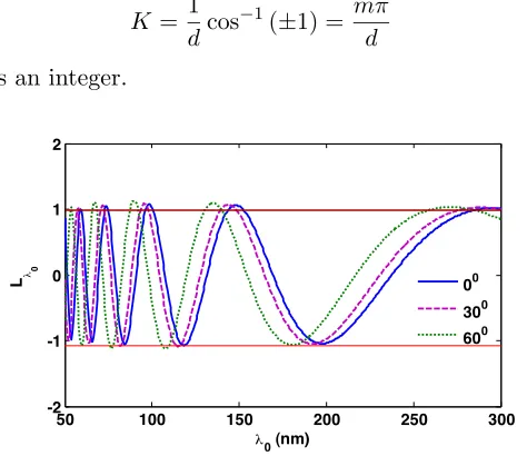
Figure 2. Variation of Lλ0 withλ0 forn1 = 1.5, n2 = 2.2, n3 = 1.5,
d1 = 0.85d, d2 = 0.85×(0.15d), d3 = 0.15×(0.15d) and d= 140 nm
at angles of incidence equal to 0◦, 3 0◦, and 60◦.
2000 2500 3000 3500 4000
-2 -1 0 1 2
L λ
0
λ0 (nm) 00
300
600
Figure 3. Variation ofLλ0 withλ0 for [n1 = 3.6,n2= 1.52,n3 = 3.6,
d1 = 0.85d,d2 = 0.85×(0.15d),d3 = 0.15×(0.15d) and d= 3000 nm
For this proposed filterK satisfies Eq. (7) cosβ1cosβ2cosβ3−
1 2
p2
p1
+p1 p2
sinβ1sinβ2cosβ3 −1
2
p2
p3
+p3 p2
cosβ1sinβ2sinβ3−
1 2
p1
p3
+p3 p1
sinβ1cosβ2sinβ3
= cos{K(d1+d2+d3)} (15)
Now abbreviating the LHS as Lλ0 Eq. (15) can be written as
Lλ0 = cos (kd) (16)
where the LHS (Lλ0) of Eq. (15) in terms of free space wavelength (λ0)
can be written as
Lλ0=cos
2πn1d1
λ0
1−sin
2θ
A n21
1 2
cos
2πn2d2
λ0
1−sin
2θ
A n22
1 2
cos
2πn3d3
λ0
1−sin
2θA n2 3 1 2 −1 2
n22
1−sin
2θ A n2 2 1 2
n21
1−sin
2θA n2 1 1 2 + n21
1−sin
2θ A n2 1 1 2
n22
1−sin
2θA n2 2 1 2 × sin
2πn1d1
λ0
1−sin
2θA n2 1 1 2 sin
2πn2d2
λ0
1−sin
2θA n2 2 1 2 cos
2πn3d3
λ0
1−sin
2θ
A n23
1 2 −1 2 n2 3
1−sin
2θ A n2 3 1 2 n2 2
1−sin
2θ
A n22
1 2 + n2 2
1−sin
2θ A n2 2 1 2 n2 3
1−sin
2θ
A n23
1 2 × cos
2πn1d1
λ0
1−sin
2θ
A n21
1 2
sin
2πn2d2
λ0
1−sin
2θ
A n22
1 2
400 450 500 550 600 650 700 750 800 -2 -1 0 1 2 L λ 0
λ0 (nm)
00
300
600
Figure 4. Variation ofLλ0 withλ0 for [n1 = 2.6,n2= 1.52,n3 = 2.6,
d1 = 0.85d, d2 = 0.85×(0.15d), d3 = 0.15×(0.15d) and d= 600 nm
at angles of incidence equal to 0◦, 3 0◦, and 60◦.
sin
2πn3d3
λ0
1−sin
2θ
A n23
1 2 −1 2
n21
1− sin
2θ A n2 1 1 2 n2 3
1− sin
2θ
A n23
1 2
+ n23
1−sin
2θ A n2 3 1 2 n2 1
1−sin
2θ
A n21
1 2 × sin
2πn1d1
λ0
1− sin
2θ
A n21
1
2
cos
2πn2d2
λ0
1−sin
2θ
A n22
1
2
sin
2πn3d3
λ0
1−sin
2θA
n2 3
1
2
This dispersion equation will determine the allowed and forbidden ranges of wavelengths.
3. RESULT AND DISCUSSION
Table 2. Photonic bandgap for [n1 = 3.6, n2 = 1.52, n3 = 3.6,
d1 = 0.85d,d2 = 0.85×(0.15d), d3 = 0.15×(0.15d), d= 3000 nm].
Angle of Incidence (θA)
Infrared Region Allowed
Bands
Allowed Ranges (nm)
Band Width (nm)
0
1 2048–2160 112
2 2288–2428 140
3 2588–2768 180
4 2972–3228 256
5 3492–3872 380
π 6
1 2028–2132 104
2 2264–2396 132
3 2560–2736 176
4 2944–3188 244
5 3456–3824 368
π 3
1 2000–2076 76
2 2216–2332 116
3 2504–2664 160
4 2880–3108 228
5 3384–3728 344
0.85d,d2 = 0.85×(0.15d) andd3= 0.15×(0.15d) whered= 140 nm, is
the period of the structure. Investigations are also repeated for infrared and visible regions of electromagnetic spectrum by changing the period of the structure as 3000 nm and 600 nm respectively. Keepingn1 = 3.6,
n2 = 1.52 and n3 = 3.6 for infrared region and n1 = 2.6, n2 = 1.52
and n3= 2.6 for visible region.
Using these values in Eq. (15)Lλ0 is plotted against the free space
the width of the allowed photonic bands increases as the wavelength increases. The width of the allowed photonic bands is maximum at 0◦ i.e., normal incidence and as the angle of incidence increases the width decreases, for fixed values ofn1,n2,n3,d1,d2, andd3 as shown in the
Tables 1, 2 and 3respectively. Actually these allowed bands give the different ranges of wavelengths that can be transmitted through the filter structure. The ranges of transmission depend on the values of controlling parameters n1, n2, n3, d1, d2, and d3. Thus by choosing
suitable values of these parameters one can get the desired range of transmission (or reflection).
Table 3. Photonic bandgap for [n1 = 2.6, n2 = 1.52, n3 = 2.6,
d1 = 0.85d,d2 = 0.85×(0.15d), d3 = 0.15×(0.15d), d= 600 nm].
Angle of Incidence (θA)
Visible Region Allowed
Bands
Allowed Ranges (nm)
Band Width (nm)
0
1 400–412 12
2 432–479.2 47.2
3 507.2–573.6 66.4
4 612–716 104
5 768.8–800 31.2
π 6
1 400–402.4 2.4
2 424–468 44
3 496.8–560.8 64
4 600–700 100
5 754.4–800 45.6
π 3
1 406.4–445.6 39.2 2 476.8–534.4 57.6
3 576–667.2 91.2
4 724–800 76
-4. CONCLUSION
In this work we have suggested the matrix formulation method for finding out dispersion relation for 1D ternary PBG structure. Using this dispersion relation we have suggested a design of an optical filter which can work for all the ranges of electromagnetic spectrum by choosing the suitable values of controlling parameters. This study can be used to develop more efficient and accurate photonic band gap material based tunable optical filter. The proposed optical filter made of 1-D ternary PBG material filters more number of allowed bands as compared to a filter made of 1-D binary PBG material and with better control in the wavelength of allowed bands to be filtered.
ACKNOWLEDGMENT
The author would like to thank Dr. Ashok K. Chauhan, Founder President, Amity University, (Noida) India for his constant interest and encouragement. Thanks are also due to Prof. U. Malaviya for her valuable suggestions and insights and Prof. S. N. Shukla for discussions during the preparation of the manuscript.
REFERENCES
1. Yablonovitch, E., “Inhibited spontaneous emission in solid-state physics and electronics,” Phys. Rev. Lett., Vol. 58, 2059–2062, 1987.
2. John, S., “Strong localization of photons in certain disordered dielectric superlattices,” Phys. Rev. Lett., Vol. 58, 2486–2489, 1987.
3. Makhan, M. and S. K. Ramchurn, “Polarization-independent omnidirectional defect modes in Bragg gaps of one-dimensional photonic crystals,”J. Opt. Soc. Am. B, Vol. 24, 3040–3047, 2007. 4. Joannopoulos, J. D., P. R. Villeneuve, and S. Fan, “Photonic crystals: Putting a new twist on light,” Nature, Vol. 386, 143– 149, 1997.
5. Zheng, Q. R., Y. Q. Fu, and N. C. Yuan, “Characteristics of planar PBG structures with a cover layer,” Journal of Electromagnetic Waves andApplications, Vol. 20, No. 11, 1439–1453, 2006. 6. Fink, Y., J. N. Winn, S. Fan, C. Chen, and J. Michel, “A dielectric
7. Rojas, J. A. M., J. Alpuente, J. Pi¨Eœneiro, and R. Sanchez, “Rig-orous full vectorial analysis of electromagnetic wave propagation in 1D,”Progress In Electromagnetics Research, PIER 63, 89–105, 2006.
8. Chigrin, D. N., A. V. Lavrinenko, D. A. Yarotsky, and S. V. Gaponenko, “Observation of total omnidirectional reflection from a one-dimensional dielectric lattice,”Appl. Phys. A, Vol. 68, 25–28, 1999.
9. Sakoda, K., Optical Properties of Photonic Crystals, Springer-Verlag, Berlin, 2001.
10. Han, P. and H. Wang, “Extension of omnidirectional reflection range in one-dimensional photonic crystal with a staggered structure,” J. Opt. Soc. Am. B, Vol. 20, No. 9, 1996–2001, 2003. 11. Ozbay, E., M. Bayindir, I. Bulu, and E. Cubukcu, “Investigation
of localized coupled-cavity modes in two-dimensional photonic bandgap structures,” IEEE J. of Quantum Electronics, Vol. 38, 837–843, 2002.
12. Boroditsky, M., R. Vrijen, T. F. Krauss, R. Coccioli, R. Bhat, and E. Yablonovitch, “Spontaneous emission extraction and Purcell enhancement from thin-film 2-D photonic crystals,”J. Lightwave Technol., Vol. 17, 2096–2112, 1999.
13. Painter, O., R. K. Lee, A. Scherer, A. Yariv, J. D. O’Brien, P. D. Dapkus, and I. Kim, “Two dimensional photonic bandgap defect mode laser,” Science, Vol. 284, 1819–1821, 1999.
14. Mekis, A., M. Meier, A. Dodabalapur, R. E. Slusher, and J. D. Joannopoulos, “Lasing mechanism in two-dimensional photonic crystal lasers,” Appl. Phys. A: Materials Science and Processing, Vol. 69, 111–114, 1999.
15. Noda, S., M. Yokoyama, M. Imada, A. Chutinan, and M. Mochizuki, “Polarization mode control of two-dimensional photonic crystal laser by unit cell structure design,” Science, Vol. 293, 1123–1125, 2001.
16. Mekis, A., J. C. Chen, I. Kurland, S. Fan, P. R. Villeneuve, and J. D. Joannopoulos, “High transmission through sharp bends in photonic crystal waveguides,” Phys. Rev. Lett., Vol. 77, 3787– 3790, 1996.
17. Sondergaard, T. and K. H. Dridi, “Energy flow in photonic crystal waveguides,”Phys. Rev. B, Vol. 61, 15688–15696, 2000.
19. Brown, E. R., C. D. Parker, and E. Yablonovitch, “Radiation properties of a planar antenna on a photonic-crystal substrate,”
J. Opt. Soc. Amer. B, Vol. 10, 404–407, 1993.
20. Kosaka, H., T. Kawashima, A. Tomita, M. Notomi, T. Tamamura, T. Sato, and S. Kawakamib, “Photonic crystals for micro lightwave circuits using wavelength dependent angular beam steering,”
Appl. Phys. Lett., Vol. 74, 1370–1372, 1999.
21. Villeneuve, P. R., D. S. Abrams, S. Fan, and J. D. Joannopoulos, “Single-mode waveguide microcavity for fast optical switching,”
Opt. Lett., Vol. 21, 2017–2019, 1996.
22. Zandi, O., Z. Atlasbaf, and K. Forooraghi, “Flat multilayer dielectric reflector antennas,” Progress In Electromagnetics Research, PIER 72, 1–19, 2007.
23. Aissaoui, M., J. Zaghdoudi, M. Kanzari, and B. Rezig, “Optical properties of the quasi-periodic one-dimensional generalized multilayer Fibonacci structures,” Progress In Electromagnetics Research, PIER 59, 69–83, 2006.
24. Maka, T., D. N. Chigrin, S. G. Romanov, and C. M. S. Torres, “Three dimensional photonic crystals in the visible regime,”
Progress In Electromagnetics Research, PIER 41, 307–335, 2003. 25. Wu, C.-J., “Transmission and reflection in a periodic
supercon-ductor/dielectric film multilayer structure,” Journal of Electro-magnetic Waves andApplications, Vol. 19, 1991–1996, 2005. 26. Delano, E. and R. J. Pegis, Progress in Optics, E. Wolf (ed.),
Chap. 7, Vol. 69, North-Holland, Amsterdam, 1969.
27. Banerjee, A., S. K. Awasthi, U. Malaviya, and S. P. Ojha, “Design of a nano-layered tunable optical filter,” Journal of Modern Optics, Vol. 53, No. 12, 1739–1752, 2006.
28. Brooks, D. and S. Ruschin, “Integrated electrooptic multielec-trode tunable filter,” J. Lightwave Technol., Vol. 13, 1508–1513, 1995.
29. Wooten, E. L., R. L. Stone, E. W. Miles, and E. M. Bradely, “Rapidly tunable narrowband wavelength filter using LiNbO3,”
J. Lightwave Technol., Vol. 14, 2530–2536, 1996.
30. Oda, K., N. Yakato, T. Kominato, and H. Toba, “A 16-channel frequency selection switch for optical FDM distribution systems,”
IEEE J. Sel. Areas Commun., Vol. 8, 1132–1140, 1990.
31. Stone, J. and L. W. Stulz, “High-performance fibre Fabry-Perot filters,”Electron. Lett., Vol. 27, 2239–2240, 1991.
1980.
33. Zirngibl, M., C. H. Joyner, and B. Glance, “Digitally tunable channel-dropping filter/equalizer based on waveguide grating router and optical amplifier integration,” IEEE Photonics Technol. Lett., Vol. 6, 513–515, 1994.
34. Ishida, O., H. Takahashi, and Y. Inoue, “Digitally tunable optical filters using arrayed-waveguide grating (AWG) multiplexers and optical switches,”J. Light Wave Technol., Vol. 15, 321–327, 1997. 35. Sneh, A. and K. M. Johnson, “High-speed tunable liquid crystal filter for WDM networks,” J. Lightwave Technol., Vol. 14, 1067– 1080, 1996.
36. Chen, P. L., K. C. Lin, W. C. Chuang, Y. C. Tzeng, K. Y. Lee, and W. Y. Lee, “Analysis of a liquid crystal Fabry-Perot etalon filter: A novel model,” IEEE Photonics Technol. Lett., Vol. 9, 467–469, 1997.
37. Fujii, Y., “High-isolation polarization-independent optical circu-lator coupled with single-mode fibers,” J. Lightwave Technol., Vol. 9, 456–460, 1991.
38. Smith, D. A., J. E. Baran, J. J. Johnson, and K. W. Cheung, “Integrated-optic acoustically tunable filters for WDM networks,”
IEEE J. Sel. Areas Commun., Vol. 8, 1151–1159, 1990.
39. Zhao, L. P., X. Zhai, B. Wu, T. Su, W. Xue, and C.-H. Liang, “Novel design of dual-mode bandpass filter using rectangle structure,”Progress In Electromagnetics Research B, Vol. 3, 131– 141, 2008.
40. Jopson, R. M., J. Jtone, and L. W. Stulz, “Nonreciprocal transmission in a fiber Fabry-Perot resonator containing a magneto optic material,” Photonics Tech. Lett., Vol. 2, 702–704, 1990.
41. Morishita, K., “Optical fiber devices using dispersive materials,”
IEEE J. Lightwave Technol., Vol. 7, 198–201, 1989.
42. Reid, D. C. J., C. M. Rogdale, I. Robbins, D. J. Robbins, J. Buus, and W. J. Stewart, “Phase-shifted Moire grating fibre resonators,”
Electron. Lett., Vol. 26, 10–12, 1990.
43. Ojha, S. P., P. K. Chaudhary, P. Khastgir, and O. N. Singh, “Operating characteristics of an optical filter with a linearly periodic refractive index pattern in the filter material,” Jpn. J. Appl. Phys., Vol. 31, 281–285, 1992.
45. D’Orazio, A., M. de Sario, V. Petruzzelli, and F. Prudenzano, “Photonic band gap filter for wavelength division multiplexer,”
Opt. Exp., Vol. 11, No. 3, 230–239, 2003.
46. DelVillar, I., I. R. Matias, F. J. Arregui, and R. O. Claus, “Analysis of one-dimensional photonic bandgap structures with a liquid crystal defect toward development of fiber-optic tunable wavelength filters,” Opt. Exp., Vol. 11, No. 5, 430–436, 2003. 47. Awasthi, S. K., U. Malaviya, and S. P. Ojha, “Enhancement of
omnidirectional total reflection wavelength range by using one-dimensional ternary photonic bandgap material,” J. Opt. Soc. Am. B, Vol. 23, 2566–2571, 2006.
48. Born, M. and E. Wolf, “Basic properties of the electromagnetic field,” Principles of Optics, 1–70, Cambridge University Press, U.K., 1980.
49. Orfanidis, S. J., “Multilayer film applications,” Electromagnetic Waves andAntennas, 193–194,

![Table 1.Photonic bandgap for [n1 = 1.5, n2 = 2.2, n3 = 1.5,d1 = 0.85d, d2 = 0.85 × (0.15d), d3 = 0.15 × (0.15d), d = 140 nm].](https://thumb-us.123doks.com/thumbv2/123dok_us/7731636.1265824/6.612.109.423.131.584/table-photonic-bandgap-for-n-n-n-nm.webp)
![Table 2.Photonic bandgap for [dn1 = 3.6, n2 = 1.52, n3 = 3.6,1 = 0.85d, d2 = 0.85 × (0.15d), d3 = 0.15 × (0.15d), d = 3000 nm].](https://thumb-us.123doks.com/thumbv2/123dok_us/7731636.1265824/10.612.103.426.135.398/table-photonic-bandgap-for-dn-n-n-nm.webp)
![Table 3.Photonic bandgap for [n1 = 2.6, n2 = 1.52, n3 = 2.6,d1 = 0.85d, d2 = 0.85 × (0.15d), d3 = 0.15 × (0.15d), d = 600 nm].](https://thumb-us.123doks.com/thumbv2/123dok_us/7731636.1265824/11.612.107.418.267.531/table-photonic-bandgap-for-n-n-n-nm.webp)
