Lehigh University
Lehigh Preserve
Theses and Dissertations
2017
Microstructural Evolution and Mechanical
Property Development of Selective Laser Melted
Copper Alloys
Anthony Patrick Ventura
Lehigh University
Follow this and additional works at:http://preserve.lehigh.edu/etd Part of theMaterials Science and Engineering Commons
This Dissertation is brought to you for free and open access by Lehigh Preserve. It has been accepted for inclusion in Theses and Dissertations by an authorized administrator of Lehigh Preserve. For more information, please [email protected].
Recommended Citation
Ventura, Anthony Patrick, "Microstructural Evolution and Mechanical Property Development of Selective Laser Melted Copper Alloys" (2017).Theses and Dissertations. 2857.
Microstructural Evolution and Mechanical Property
Development of Selective Laser Melted Copper Alloys
by
Anthony Patrick Ventura
Presented to the Graduate and Research Committee of Lehigh University
in Candidacy for the Degree of Doctor of Philosophy
in
Materials Science and Engineering
Lehigh University May 2017
ii
© Copyright Anthony P. Ventura May 2017
iii
Approved and recommended for acceptance as a dissertation in partial fulfillment of the requirements for the degree of Doctor of Philosophy.
____________________ Date
__________________________ Prof. Wojciech Misiolek, Advisor
____________________ Accepted Date
__________________________ Prof. Wojciech Misiolek, Chair
__________________________ Prof. Masashi Watanabe
__________________________ Prof. Richard Vinci
__________________________ Dr. Gregory Pawlikowski
__________________________ Dr. Ahmad Chamanfar
iv
ACKNOWLEDGEMENTS
I would like to thank my advisor, Dr. Wojciech Misiolek. His insistence for graduate students to take charge of their own research allows them to find their own path to success and develop into confident engineers. He has always encouraged me to take on just a bit more responsibility than I was aware I could handle, and the trust he has placed in me has always been the catalyst for my progress. It has been a pleasure to study metallurgy under your guidance, you have been a great mentor in my life.
Two organizations have enabled me to conduct this research. I have been financially supported by the Loewy Family Foundation for many years. Mrs. Linz and the foundation have shaped my career, and their stewardship of research and education has left a lasting impression on me. TE Connectivity has funded a significant portion of this research. Greg Pawlikowski and Martin Bayes have always been supportive of my research efforts and this work would not have been possible without them.
To all members of the Materials Science & Engineering Department family and the Loewy Institute, thank you for your support. The fellowship of graduate students, past and present, that I have learned alongside; you have all been wonderful colleagues and friends. Special thanks go to Mike Rex, Arlan Benscoter, Lisa Arechiga, and Katrina Kraft for tolerating all of us in our time at Lehigh.
v
To my friends, Marc, Andrew, Amelia, Matt, Rosey and many others: thank you for helping bring balance to my life and all the fun times we have together. Mario Epler, thank you for your friendship and guidance at many LVASM meetings.
I am grateful to all my professors at Lehigh University, and especially those that are serving on my doctoral committee: Dr. Masashi Watanabe and Dr. Richard Vinci. They have been overwhelmingly helpful and positive in every regard. I could not possibly ask for better guidance in my academic life.
Very special thanks go to Janie Carlin and Rus Van Westervelt. Janie’s warm smile and welcome conversation made every day in Whitaker brighter; I can’t imagine my time at Lehigh without her. Rus Van Westervelt, thank you for encouraging me to live deliberately, and learn all that life has to teach. You have both had a positive impact on every aspect of my life.
Without the love and support of my family, I would not have made it here today. To my mom, dad, and older brother: thank you for raising me and always being there for me, even in times when I was miserable company. You have helped me every step of the way and I love you. To the Couillards, I could not have imagined a more loving family to become a part of.
Finally, I must thank my wonderful wife, Beth. She never fails to be my better half. I love you, and our life together will always be the most important thing to me.
vi
For my grandfather
Hector C. Ventura
vii
TABLE OF CONTENTS
ACKNOWLEDGEMENTS ... iv
TABLE OF CONTENTS ... vii
LIST OF TABLES ... x LIST OF FIGURES ... xi ABSTRACT ... 1 CHAPTER 1 INTRODUCTION ... 3 1.1 Additive Manufacturing ... 3 1.2 Metal AM Technologies ... 6
1.3 Motivation and Research Objective ... 10
1.4 Dissertation Structure ... 12
CHAPTER 2 BACKGROUND ... 13
2.1 Description of the Selective Laser Melting Process ... 13
2.2 Characteristics of Metal Alloys Fabricated via SLM ... 17
2.3 The Physical Metallurgy of Copper Alloys ... 26
2.3.1 Overview of Copper Alloys ... 26
2.3.2 Introduction to the Conductivity of Copper Alloys ... 28
2.3.3 Principle Strengthening Mechanisms of Copper Alloys ... 29
2.3.3.1 Work (Strain) Hardening ... 29
2.3.3.2 Hall-Petch Strengthening (Grain Boundary Strengthening) ... 33
2.3.3.3 Solid Solution Strengthening... 36
2.3.3.4 Precipitation Hardening (Strengthening) ... 41
2.3.3.5 Dispersion Strengthening ... 47
2.3.4 The Cu-Sn System ... 49
2.3.5 The Cu-Ni-Si System ... 53
CHAPTER 3 MECHANICAL PROPERTIES AND MICROSTRUCTURAL CHARACTERIZATION OF Cu-4.3%Sn FABRICATED BY SELECTIVE LASER MELTING ... 64
3.1 Abstract ... 64
viii
3.3 Experimental Methods ... 67
3.4 Results... 70
3.5 Discussion ... 77
3.5.1 Grain Morphology ... 77
3.5.2 Effect of Geometry on Tensile Properties ... 79
3.5.3 Effect of Heat Treatment on Tensile Properties ... 82
3.5.4 High Magnification STEM and EDS ... 86
3.6 Conclusions ... 93
3.7 Acknowledgements ... 94
CHAPTER 4 THE EFFECT OF AGING ON THE MICROSTRUCTURE OF SELECTIVE LASER MELTED Cu-Ni-Si ... 96
4.1 Abstract ... 96
4.2 Introduction ... 97
4.3 Experimental Methods ... 99
4.4 Results... 103
4.5 Discussion ... 111
4.5.1 As-Printed Microstructural Features ... 111
4.5.2 Aging and Precipitation Contributions to Strengthening ... 117
4.5.3 Other Contributions to Mechanical Property Development ... 125
4.6 Conclusions ... 131 4.7 Acknowledgements ... 132 CHAPTER 5 SUMMARY ... 133 5.1 Significance of Findings ... 133 5.2 Future Work ... 134 5.2.1 Fabrication Parameters ... 134
5.2.2 Post-Processing and Other Mechanical Property Metrics ... 135
5.2.3 Copper Alloy Development For SLM ... 137
REFERENCES ... 139
APPENDIX A EXPANDED METHODS ... 147
ix
A.2 SLM Process Parameters ... 148
A.3 Heat Treatment ... 149
A.4 Tensile Testing ... 155
A.5 Metallographic Preparation ... 158
A.6 Microhardness ... 165
A.7 Standard Operating Procedure for Phase ID by XRD ... 166
A.8 Electron Backscatter Diffraction ... 169
A.9 Focused Ion Beam Milling and TEM Sample Preparation ... 171
A.10 Transmission Electron Microscopy... 174
x
LIST OF TABLES
Table 1. UNS C70250 alloy composition specifications.[67]... 53 Table 2. Physical Properties of SLM Cu-4.3%Sn in the As-Printed and
Post-Process Heat Treated Conditions ... 73 Table 3. C70250 powder composition from ECKA Granules specifications. 100
xi
LIST OF FIGURES
Figure 1. Schematic diagram of the SLM process.[19] ... 14 Figure 2. Effective absorptance of a deep powder bed vs dense material
absorptance for various pure metals. Symbols are experimental data and lines are models.[20] ... 16 Figure 3. Change in solidification substructure moving away from the weld line in SLM AlSi10Mg.The build direction is vertical. [24] ... 20 Figure 4. Variation in solidification substructure under different G and R
conditions.[33] ... 21 Figure 5. Epitaxial growth observed in the weld pools of SLM AlSi10Mg.[24] 23 Figure 6. Conductivity vs. ultimate tensile strength for various annealed copper
alloys. [16] ... 28 Figure 7. Work hardening rate (Θ) versus stress (σ) for different strain rates (a and b) with the Voce parameters specified on the axes.[47] ... 32 Figure 8. Approximate effect of solute content on the critical resolved shear
stress at room temperature.[16] ... 38 Figure 9. The effect of small additions of solute atoms on the resistivity of
copper.[58] ... 40 Figure 10. Schematic diagram of the major strengthening mechanisms active
during a precipitation hardening aging heat treatment.[45] ... 43 Figure 11. Copper-Tin equilibrium phase diagram. [16] ... 52 Figure 12. Dark-field micrograph of a CuNiSi alloy aged at 450°C for 750
hours with the beam direction parallel to the <001> of the copper matrix using the (020)ppt diffraction spot for imaging.[68] ... 55
Figure 13. (a) Simulations of the 6 δ-Ni2Si diffraction patterns that are present
when viewing along the <111>Cu (b) the copper and δ-Ni2Si
patterns superimposed and (c) secondary diffraction effects added to (b) next to (d) an experimental pattern.[70] ... 57 Figure 14. Variation in precipitate thickness (▪) and diameter (▫) during aging at
450°C for CuNiSi.[68] ... 58 Figure 15. Schematic free energy curve at sub-critical aging temperatures for
CuNiSi alloys proposed by Zhao et al. [73] ... 61 Figure 16. Prototypical uniaxial tensile test results of SLM Cu-4.3%Sn in the
as-printed condition as well as post-process heat treated at 873 K (600 °C) and 1173 K (900 °C). ... 71
xii
Figure 17. Light optical micrograph of the build direction of as-printed Cu-4.3%Sn etched in Klemm’s I reagent. ... 74 Figure 18. IPF Maps of SLM Cu-4.3%Sn in the (a) as-printed condition, and
after heat treatment at (b) 873 K (600 °C) and (c) 1173 K (900 °C). ... 75 Figure 19. ABF STEM microstructural comparison between SLM Cu4.3%Sn in
the (a) as-printed condition as well as printed and heat treated at (b) 873 K (600 °C) and (c) 1173 K (900 °C). ... 76 Figure 20. Inverse pole figures taken from the transverse direction (parallel to
the build direction) of SLM Cu-4.3%Sn in the (a) as-printed condition as well as heat treatment at (b) 873 K (600 °C) and (c) 1173 K (900 °C). ... 79 Figure 21. Prototypical uniaxial tensile test results of SLM Cu-4.3%Sn in the
as-printed condition 3mm thick, 1mm thick and a sample that was machined from a rectangular prism to 3mm thick. ... 80 Figure 22. Differential interference contrast light optical micrograph of the build
direction of SLM Cu-4.3%Sn heat treated at 873 K (600 °C) etched in Klemm’s I reagent. ... 85 Figure 23. ABF STEM image along the build direction of as-printed SLM
Cu-4.3%Sn showing an individual weld line (dashed line) and
solidification sub-structure... 87 Figure 24. BF- STEM and accompanying XEDS intensity maps of typical small particles observed in the intercellular regions of the as-printed Cu-4.3%Sn. ... 88 Figure 25. XRD pattern obtained from as printed SLM Cu-4.3%Sn. ... 89 Figure 26. ABF-STEM image of oxide particles (dark spots) observed in SLM
Cu-4.3%Sn heat treated at 873 K (600 °C). ... 91 Figure 27. BF-STEM image of oxide particles observed in SLM Cu-4.3%Sn
heat treated at 1173 K (900 °C). ... 92 Figure 28. Physical property evolution of SLM C70250 during aging at 723 K
(450 °C) from the as-printed condition. ... 105 Figure 29. Polarized light optical micrographs of as-printed SLM C70250 in the
(a) build direction and (b) transverse direction. ... 106 Figure 30. Bright-field TEM micrograph of dislocations in the solidification
substructure at the melt pool boundary in as-printed SLM C70250. ... 107 Figure 31. XRD patterns of SLM C70250 at various stages of aging. ... 108
xiii
Figure 32. (a) Dark-field TEM micrograph of the δ-Ni2Si strengthening
precipitates in the peak age condition and (b) the corresponding SAD pattern of the [111]Cu matrix projection. ... 110
Figure 33. (a) Dark-field TEM micrograph of the δ-Ni2Si strengthening
precipitates in the over age condition and (b) the corresponding SAD pattern of the [111]Cu matrix projection. ... 110
Figure 34. Bright-field LOM micrograph of as-printed SLM C70250 showing the change in solidification substructure scale throughout the weld pools. Dashed lines mark the fusion line of two melt pools. ... 114 Figure 35. Bright-field STEM and XEDS intensity maps (normalized to the Cu
intensity) of the solidification substructure at the weld line in as-printed SLM C70250. ... 115 Figure 36. Microhardness and electrical conductivity comparison between
SLM C70250 aged directly after printing (P+A) and samples that had an intermediate homogenization/solution heat treatment
(P+ST+A). ... 119 Figure 37. (a) Secondary electron micrograph of a DP zone in over aged SLM
C70250 (aged for 128 hours). (b) Bright-field TEM micrograph of a precipitate in the DP zone, (c) accompanying SAD pattern along the [110]Cu || [010]δ and (d) the corresponding simulated diffraction
pattern. ... 121 Figure 38. Work hardening rate versus the normalized flow stress for SLM
C70250 at various stages of aging. ... 128 Figure 39. (a) LOM observation and (b) EBSD analysis of deformation
twinning observed in a peak aged SLM C70250 sample deformed in a uniaxial tensile test to failure. The black lines in (b) outline FCC twin boundaries. ... 129 Figure 40. Density vs linear laser energy curve at various beam spot sizes.
This data was utilized to select the ideal processing parameters for samples used in this study. ... 149 Figure 41. Temperature vs time plot showing the maximum ramp rate of the
tube furnace used in this investigation during cross flow of argon gas. ... 152 Figure 42. Oxygen incorporation near the surface of copper samples heat
treated at 900°C in a tube furnace with an additional leak from thermocouple wire insertion. ... 154 Figure 43. Micrograph of a copper sample heat treated in a furnace without a
thermocouple wire inserted, no significant oxide formation is
xiv
Figure 44. The two types of speckle patterns used for DIC strain mapping for (top) as-printed samples and (bottom) machined samples. ... 157 Figure 45. Comparison of LOM contrast after etching with Klemm’s I for 2
minutes 15 seconds in (top) bright-field and (bottom) cross-polarized light. Alloy C70250, build direction, as-printed condition. ... 163 Figure 46. LOM micrograph of contrast after etching with ferric nitrate solution. Alloy C70250, peak age, strained to failure to show twinning. .... 164 Figure 47. Comparison of microhardness measurements taken with different
indentation loads. Alloy C70250, solution treated and aged. ... 166 Figure 48. IPF map obtained from EBSD showing scratches and drifting.
Image quality is overlaid in greyscale. Alloy C70250, as-printed. 170 Figure 49. Examples of FIB damage observed during Ga ion milling of copper. Damaged regions were exposed to (a) 30 keV 50 pA Ga ions and (b) 5keV 100 pA Ga ions.[105] ... 172 Figure 50. Example TEM micrograph showing FIB damage observed in this
1
ABSTRACT
Selective Laser Melting (SLM) is an additive manufacturing technology that utilizes a high-power laser to melt metal powder and form a part layer-by-layer. Over the last 25 years, the technology has progressed from prototyping polymer parts to full scale production of metal component. SLM offers several advantages over traditional manufacturing techniques; however, the current alloy systems that are researched and utilized for SLM do not address applications requiring high electrical and thermal conductivity. This work presents a characterization of the microstructural evolution and mechanical property development of two copper alloys fabricated via SLM and post-process heat treated to address this gap in knowledge. Tensile testing, conductivity measurement, and detailed microstructural characterization was carried out on samples in the as-printed and heat treated conditions.
A single phase solid solution strengthened binary alloy, Cu-4.3Sn, was the first alloy studied. Components were selectively laser melted from pre-alloyed Cu-4.3Sn powder and heat treated at 873 K (600 °C) and 1173 K (900 °C) for 1 hour. As-printed samples were around 97 percent dense with a yield strength of 274 MPa, an electrical conductivity of 24.1 %IACS, and an
elongation of 5.6%. Heat treatment resulted in lower yield strength with significant increases in ductility due to recrystallization and a decrease in dislocation density. Tensile sample geometry and surface finish also showed a significant effect on measured yield strength but a negligible change in
2
measured ductility. Microstructural characterization indicated that grains
primarily grow epitaxially with a sub-micron cellular solidification sub-structure. Nanometer scale tin dioxide particles identified via XRD were found
throughout the structure in the tin-rich intercellular regions.
The second alloy studied was a high-performance precipitation hardening Cu-Ni-Si alloy, C70250. Pre-alloyed powder was selectively laser melted to produce components around 98 percent dense with high mechanical strength and electrical conductivity. Aging heat treatments were carried out at 723 K (450 °C) directly on as-printed samples up to 128 hours. A peak yield strength of around 590 MPa could be attained with an electrical conductivity of 34.2 %IACS after 8 hours of aging. Conductivity continues to increase with further aging while the peak strength appears to be less sensitive to aging time exhibiting a broad range of time where near-peak properties exist. Nanometer-scale silicon-rich oxide particles exist throughout the material and persist during aging. Deformation twinning is observed in the peak age condition after tensile testing and several strengthening mechanisms appear to be active to varying degrees throughout aging, which accounts for the broad range of aging time where nearly the peak mechanical properties exist. The findings of this research are integral to understanding SLM copper alloys and serve as a foundation for future development of new copper alloys tailored to the SLM process.
3
CHAPTER 1
INTRODUCTION
1.1 Additive Manufacturing
Additive manufacturing (AM) refers to a group of technologies that build up a shape layer-by-layer from a three-dimensional computer model. Although the origins of the concept were being explored in the 1950s and 1960s, the first widely used AM technology, stereolithography, was developed by Charles Hull in 1984 to produce polymer prototypes and streamline the design
process. Hull described the process as “A system for generating
three-dimensional objects by creating a cross-sectional pattern of the object to be… automatically formed and integrated together to provide a step-wise laminar buildup of the desired object”.[1] The fundamental principles Hull outlines are present in all modern variations of AM technology. Parts are created from computer aided design (CAD) files that have been “sliced” into individual build layers. Each layer is successively fabricated on top of the previous layer until the part is finished.
The concept of building a part layer-by-layer contrasts with traditional subtractive processes such as machining or multi-step forming processes and fundamentally shapes the design methodology of AM. Originally, AM
technologies were primarily used for prototyping and design purposes explicitly (hence the initial nomenclature of “Rapid Prototyping”). As
4
potential paradigm shift in manufacturing where, extrapolated to the extreme, direct digital manufacturing of customized parts on an as-needed basis is standard practice.[2] In their current form, the various AM technologies serve as powerful prototyping and design tools building upon their original intent with a growing set of applications for manufacturing finished parts. The current state-of-the-art AM technologies produce components of high enough quality to be utilized as finished products and research continues to address the need for improvements in AM part quality.
AM has several advantages over traditional manufacturing techniques. Although there are more intricate sets of advantages and disadvantages for each individual technology, there are many benefits that apply generally to AM as compared to traditional manufacturing. One of the most fundamental and unique advantages is the concept that adding complexity to a component (primarily in the form of more intricate geometries) does not pose a significant challenge or increase in resources. CAD is integral to the design process in modern manufacturing. In AM, the move from CAD to fabrication is essentially seamless. Therefore, a great deal of freedom is introduced to the design process because the capabilities of traditional manufacturing techniques no longer require consideration (i.e. features that are difficult to produce or add prohibitive cost in traditional manufacturing can be included where they are the optimum solution). This results in the ability to create customized components, easily change designs on a short time scale with no additional cost, and
5
streamline the overall design process.[2] “Free complexity” is also the root cause of the low material waste and reduction in number of processing steps required to make a finished component in AM. In nearly all AM technologies, excess material that is not directly utilized to fabricate the component can be recycled. As a result, AM does not waste a significant amount of raw material and falls under the categorization of a near-net shape process.[3] All features of the finished component are formed during a single-step process which eliminates processing steps. The more complex a part is, the more significant these advantages can become. As a result, AM is a particularly attractive option for biomedical and aerospace industries where increased complexity can have significant effects on performance.[4]
AM struggles to compete with traditional manufacturing techniques due to several key disadvantages. One issue is the cost and low production rate for large quantities of components. Although the batch nature of AM
technologies allows for some degree of flexibility, the process generally has poor economies of scale and does not become significantly more cost
effective for large production runs of the same component. Additionally, there is a fixed amount of set up before each production batch, so producing more parts does not result in increased production efficiency.[5] Another significant disadvantage of AM is the low mechanical performance compared to
traditionally manufactured materials. There are often imperfections such as porosity, surface roughness, and contamination which degrade the bulk
6
physical properties of the material.[2] Increasing the reliability and diversity of all types of materials fabricated by AM is one of the current primary research objectives in the field.
1.2 Metal AM Technologies
Polymers were traditionally the materials of choice for AM due to their ease of processing, particularly in the common commercial technology
stereolithography where photopolymerization is the mechanism for fabrication. However, as the field progressed, several technologies were developed that could process metal alloys. The ability to process metals drastically expanded the attainable properties and applications of AM.[2] The most common AM technologies that are applicable to metal systems can be divided broadly into binder jetting, direct energy deposition (beam deposition) and powder bed fusion. Note that although other technologies exist for metal AM, only the most prolific methods are briefly introduced here.
Binder jetting is closely related conceptually to the established powder metallurgy process of metal injection molding that employs a polymer binder and metal powder to eventually produce a metal part.[6] A print head sprays a polymer binder into a powder bed in a layer-by-layer fashion. The part that emerges is known as a “green body” as the metal powder is primarily held together by the binder phase and has not been fully densified. Extensive post processing is required to remove the binding phase and produce high density metal component. The post processing consists of either a traditional furnace
7
sintering (sometimes hot isostatic pressing is employed where high pressure aids in consolidation) or infiltration with a lower melting temperature alloy. Sintering involves a substantial amount of shrinkage and distortion that must be designed for which in practice is quite difficult given the low initial density of the green body. In the case of infiltration, the component is typically composed of 60% of the build powder and 35% of the infiltrant (the remaining 5% is indicative of typically porosity levels) so the attainable properties are limited substantially by the infiltrant (the most common implementation of this technique is bronze used to infiltrate stainless steel parts). The extensive amount of post-processing distinguishes binder jetting as an indirect metal AM technology and the potential for novel implementations limited compared to direct energy deposition and powder bed fusion which can directly produce high density metal components.[2,7]
Direct energy deposition (DED) is in many ways similar to established welding technology but is distinguishable by CAD input data and machines designed to create complex 3D shapes. In DED a focused beam of energy, for example an arc, electron beam, or laser, is used to melt feed material that is directly laid onto the fabrication bed/part. The most common feed material is metal powder because it allows for greater geometrical control, however wire fed systems also exist with higher deposition rates at the expense of feature resolution. Fully dense metal components can be produced via this technique, and functionally graded material composition is possible. However, the feature
8
resolution and surface finish of DED processes is poor and in order to achieve better accuracies the deposition rate must be decreased to low levels.
Additionally the geometrical complexity in DED is limited due to the lack of a support structure which limits the types of fully functional parts the technology can produce. Nevertheless, the precise composition control and ease of implementation is a substantial benefit of DED technologies. The processes see limited use for fully finished components, but they are well established for use in coatings, repair, and feature addition when combined with CNC
machining.[2,7]
Powder bed fusion (PBF) technologies are currently the AM technology of choice for fabrication of high density, geometrically complex, and fully functional metal components. The process is schematically similar to binder jetting in that the raw material is supplied in the form of a bed of powder metal. The key difference is the implementation of a high-energy beam to fully melt the powder bed rather than a jet of polymer binder that requires
post-fabrication densification. The resulting parts are fully functional, high density components that can be implemented directly after fabrication. There are two primary forms of PBF for metals; electron beam melting (EBM) that, as the name implies, utilizes an electron beam to melt the powder and Selective Laser Melting (SLM) which utilizes a laser as the energy source. An
9
here, but a detailed description of the SLM process, the primary focus of this work, is presented in Chapter 2.
The two main types of PBF in the form of EBM and SLM are very similar, but EBM has several characteristics that are disadvantageous from a commercial standpoint. Electrons used to heat the powder bed must be carried away from the initial focal point, so EBM processing is limited by the conductivity of the build material. The process therefore works almost exclusively on metals, which are good conductors, and there are some processing limitations on relatively low conductivity alloys (e.g. steels). The use of an electron beam also necessitates a vacuum to operate which increases machine cost and maintenance. The recyclability of powder metal feed stock in EBM can also be an issue. The powder bed is maintained at a higher temperature during fabrication compared to SLM due to the nature of heating with an electron beam. The beam is typically used to broadly heat the powder bed and minimize the necessity for high electron beam density which causes a highly localized negative charge. The negative charge can repel the incoming electron beam or cause neighboring powder particles to repel each other; both of these phenomena cause significant build defects and can cause a build to fail. However, the high powder bed temperature typically leads to some degree of solid state sintering in the lower powder layers during
fabrication. A significant amount of agglomeration can then occur which affects the flow characteristics of the powder and limits the number of runs a
10
particular batch of powder may be used. This also results in a poor surface finish and feature resolution compared to SLM. Although EBM is still employed in industry and has potential for further development, the disadvantages when compared to SLM have generally resulted in the most successful metal PBF companies commercializing the SLM approach.[2] SLM has seen a significant number of developments in recent years including higher power lasers and more sophisticated process modelling. However, there are still shortcomings that must be addressed to improve the process and meet emerging industrial demands. The limited number of alloy systems employed in SLM in particular limits growth of the technology into new markets. Developing new material systems with desirable physical properties is one of the primary goals of modern SLM research.[4]
1.3 Motivation and Research Objective
A significant amount of work exists on SLM of structural alloys with the primary goal of characterizing alloys adapted from traditional manufacturing techniques with high as-printed density as the primary metric of success. Various types of steel, stainless steel, titanium, nickel, and aluminum alloys have been the focus in literature.[5,8-15] Currently, there are no commercially available electrical-grade copper alloys for SLM nor does a significant amount of literature on additively manufactured copper alloys exist. Thus, the
possibility of using SLM for applications requiring high electrical or thermal conductivity is drastically limited. Potential applications for SLM copper alloys
11
include prototyping and full production of electrical connectors, lead frames and metal contacts for integrated circuits, novel thermal dissipation and heat exchanger geometries, as well as self-lubricated bushings.[16]
The objective of this work is to characterize the microstructural
evolution and mechanical property development of copper alloys fabricated via SLM. From a practical standpoint, this research will provide immediate
characterization of two different copper alloys which can be used to create functional components with a wide range of physical properties. This will immediately meet demand for conductive alloys in SLM and allow the
technology to be employed in new applications. Perhaps more importantly, this work will address the gap in literature to understand how the microstructure, properties, and post-processing response of common copper alloys is affected when they are fabricated via SLM. The investigation will include individual analysis of two separate alloys. A simple binary alloy will be characterized to understand fundamental SLM microstructural features and post-processing heat treatment on solid solution strengthened single phase copper alloys. This will to develop a baseline processing window and set of attainable properties. The second alloy is a high-performance precipitation hardened alloy
commonly used in electrical connectors in the wrought form. This alloy will provide important insight into the property development of traditional alloys when they are fabricated via SLM. The results from both alloys will establish an understanding of some of the unique microstructural features SLM
12
introduces into copper alloys and how they interact with the strengthening mechanisms present in common copper alloys.
1.4 Dissertation Structure
The research performed in this investigation is divided into two distinct sections based on the foundation of selective laser melting as the common fabrication technique for two different copper alloys: binary alloy Cu-4.3Sn and alloy C70250. Chapter 2 presents a detailed background on the fundamental concepts of SLM and general copper alloy physical metallurgy that are relevant to both investigations, as well as sections specifically tailored to the particular alloys studied.
The two investigations are presented in Chapters 3 and 4 in the form of manuscripts suitable for individual publication. The first investigation in
Chapter 3 is on the Cu-4.3Sn binary alloy.[17] The second investigation in Chapter 4 is on the precipitation hardened Cu-Ni-Si alloy C70250. Since the investigations are presented as publication-style manuscripts, they appear as full standalone documents with separate abstract, introduction, methods, results, discussion and conclusions sections. The introduction and methods sections are condensed versions of Chapter 2 and Appendix A tailored to each study and as a result, there is some overlap in the topics covered and the references utilized. Chapter 5 serves to summarize the broader implications of the findings, including discussion about the relationship of the findings and their implications with regards to future work on SLM of copper alloys.
13
CHAPTER 2
BACKGROUND
2.1 Description of the Selective Laser Melting Process
Selective Laser Melting (SLM) is a powder bed fusion based additive manufacturing technology that utilizes a high-power laser to melt metal powder. SLM is the nomenclature for modern systems intended to fully melt metal powder during fabrication. These systems were developed from the original selective laser sintering (SLS) machines used for polymers patented in 1990.[18] The technology progressed from exclusively polymer applications to indirect metal processing with a binder. Direct metal components were eventually fabricated with relatively poor properties that utilized low melting temperature metal alloys as liquid phase sintering aids. The state-of-the-art metal SLM currently utilizes full melting of powders for direct metal fabrication. The SLM designation was generally adopted in literature when direct metal fabrication became possible in the machines, and it distinguishes the machines from SLS machines intended only for polymer processing.[2]
Figure 1 shows a schematic diagram of the SLM process. A laser is generated and passes through a micro-mirror device to scan the powder bed per instructions from the build file. An f-θ lens is employed to minimize
distortion and ensure the laser focal plane is flat on the powder bed. The first build layer is completed on top of a build platform, and typically a support structure is fabricated before the actual bulk of the part. After a build layer is
14
completed, the build platform is lowered by a piston around 20-100 µm and powder is spread over the build container for the next layer. Numerous powder spreading techniques are employed by commercial systems. The most typical systems utilize either a feed container or gravity-based dosing system in combination with a powder blade or roller. Figure 1 depicts a feed container and roller setup, but regardless the result is a new layer of powder that will be used to fabricate the next build layer of the component. The process is
repeated until the part is finished. Any powder that was not melted by the laser and integrated into the component is typically vacuumed, sieved, and recycled for future builds. The part is finally removed from the baseplate by machining and any post-processing required is completed. Typical post-processing steps include heat treatment, surface finishing, and secondary machining.
Figure 1. Schematic diagram of the SLM process.[19]
Similar to the function of shielding gas during welding, the build chamber must be an inert atmosphere to avoid incorporation of impurities in
15
the melt pool. The chamber is evacuated and backfilled with nitrogen or argon. Argon is more common as a shielding gas because it can be used in the processing of titanium alloys where nitrogen would react with the molten titanium. During the process, there is an additional cross flow of inert gas to carry away any ablated material or fine particulate matter that has been ejected from the powder bed by the laser. [2]
Modern metal SLM systems utilize Nd:YAG or fiber lasers with a wavelength around 1 µm in contrast to the original CO2 lasers from SLS
development with a larger wavelength (~10 µm). Figure 2 shows the effective absorptance of a powder bed compared to a dense material for various pure metals.[20] The smaller wavelength is better absorbed by metal powders, and there is an added benefit that fiber lasers are more cost effective and require less maintenance than CO2 lasers.[4] Generally, metal alloy absorption of laser
energy is poor, but the powder bed serves to redirect a significant amount of the reflected energy back to other particles and dramatically enhance effective absorptance. Most alloy systems utilized in SLM benefit from smaller
wavelength radiation, but the change for copper systems is quite dramatic. For 10.6 µm wavelength radiation (CO2 laser), pure copper has an absorptance of
around 3% compared to 10% for 1.06 µm wavelength radiation (Nd:YAG laser). Considering a powder bed instead of a dense material (e.g. a copper plate), the effective absorptance of Nd:YAG and fiber laser wavelengths increases to approximately 60% for pure copper powder.[20, 21] Additional
16
changes in the maximum laser power available in commercial machines that provides a much greater effective heat input occurred simultaneously.
Figure 2. Effective absorptance of a deep powder bed vs dense material absorptance for various pure metals. Symbols are experimental data and lines
are models.[20]
There are several processing parameters that can be altered in SLM. The most important parameters with regards to performance of SLM
components fundamentally alter the applied energy density (alternatively, energy input). These parameters control the degree of melting/heating and ultimately determine the microstructure of the finished part. The primary parameters that can be manipulated are the laser power, spot size, scan speed, scan spacing and scan strategy. A large body of research exists on the
17
optimization of these parameters to create functional components.[2,7,9,12] Density generally takes precedence in determining successful build
parameters due to the significant effect of porosity on mechanical properties, regardless of the underlying microstructure. As a result, machine parameters are typically evaluated to produce high density components. However, within the processing window of acceptably high density values, changes in laser parameters can create vastly different microstructures which affect bulk properties.[22–24] These studies highlight the importance of investigating the unique microstructural features present in different alloys fabricated by SLM.
2.2 Characteristics of Metal Alloys Fabricated via SLM
The objective of this research is to characterize copper alloys fabricated via SLM, however the utilization of copper alloys in SLM, and indeed even in most metal AM technologies, is lacking. Pure copper and high copper alloys have seen some use in electron beam melting (EBM) because high
conductivity powders lend themselves well to the EBM process. Although the EBM process is in many ways similar to SLM, it is less flexible in material choice, often has a poorer surface finish compared to SLM, and is less production robust.[4] Still, the microstructures in EBM and SLM components do have some similarities. Fine cellular substructures with segregation of second phase particles from the source powder is observed in EBM copper, but the investigations are generally limited to commercially pure copper with poor mechanical properties.[25, 26] Copper phosphorous powder was used in
18
early SLM metal components because of its low melting temperature and good wetting properties. CuP facilitated liquid phase sintering and densification of primarily steel based powders but the copper was not utilized for its high conductivity.[19] EOS previously offered a bronze alloy (DirectMetal 20) in their range of products, with a maximum density of ~92% but it was not an electrical grade bronze and they have since stopped selling the alloy.[27] Modern Nd:YAG and fiber lasers lend themselves very well to processing of copper alloys. The absorption of copper powders is on par with other alloys that have seen significant commercial use such as 17-4 SS and Ti-6Al-4V.[21] Regardless, current utilization and research of copper alloys in SLM remains low. Numerous studies have been conducted on other metal alloys and the microstructural features present in SLM components. The findings of these studies are inherently focused on the particular physical metallurgy of the alloy being investigated, but they give crucial insight into the processing of copper alloy components via SLM.
Perhaps the most dramatic aspect of the SLM process and the source for many unique characteristics is the extremely high cooling rate of the melt pools. Investigations on aluminum alloys in SLM and accompanying models show cooling rates ranging from 106-107 K/s.[22, 28] As a result, there is a
high chance of formation of metastable phases. For example, in Ti-6Al-4V, the resulting SLM microstructure is fine acicular martensitic.[29] Argon is by far the most common cover gas used in SLM, but using a cover gas with different
19
properties can affect the resulting microstructure. Murr et al. found that using nitrogen as a cover gas during SLM of 17-4 PH steel austenitic structures could be produced as opposed to the fine martensitic structure of argon covered components.[30] Austenitic stainless steels such as 316L retain their austenitic structure, exhibiting solidification sub-structures with cell spacing on the order of 1 µm or less.[31] Additionally, intermetallic phases and
non-metallic particles have been found at the melt pool boundary, occasionally serving as initiation sites for cracking and failure. These particles include those that normally occur in the alloy as well as defects from the SLM processing atmosphere (e.g. oxygen content).[29, 32]
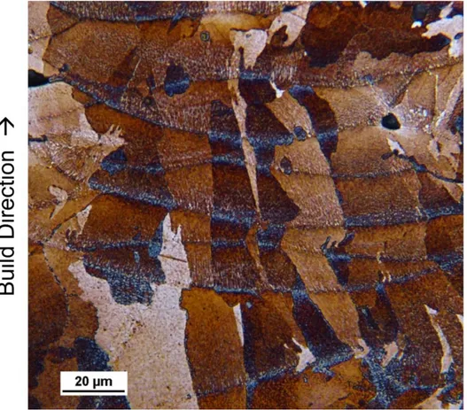
Figure 3 shows the solidification substructure of SLM AlSi10Mg. Cellular solidification substructures dominate in alloys fabricated by SLM. In some cases, as in Figure 3, a very small heat affected zone can be observed that affects the substructure near the weld line. The substructure tends to get finer moving away from the weld line, but the morphology does not change.
20
Figure 3. Change in solidification substructure moving away from the weld line in SLM AlSi10Mg.The build direction is vertical. [24]
Solidification substructures arise from solute rejection and constitutional supercooling during solidification. The substructure scale changes moving away from the weld line due to the changing thermal gradient(G) and
solidification rate(R) in the weld pool and is a well understood phenomenon from welding metallurgy.[33] In casting the substructure tends to predictably change as G changes. In welding and SLM where there is a moving heat
21
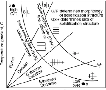
source, the situation becomes somewhat more complicated as R is related to the heat source travel speed and varies with the location in the weld pool. Figure 4 shows a diagram of the predicted substructure features at different G and R conditions. The ratio of G/R dictates the type of solidification
substructure, while the product of GxR (the cooling rate) defines the scale of the substructure. At the weld centerline GxR is minimum at the centerline of the melt pool and maximum at the fusion line. Therefore, further away from the fusion line the substructure is predicted to become finer.[33] This occurs in SLM aluminum alloys as shown in Figure 3. In welding processes, G/R ratio typically changes enough to cause changes in the solidification substructure throughout the weld pool but this does not appear to be the case in standard SLM of aluminum and ferrous alloys.[24, 30]
Figure 4. Variation in solidification substructure under different G and R conditions.[33]
22
Nearly all metallic alloys currently utilized in SLM exhibit epitaxial growth from the previous build layer resulting in elongated grains in the build direction. Titanium alloys in particular exhibit very large columnar prior β grain boundaries.[29, 34] Texture resulting from directional solidification can be tailored with scanning strategy as shown in aluminum alloy systems.
Unidirectional scanning with no rotation between build layers produces a fairly strong <100> texture in the scan direction and a weaker <110> texture in the build direction. Small increases in complexity of the scan strategy nearly eliminate this texture; bidirectional scanning with rotation between layers only produces a weak <100> texture in the build direction. In parts fabricated using an island scanning strategy, preferred texture is negligible.
In titanium alloys, research has shown that the preferred growth direction of the columnar grains can change when moving from the interior of the component to the edge of the component. Near the edge of the
component grains are nucleated epitaxially from loose powder particles. Although this mechanism can occur in the center of the bulk part, the grains are typically re-melted and are indistinguishable from grains that epitaxially grow from underlying bulk material. Near the edge however, the grain structure can remain resulting in a distinct change in texture in near surface layers. [34] For very deep melt pools, competitive growth could occur along the melt pool wall, but epitaxial growth still dominated near the weld
23
Several grain nucleation mechanisms exist in the weld pool and their effect is pronounced in single-track experiments, which are conceptually very similar to traditional welding metallurgy.[33] In bulk SLM materials, the dominant grain formation mechanism is nearly always epitaxial growth due to the significant re-melting of previously solidified material. The effect is clearly shown by electron backscatter diffraction in the build direction as shown in Figure 5.
Figure 5. Epitaxial growth observed in the weld pools of SLM AlSi10Mg.[24]
In many cases, an isotropic material is desired so the scan strategy is adjusted to attain as close to this condition as possible. This is accomplished most readily by changing the laser scan direction which causes subtle
changes in the solidification direction that minimize texture. However, recent findings suggest that with careful control of the shape of the laser spot,
24
different grain growth mechanisms can be activated. In particular, it was found that in stainless steel the solidification mode can be shifted from columnar dendritic to equiaxed dendritic to achieve some degree of an equiaxed grain structure. The study was limited to single track melt pools and further research is needed to fully develop the technique for bulk components.[22] Alternatively, there is some interest in utilizing this observation to create engineered texture in components.[32] SLM investigations of NiTi alloys have found that texture, grain size, and to some degree grain shape can be controlled by changing the weld pool characteristics via laser parameters. Multiple scanning of a single build layer can lead to further tuning of texture, but grain growth is typically observed due to reheating. [35]
Mechanical property differences between SLM and wrought materials are fairly well understood for the most popular alloys. General trends will be described here, but the presence of defects in SLM parts remains an issue in reproducibility and reliability of measured properties. Yield strength and
hardness are typically higher than wrought counterparts as a result of the high cooling rate. In contrast, ductility is consistently lower than wrought
counterparts due to the presence of porosity and cracking from
processing.[36, 37] Vrancken et al. also demonstrated that in the case of Ti-6Al-4V conventional mill heat treatments do not produce optimum mechanical properties when applied to SLM components.[38, 39] This is particularly important in alloys that are strengthened via post-processing heat treatments
25
which is common in SLM since no cold deformation is imparted in the
traditional sense during fabrication. Precipitation hardening SLM nickel alloys also have unique response to heat treatment compared to their wrought counterparts. SLM Inconel 718 requires a higher solution treatment
temperature after processing because the high cooling rate during processing leads significant microsegregation and metastable phase formation. Longer solution treatments at higher temperatures are required to return the material to a desirable homogeneous supersaturated solid solution prior to aging. Additionally, heavy elements in nickel alloys like molybdenum can segregate strongly, leading to high concentrations of defects in the interdendritic regions. The defects in the interdendritic region lead to a microsegregation of
precipitates if solution treatment was not conducted at a high enough temperature. [40]
Anisotropy of mechanical properties is present to varying degrees depending on material texture and residual stresses, and typically manifests as different properties in the build direction as compared to the X-Y plane. As expected, fatigue performance of SLM components is generally worse than wrought counterparts as a result of microstructural defects and residual stresses at the surface of SLM components.[41]
Residual stresses resulting during SLM are highly complex and depend on the processing parameters, part geometry, and the material properties. Current work from the University of Leuven on SLM components focuses on
26
type I residual stresses (macro-stresses). Due to the significant effect of process parameters on residual stress, it is very difficult to isolate material property effects because different parameters are needed to produce a fully dense part. In terms of geometry, the larger the part is in the build direction, the higher the maximum residual stress in the component. Along the build direction, the general trend of the residual stress is a small zone of tensile stress at the top and bottom of the part, with a broad zone of compressive stress in the center of the build. In the X-Y plane, tensile stress is generally present on the outside surfaces and internally stresses are larger in the direction of the scan. Thus, residual stresses in the X-Y plane can be significantly reduced by shortening the maximum scan vector length and scanning in different directions between layers/islands. In general, parts removed from the baseplate or built on a support structure to allow for some relaxation during fabrication have much lower residual stress in the build direction than parts still affixed directly to the base plate. Therefore, type I residual stresses can be somewhat mitigated by scan strategy and the presence of a support structure.[39, 41]
2.3 The Physical Metallurgy of Copper Alloys
2.3.1 Overview of Copper AlloysCopper has the highest electrical conductivity of any commercial metal; it is surpassed only by silver which is prohibitively expensive for use in
27
produced are destined for electrical or heat transfer applications. These
applications include electrical connectors, electrical wiring and heat exchanger assemblies. For applications that do not require high strength, oxygen-free and “tough pitch” coppers are used. Although these alloys have a conductivity around 100% International Annealed Copper Standard (IACS), they are limited by their mechanical strength, with a maximum ultimate tensile stress of ~395 MPa. In practice, many applications necessitate the use of copper alloys with higher strength so understanding the mechanical properties of copper alloys destined for electrical applications is vitally important. However, the main strengthening mechanisms in metals have a detrimental effect on conductivity. Figure 6 shows the conductivity vs ultimate tensile strength for some common commercial copper alloys demonstrating this trade off. [16] This chapter will briefly discuss the main strengthening mechanisms in common copper alloys, their effect on conductivity, and their relevance to the SLM process. Following these sections the two alloys investigated in this research, Cu-4.3Sn and C70250, will be introduced. The binary tin bronze alloy is not a commonly studied composition commercially nor in literature and thus a general introduction to single phase tin bronze alloys is presented rather than a literature review. In the case of C70250, a review of current literature on the alloy in wrought form is presented. Chapters 3 and 4 will individually address metallurgy concepts as they relate to the performance of the SLM fabricated alloys characterized in this investigation.
28
Figure 6. Conductivity vs. ultimate tensile strength for various annealed copper alloys. [16]
2.3.2 Introduction to the Conductivity of Copper Alloys
Conduction in metals results from the movement of free electrons through the crystal structure. Electrical conductivity (σ) is therefore
proportional to the mobility of free electrons. Defects and impurities in alloys that scatter electrons moving through the lattice decrease the conductivity by decreasing the mean free path of electrons. Often, the electrical behavior of metals is discussed in terms of their resistivity (ρ), the geometry-independent form of electrical resistance, measured in Ωm. Electrical resistivity is related to the conductivity through a simple inverse relationship (σ=1/ρ). Matthiessen's Rule (Equation 1
𝜌 = 𝜌
𝑟+ 𝜌
𝑡) states that the total resistance of a metal is the29
sum of a residual component due to defects, and a thermal component due to thermal vibrations.
𝜌 = 𝜌
𝑟+ 𝜌
𝑡 Equation 1For most metals, the resistivity is proportional to temperature related by the temperature coefficient of resistivity (TCR). The TCR of metals is a positive value, leading to an increase in resistivity with increasing temperature due to increased electron scattering from thermal lattice vibrations.[43] Since copper has an inherently low resistivity, contributions to the residual resistivity from defects and impurities will have a significant effect on the total resistivity of copper alloys.[44] Throughout the next section where the major strengthening mechanisms of copper alloys are discussed, their effect on total resistivity (via the residual resistivity term) will also be mentioned.
2.3.3 Principle Strengthening Mechanisms of Copper Alloys 2.3.3.1 Work (Strain) Hardening
Deforming a metal/alloy plastically causes an increase in the number of dislocations in the material. The number of dislocation-dislocation interactions then also increases and the dislocation mobility is reduced, which in turn
causes the required stress for continued deformation to rise. The accumulation and storage of dislocations is thus the basis for work hardening an alloy (note the terms work hardening, strain hardening, and cold working all refer to the same phenomenon). Applying a higher strain to the same material, and thus increasing the number of dislocations introduced and stored in the material,
30
increases the flow stress (i.e. the new yield stress after unloading) so that the degree of work hardening is related to the amount of increase in yield strength. This process strengthens alloys when deformation is done at temperatures below a critical value of around 0.3Tm. Above this critical temperature, the
microstructure is unstable and recovery, recrystallization, and grain growth processes can occur leading to nucleation of low dislocation density grains counteracting the work hardening effect.[45]
The way an alloy responds during work hardening can be characterized by analyzing the plastic regime of a stress strain curve. On the microstructural scale, work hardening is divided into several stages corresponding to different dislocation behavior that occur as deformation progresses. The stages are characterized by the slope of the true flow stress vs. plastic strain plot after yielding which is the work hardening rate (Θ). In single crystal samples, all stages are generally observed; however, in polycrystalline samples it is
common for the material to only exhibit Stage III hardening after an initial large hardening rate at small strains that is independent of strain rate (Stage II). Stage II is athermal occurs near the yield point, but the extent of observation of Stage II work hardening in polycrystalline samples depends on the test temperature and stacking fault energy of the material (i.e. Stage III begins and affects observation of Stage II).For this reason, it is difficult to precisely define the transition from Stage II to Stage III and Stage II is currently considered more of an asymptotic work hardening rate at low strain values.[46] Stage III is
31
characterized by dynamic recovery processes and the work hardening rate during this stage varies with temperature and strain rate. From a practical standpoint, Stage III describes most of the regime where materials are being work hardened (with the near yield Stage II that is transient describing the initial low strain portion). The simplest differential strain-hardening law, the Voce relation, is fairly accurate for polycrystals and an improvement over simple power law relations. The Voce relation describes a linearly decreasing work hardening rate with an increasing stress. The differential version of the Voce relation is shown in Equation 2.
𝛩 =
𝜕𝜖𝜕𝜎𝑝
= 𝛩
0∙ (1 −
𝜎−𝜎𝑌𝜎𝑠−𝜎𝑌
)
Equation 2Where 𝜎 is the true stress, 𝜖𝑝is the plastic strain, Θ0 is the initial work
hardening rate, 𝜎𝑌is the yield strength and 𝜎𝑠 is the saturation stress. Figure 7
shows a schematic diagram of the work hardening rate versus stress with the Voce equation parameters indicated on the axes. Curves a and b are for different strain rates and serve to indicate that tests at different strain rates will produce different relations even if the material has the same yield strength.[47] Note that the bottom of the curves do not actually reach the saturation stress due to the activation of higher order work hardening stages that are not fully understood. The linear approximation works very well for FCC metals that are either pure or solid solution strengthened (discussed later in this chapter) because the dislocation accumulation mechanisms are the same. However, in multiphase systems, there is deviation from the linear nature of the curve due
32
to dislocation interactions with the second phase and this can be utilized to infer some information about the morphology of the second phase.[47, 48]
Figure 7. Work hardening rate (𝛩) versus stress (𝜎) for different strain rates (a and b) with the Voce parameters specified on the axes.[47]
Copper and its alloys have good work hardening behavior and are readily cold worked in excess of 90% reduction in area as a finishing step to improve properties for commercial applications.[16, 44] Work hardening is especially utilized in pure copper where the low recrystallization temperature limits the applicability of Hall-Petch strengthening due to grain growth at moderate temperatures. Work hardening only decreases the conductivity of copper alloys by at 1-3% IACS, however it can improve their strength
substantially. The dislocations introduced from deformation shorten the mean free path of electrons, but the effect is minimal.[43]
Work hardening is not available as a strengthening mechanism directly in the SLM process. Similar to casting, SLM is a near-net-shape solidification
33
process; there is no inherent deformation involved that would provide work hardening without the addition of a post-processing step. However, there is a significant amount of residual stress generated during solidification in SLM that can lead to a high dislocation density structure providing a somewhat similar strengthening effect.[42] Additionally, work hardening behavior can be utilized to understand the mechanical response of alloys produced via SLM,
particularly in the case of understanding the morphology of second phase precipitates.[49]
2.3.3.2 Hall-Petch Strengthening (Grain Boundary Strengthening)
Just as adding barriers to dislocation motion in the form of more dislocations increases the yield strength in work hardening, grain boundaries serve as an effective barrier for dislocation motion and increase strength. Dislocations cannot easily slip across a grain boundary because the crystal structure is different in the second grain and the grain boundary results in a discontinuity of the slip planes in each grain. The relationship between yield strength (𝜎𝑦) and grain size (d) is described by the Hall-Petch equation (Equation 3).
𝜎
𝑦= 𝜎
0+
𝑘𝑦√𝑑
Equation 3
Where 𝜎0 and 𝑘𝑦 are constants that vary based on the alloy and are generally related to the lattice resistance to dislocation movement and the relative hardening of grain boundaries, respectively. Although some alloys do not follow the Hall-Petch equation to very small grain sizes, copper alloys have
34
been found to adhere to Equation 3 down to around 10 nm.[50] Traditionally manufactured wrought copper alloys, particularly high strength copper alloys, are regularly hot worked to refine the grain structure and increase strength per the Hall-Petch relationship.
Andrews et al. was able to measure the contribution of grain boundaries to resistivity in polycrystalline copper and aluminum. They found that the
specific grain boundary resistivity was independent of impurity content, and had a small dependence on temperature. They determined that the increase in resistivity attributed to grain boundaries (Δρgb) could be described by Equation
4.[51]
∆𝜌
𝑔𝑏=
23
𝜌
𝑠𝑔𝑏(
𝑆𝑉
)
Equation 4Where the specific grain boundary resistivity, ρsgb, is equal to 3.12×10⁻¹⁶ Ω m2.
S/V is the grain boundary surface area to volume ratio for a grain with diameter, d. S/V~ 2.37/d using the assumption that the grains are tetradecahedral.[50] Using Equation 2 and the S/V approximation, an estimation of the contribution to resistivity can be determined for a range of grain diameters. The grain boundary contribution to resistivity is negligible for grain sizes above around 1 µm. Although some unique processing methods exist to produce nano-grained copper alloys, common grain sizes are far above this threshold and thus contributions from grain boundary resistivity is usually ignored.
35
Current SLM research indicates that there is some degree of control over grain nucleation and growth which affects the final grain size. Laser parameters and intensity profiles have been altered for aluminum, nickel-titanium, and stainless steel alloys to control the grain size and texture with some degree of success.[22, 24, 35]. Additionally, changes in alloy
composition have the capability to introduce inoculants that promote
heterogeneous nucleation and limit the amount of epitaxial growth that occurs during solidification. In particular, this phenomenon has been proven effective in scandium modified aluminum alloys. This mechanism was proven with pre-alloyed powder, although in principle the amount of inoculant could be varied by mixing two different powders to vary the composition during each
production run.[51, 52] In practice, however, the grain size of alloys produced via SLM is essentially fixed. Commercial applications utilize a set of ideal parameters based on density experiments performed either internally or by the machine manufacturer. In the latter case, the “optimum” parameters are
supplied to owners of the machine but in both scenarios the parameters are normally held constant after optimization. Therefore, the contribution to strengthening from grain size is fixed in the as-printed condition. Post-processing heat treatments could potentially alter the grain size via
recrystallization directly from the as-printed structure. Studies on post-SLM heat treating and hot isostatic pressing (HIP) generally indicate that grain refinement directly from the as-printed condition is not possible and in fact
36
grain growth occurs that decreases strength per Equation 3. Investigated alloys include Ti-6Al-4V, steel, and Al-12Si; these studies demonstrate
significant coarsening of microstructural features during post-processing heat treatment.[53-55]
2.3.3.3 Solid Solution Strengthening
Work hardening and grain refinement can strengthen pure metals and alloys alike. However, adding solute atoms to a pure metal while retaining a single phase results in an alloy that is solid solution strengthened. Solute atoms with a different atomic radius than the matrix produce distortion in the surrounding lattice. These distortion fields interact with dislocations making it more difficult for dislocations to move through the lattice thereby increasing strength. The amount of strengthening depends primarily on the relative size difference of the solute/matrix atoms, the stress field associated with the solute in the lattice, and the amount (concentration) of solute atoms in the matrix.[45] Many of the most ubiquitous copper alloys utilize solid solution strengthening. Figure 8 shows the approximate strengthening effect of various solute atoms in an FCC copper matrix at room temperature.[16] Two of the most common solid solution strengthened alloys are phosphor bronze, Cu-Sn alloys, and brass, Cu-Zn alloys. A note on copper alloy nomenclature:
technically a bronze is copper plus any other alloying element; for example “aluminum bronzes” are Cu-Al alloys, but the use of bronze without an elemental descriptor was traditionally used to refer to Cu-Sn alloys. In
37
contemporary usage, “phosphor bronze” refers to modern Cu-Sn alloys that have been phosphor de-oxidized, despite the fact that Sn is the principal alloying element. Brass, however, is still used to exclusively refer to copper alloys where Zn is the primary alloying element (even if other elements are present in smaller amounts). Sn and Zn have relative atomic diameter differences compared to copper of -15% and -4%, respectively. Examining Figure 8, the difference in strengthening potential as a result of the size effect is evident. The strengthening effect has influences outside atomic radius difference, but Sn and Zn are both substitutional lattice impurities so in this case the atomic size difference is dominant. Sn has a much higher
strengthening potential than Zn, despite the fact that much more Zn (around 35%) can be dissolved in the copper matrix compared to Sn (around 10% solubility in practice). However, Zn has a very good combination of solubility and strengthening effect and brass alloys are the most commonly used copper alloys. Cu-Sn alloys are more commonly utilized when high strength and good wear resistance is required.[16]
38
Figure 8. Approximate effect of solute content on the critical resolved shear stress at room temperature.[16]
In simplified/colloquial language, one may say that how well a solute atom “fits” in the native copper matrix determines the degree of the solid solution strengthening effect of that atom. Unfortunately, the same is true for how detrimental a solute atom will be to the conductivity of copper by
scattering free electrons. In other words, elements that are good solid solution strengtheners in copper also increase the resistivity significantly. The amount of resistivity increase is controlled by similar variables as solid solution
strengthening: amount, atomic radius, crystal structure and electronegativity among other factors.[43] Amongst the strengthening methods utilized in
![Figure 5. Epitaxial growth observed in the weld pools of SLM AlSi10Mg.[24]](https://thumb-us.123doks.com/thumbv2/123dok_us/1409271.2688620/38.918.229.729.367.768/figure-epitaxial-growth-observed-weld-pools-slm-alsi.webp)

![Figure 8. Approximate effect of solute content on the critical resolved shear stress at room temperature.[16]](https://thumb-us.123doks.com/thumbv2/123dok_us/1409271.2688620/53.918.339.617.120.595/figure-approximate-effect-solute-content-critical-resolved-temperature.webp)
![Figure 9. The effect of small additions of solute atoms on the resistivity of copper.[58]](https://thumb-us.123doks.com/thumbv2/123dok_us/1409271.2688620/55.918.281.683.156.578/figure-effect-small-additions-solute-atoms-resistivity-copper.webp)
![Figure 10. Schematic diagram of the major strengthening mechanisms active during a precipitation hardening aging heat treatment.[45]](https://thumb-us.123doks.com/thumbv2/123dok_us/1409271.2688620/58.918.298.683.118.444/figure-schematic-diagram-strengthening-mechanisms-precipitation-hardening-treatment.webp)