International Journal of Electrical & Computer Sciences IJECS-IJENS Vol:17 No:05 1
163605-8282-IJECS-IJENS © October 2017 IJENS I J E N S
Low Power Optimization Technique and a genetic
minimization algorithm for variable ordering of BDD mapped
VLSI Circuits
Manu Bansal, Alpana Agarwal
Abstract— Ordered binary decision diagrams (BDDs) yield a data structure for switching functions that has been proven to be very useful in sloving many of the problems in VLSI CAD. BDD-based calculations is the variable ordering problem which addresses the major problem of finding an ordering of the input variables which minimizes the size of the BDD-representation. In this paper, the use of genetic algorithms to improve the variable ordering of a given BDD is implemented and experimental studies are reported. This paper proposes genetic algorithm with three crossover operators namely order, cycle and partially mapped (PMX) crossovers for minimization of shared ordered Binary Decision Diagrams (BDDs). The implementation was done using C++ codes and the simulation was carried out on the BUDDY 2.4 package on Ubuntu 12.04. The observations for the node count show that the node count reduction, maximum 74% (for 8-adder) is better obtained by using PMX operators both for the LGSynth93 benchmark circuits as well as multi-input adders. The power estimation was done for the circuits and a maximum of about 99.9% power reduction has been obtained by the proposed technique in case of Multi-input adders, especially in case of 6-adder and 8-adder. The proposed Genetic algorithm is found to be suitable for multi-input multi-output (MIMO) VLSI circuits.
Index Term— Genetic Algorithm, BDDs, Order, Cycle,
Partially Mapped.
I. INTRODUCTION
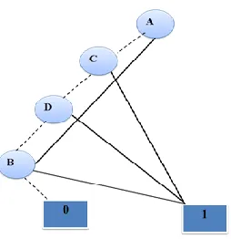
Binary Decision Diagrams (BDDs) [1-3] are the data structures that are used for compact representation of Boolean functions. BDD is a finite directed acyclic graph (DAG) with a unique initial node as shown in figure 1. Every non-terminal node is marked by a Boolean variable. There are exactly two edges, labelled 0 and 1, from one non terminal node to other nodes. Shannon decomposition is carried out for each node. The need of the time is that we need to optimize chip area usage to increase its functionality.
A good variable order is needed that minimizes the size. In this paper, genetic algorithm with three versions of the crossover operator has been used for BDD minimization: Order Crossover, Partially Mapped Crossover and Cycle Crossover.
II. GENETIC ALGORITHM FOR BDD REDUCTION Genetic Algorithms (GA), [4, 10] are a family of excellent optimization techniques based on Darwinian Theory. The objective of GA is to find an optimal ordering of BDDs with reduced node count and computation time. GAs work by finding a best individual i.e. BDD ordering from a population of individuals evolved over many generations. A fitness value i.e. in terms of node count is assigned to each individual i.e. BDD order. A population of random individuals is initialized. Parents are selected based on their fitness values and crossover
Fig. 1. Binary Decision Diagram for the function F=AB + A’C + BC’D
and mutation operations are performed on them to generate offspring with a better fitness value i.e. node count. The process is continued till an optimum solution i.e. BDD with least node count is found.
III. CROSSOVER OPERATORS FOR GENETIC ALGORITHM
Crossover [5] is an important step in the genetic algorithm. The crossover operator strongly affects the performance of genetic algorithm. Three versions of the crossover operator have been used for BDD minimization:
3.1.Order Crossover (OX): It was proposed by Davis and also used for chromosomes with permutation encoding. Order crossover applies sliding motion to fill up the left out holes by sending the mapped positions. The elements on left hand side of crossover point of parent 1 are directly copied to offspring at same positions. The remaining fields of the offspring are filled by the elements of parent 2 in order, leaving the ones which have already been taken up from parent.
International Journal of Electrical & Computer Sciences IJECS-IJENS Vol:17 No:05 2
163605-8282-IJECS-IJENS © October 2017 IJENS I J E N S
Accordingly they are exchanged in parent 1 to form a new individual.
3.3.Cycle Crossover (CX): This crossover is used for chromosomes with permutation encoding. During recombination in cyclic crossover there is a limitation that each gene either comes from the one parent or the other. The fundamental model at the back cycle crossover is that each allele comes from one parent jointly with its position. Every cell in offspring occupies position similar to either of the two parents.
IV. PROPOSED ALGORITHM/ FLOWCHART for BDD MINIMIZATION
This algorithm takes a population size and number of iterations is fixed at 50 chromosomes per generation with 80% crossover rate and 4% mutation rate. The generation size begins with 20 generations and constants δ1, δ2, γ1, and γ2 as given in [14] have been fixed at 10%. The constant µ for change in mutation rate is set as 0.05.
A complete proposed algorithm is explained below:
1. Initialize a new random population of BDDs for a benchmark circuit.
2. Calculate individual fitness i.e. node count for each BDD.
3. Apply Crossover Operator (Order / PMX / Cycle) i.e. combine features from two different parent a new placement.
4. Apply Mutation i.e. modify characteristics of existing solution to generate a new one with number of mutations not more than number of elements/2+1. 5. Is the solution consistent? If no go to step 3 and if yes
go to step 6.
6. Calculate the node count and power.
V. SWITCHING ACTIVITY ESTIMATION
The minimization of power consumption is an important design constraint for circuits used in portable devices [11, 12]. The s itching activity of a circuit node in a CMOS digital circuit directly contributes to overall power dissipation. By approximating the switching activity of circuit nodes as internal switching probabilities in Binary Decision Diagrams BDDs), it is possible to estimate the dynamic power dissipation characteristic of circuits resulting from a structural mapping of a BDD. The power dissipation of each node of the binary decision diagram is computed by the estimated switching activity and the fan out of the node. A BDD is directly mapped to a multiplexer-based circuit and the resulting circuit is obtained by replacing BDD vertices with small sub circuits and BDD edges with wires. The diagram size (and therefore the circuit complexity) is sensitive to the ordering of the function variables. The complexity varies from linear to exponential under different orderings for some functions. The power dissipation of each node is computed by the estimated switching activity and the fan out of the node. The variable order of the underlying BDD influences not only the area (number of nodes) but also the internal switching activity. The technique is also used with BDDs using
complemented edges. The use of complemented edges is shown to both reduce BDD complexity and improve performance of operations.
1. The output probability, P (f -), of f - is equal to 1-P (f). 2. The switching activity, a (f -), of f -is equal to a (f).
A cost model based on the total circuit switching activity under a given set of dependent-variable output probabilities is defined. The dependent variables are denoted as support variables. The sum of all internal switching activities at each BDD vertex is minimized. Each BDD node is then mapped into a multiplexer-based circuit. The number of stages of active buffers is determined by the fan out of each BDD node, which is equivalent to the number of BDD edges pointing to the node. The power dissipation for the mapped node PDn is estimated using the relationship in (1):
PDn = a(n) x driver(fan out (n)) + leakage(n) (1)
In (1), the power dissipation due to leakage is ignored as its contribution to total power dissipation is very less; therefore, leakage (n) is ignored.
VI. SIMULATION RESULTS
The Proposed Genetic algorithm, using three types of crossover operators, is implemented with C++ codes and simulated using BUDDY 2.4 package on Ubuntu 12.04. In this section, simulation results i.e. node count and power for LGSynth93 benchmark circuits and Multi-input Adders has been presented in Table I, II, III, and IV.
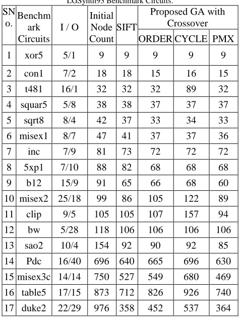
Table I
Comparison of Node Count for Dynamic and Genetic algorithms for LGSynth93 Benchmark Circuits.
SN
o. Benchmark
Circuits I / O
Initial Node Count SIFT
Proposed GA with Crossover
ORDER CYCLE PMX
1 xor5 5/1 9 9 9 9 9
2 con1 7/2 18 18 15 16 15
3 t481 16/1 32 32 32 89 32
4 squar5 5/8 38 38 37 37 37
5 sqrt8 8/4 42 37 33 34 33
6 misex1 8/7 47 41 37 37 36
7 inc 7/9 81 73 72 72 72
8 5xp1 7/10 88 82 68 68 68
9 b12 15/9 91 65 66 68 60
10 misex2 25/18 99 86 105 122 89
11 clip 9/5 105 105 107 157 94
12 bw 5/28 118 106 106 106 106
13 sao2 10/4 154 92 90 92 85
14 Pdc 16/40 696 640 665 696 630
15 misex3c 14/14 750 527 549 680 469
16 table5 17/15 873 712 826 926 740
International Journal of Electrical & Computer Sciences IJECS-IJENS Vol:17 No:05 3
163605-8282-IJECS-IJENS © October 2017 IJENS I J E N S Table II
Comparison of Node Count for Dynamic and Genetic algorithms for Multi-Input Adders.
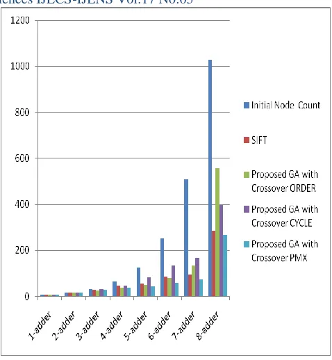
Fig. 2. Comparison of Node Count for different LGSynth93 Benchmark Circuits using different Algorithms.
VII. CONCLUSION
It is observed that in comparison with other existing algorithms, the proposed GA technique gives minimum node count. Also, when the crossover operators are compared, Partially Mapped Crossover gives minimum nodes for most of the circuits. The order crossover also gives optimum results. TableI shows that the node count for multi-input and single-output circuits i.e. xor5 benchmark circuit and t481 benchmark circuit is same for the entire existing as well as proposed algorithm. For multi- input and multi-output circuits the reduction number of node count is tremendous. As inputs keep on increasing the reduction in node count keeps on increasing. For 5xp1 benchmark circuit the reduction is about 22.7%, b12 benchmark circuit is about 34%, for multi- input and multi-output circuits where the number of outputs are equal or more than the number of inputs, the reduction in the node count is not considerable. For squar5 benchmark circuit the node count reduction is about 2.6%, pdc benchmark circuit is about 9.4%. In multi-input adder circuits, as number of inputs are increasing, the proposed genetic algorithm with PMX crossover gives best reduction in node count. From Table II, for 1-adder, with crossover reduction in node count is
Fig. 3. Comparison of Node Count for multi-input adder circuits using different algorithms.
about 0%, for 2-adder is about 0%, for 3-adder is about 18.75%, for 4-adder is about 44.44%, for 5-adder is about 65.07%, for 6-adder is about 77.07%, for 7-adder is about 85.82% and for 8-adder is about 74%. Therefore, the proposed Genetic algorithm is suitable for multi-input multi-output (MIMO) VLSI circuits.
In case of the estimation of power dissipation, it is observed that that in more than 90% cases, proposed algorithm based approach using probabilistic analysis has shown lesser power dissipation than the Multiplexer based existing technique. From table II, it can be concluded that the power dissipation in case of PMX and Order Crossover Operators is lesser than Cycle Crossover Operator in case of genetic Algorithm for 80% benchmark circuits. Moreover about 99.9% power reductions have been achieved for the 6-adder and 8-adder Multi-input adders with the proposed Genetic Algorithm. Experimental results on a set of multi – input adders and LGSynth93 benchmarks show the estimated reduction in power dissipation.
The proposed genetic minimization algorithm iteratively seeks a variable order that reduces the mapped circuits' switching activityweighted by the fan-out cost for each node.
VIII. OVERVIEW OF BDD PACKAGE
A BDD package[15, 16] has three main components: the BDD algorithm component, the dynamic variable ordering component and the garbage collection component. The common features of these components are described as under:
1. BDD Algorithm
This component computes the resultant BDDs for different Boolean functions. The implementation of these algorithms is typically based on depth-first traversal. The unique tables are hash tables with the hash collisions resolved by chaining. A SNo.
Benchmark Circuits
I/O
Initial Node Count
SIFT
Proposed GA with Crossover
ORDER CYCLE PMX
1 1-adder 3/2 8 8 8 8 8
2 2-adder 5/3 17 17 17 17 17
3 3-adder 7/4 32 26 25 32 26
4 4-adder 9/5 63 46 35 45 35
5 5-adder 11/6 126 55 49 82 44
6 6-adder 13/7 253 85 79 132 58
7 7-adder 15/8 508 94 135 165 72
International Journal of Electrical & Computer Sciences IJECS-IJENS Vol:17 No:05 4
163605-8282-IJECS-IJENS © October 2017 IJENS I J E N S Table III
Comparison of Power for probabalistic technique in Genetic algorithms with existing techniques on various crossovers for LGSynth93 Benchmark Circuits.
SNo. Benchmark
Inputs / 0utputs
Power using Probabilistic Tech in GA with crossover
Power using MUX Approx. in GA with crossover
Order(mW) PMX (mW) Cycle (mW) Order(mW) PMX (mW) Cycle (mW)
1 b12 15/9 0.0001212 0.00335 0.0000257 0.050312 0.051837 0.045738
2 5xp1 7/10 0.0000619 0.0018819 8.002E-05 0.051837 0.051837 0.051837
3 bw 5/28 0.0733 0.00000976 0.0000098 0.080805 0.080805 0.080805
4 con1 7/2 0.0062263 0.01172 0.01172 0.011434 0.012197 0.0114346
5 inc 7/9 0.000152 0.000697 0.000697 0.054886 0.054886 0.054886
6 sqrt8 8/4 0.00005227 0.003183 5.447E-05 0.025156 0.0259186 0.0251563
7 xor5 5/1 0.8666 0.8666 0.8666 0.00686 0.0686 0.0686
8 pdc 16/40 0.00000836 0.000931 4.39E-06 0.506938 0.530569 0.480256
9 duke2 22/29 0.0003491 0.000636 0.0001 0.0003491 0.000636 0.0001
10 misex1 8/7 0.000010091 0.0004334 0.0008188 0.028205 0.028205 0.028205
11 misex3c 14/14 0.00361 0.0919 0.00696 0.41851 0.518372 0.357524
12 table5 17/15 0.0001011 0.000914 0.0000369 0.0001011 0.000914 0.0000369
13 t481 16/1 0.0000086 0.00005447 3.15E-06 0.024394 0.067845 0.024394
14 squar5 5/8 0.000314 0.000314 0.000314 0.028205 0.028205 0.028205
15 clip 9/5 0.0000654 0.00000453 2.356E-06 0.081567 0.119683 0.071657
16 sao2 10/4 0.00000431 0.00000765 1.23E-06 0.068608 0.070132 0.064796
Table IV
Comparison of Power for probabalistic technique in Genetic algorithms with existing techniques on various crossovers for Multi-Input Adders.
SNo. Benchmark
Inputs / Outputs
Power using Probabilistic Tech in GA with crossover
Power using MUX Approx.in GA with crossover
Order(mW) PMX (mW) Cycle (mW) Order(mW) PMX (mW) Cycle (mW)
1 2-adder 5/3 0.003361 0.003361 0.003361 0.012959 0.012959 0.012959
2 3-adder 7/4 0.01661 0.00463 0.004661 0.019057 0.024394 0.01982
3 4-adder 9/5 0.002301 0.002387 0.003211 0.02668 0.034304 0.02668
4 5-adder 11/6 0.01611 0.027512 0.0254987 0.037353 0.062509 0.033541
5 6-adder 13/7 0.021876 0.000134 0.000231 0.060222 0.100625 0.044214
6 7-adder 15/8 0.006341 0.00812 0.001223 0.102912 0.125781 0.054886
International Journal of Electrical & Computer Sciences IJECS-IJENS Vol:17 No:05 5
163605-8282-IJECS-IJENS © October 2017 IJENS I J E N S Fig. 4. Comparison of Power for probabalistic technique with MUX Approx. technique on various crossover operators for LGSynth93 Benchmark Circuits.
Fig. 5. Comparison of Power for probabalistic technique with MUX Approx.techniques on various crossover operators for Multi Input Adders.
International Journal of Electrical & Computer Sciences IJECS-IJENS Vol:17 No:05 6
163605-8282-IJECS-IJENS © October 2017 IJENS I J E N S
Manu Bansal received her master’s degree in Electronics and Communication at Thapar Institute of Engineering & Technology, Patiala (Deemed University) in 2003. She works now as Assistant Professor in Electronics & Communication Engineering Department at Thapar University, Patiala. Her research interests are CAD for VLSI, Digital VLSI Design, and Behavioral Modeling for different application fields.
Dr Alpana Agarwal received her MTech Degree in Solid State Materials from IIT, Delhi in 1988 and PhD Degree at Thapar University, Patiala in 2010. She is employed as Associate Professor and Head of Electronics & Communication Engineering Department at Thapar University, Patiala. Her research interests are VLSI Design, Design Automation, ASIC Design, Low Power Low Noise VLSI Circuit Design.
separate unique table is associated with each variable to facilitate the dynamic-variable-reordering process. The computed cache is a hash-based direct mapped (1-way associative) cache. BDD nodes support complement edges where for each edge, an extra bit is used to indicate whether or not the target function should be complemented. The advantage of this encoding is that a function and its complement can be represented by the same BDD and use this extra bit in the reference edge to interpret the BDD either in the positive or the negated form. Implementation-wise, this extra bit is typically encoded in the least significant bit of the address pointer (the reference edge) to avoid incurring extra memory cost. This encoding exploits the property that address pointers in modern machines are always at least 4-byte aligned, which means the least significant bit is always 0. Thus it can be used to encode the complement information.
2. Dynamic Variable Ordering
Since the size of a BDD graph is sensitive to the order selected on input variables, dynamic variable reordering is an essential part of all modern BDD packages. This component aims to dynamically establish a good variable order as the computation progresses. Typically, when a variable reordering algorithm is invoked, all top-level operations that are currently being processed are aborted. When the variable reordering algorithm terminates, these aborted operations are restarted from the beginning. The dynamic variable reordering algorithms are generally based on the sifting algorithm; i.e., the variable orders are changed by exchanging nodes in one level with nodes in the adjacent level.
3. Garbage Collection
BDD computations are inherently memory intensive because after all, it is all about traversing and constructing graphs. Furthermore, in verification, many intermediate BDD results are created to arrive at a simple final answer—true or false. Thus, it is important to have a good garbage collector to automatically remove BDD nodes that are no longer useful. A BDD node is referred to as reachable if it is in some BDD that external user has a reference to. As external users free references to BDDs, some BDD nodes may no longer be reachable (deaths). These nodes are referred to as unreachable BDD nodes. Hence all the unreachable nodes are garbage
collected by the package leading to the fast manipulation and construction of BDDs by reducing the memory requirement.
VIII. REFERENCES
[1] Sheldon B. Akers.Binary Decision Diagrams,IEEE Transactions on Computers, C-27(1978).
[2] R. E. Bryant.Graph-based algorithms for Boolean function manipulation.IEEE Transactions on Computers,35 (1986). [3] F. Towhidi, A.H. Lashkari, R.S. Hossein.Binary Decision Diagram
(BDD).International Conference on Future Computer and Communication(2009) 496-499.
[4] P. W. C. Prasad, A. Assi, A. Harb and V. C. Prasad.Binary Decision Diagrams: An Improved Variable Ordering using Graph Representation of Boolean Functions.International Journal of Computer Science, 1(2006)1-7.
[5] Pinaki Mazumdar,Elizabeth M. Rudnick:Genetic Algorithms for VLSI Design,Layout and Test Automation.
[6] William N.N. Hung, Xiaoyu Song, El Mostapha Aboulhamid, and Michael A. Driscoll. BDD Minimization by Scatter Search IEEE Transactions On Computer Aided Design of Integrated Circuits and Systems, 21 (2006).
[7] N. Zhuang, M.S.T. Benten, and P.Y.K Cheung.Improved Variable Ordering of BDDs with Novel Genetic Algorithm.IEEE International Symposium on Circuits and Systems, 3(1996)12-15. [8] Saurabh Chaudhary, and Anirban Dutta.Algorithmic Optimization
of BDDs and Performance Evaluation for Multi-level Logic Circuits with Area and Power Trade-offs. IEEE International Conference on Electronics, Circuits and Systems,(2011).
[9] Misagh Takapoo, and M.B Ghaznavi-Ghoushchi.IDGBDD: The novel use of ID3 to improve Genetic algorithm in BDD reordering.International Conference on Electrical Engineering / Electronic Computer Telecommunication and Information Technology,(2010)19-21.
[10] Tom V Mathew: Genetic Algorithm:Report submitted at IIT Bombay.
[11] Per Lindgren, Mikael Kerttu, Mitch Thornton and Rolf Drechsler. Low power optimization technique for BDD mapped circuits. ASP-DAC '01 Proceedings of the 2001 Asia and South Pacific Design Automation Conference.
[12] Mikael Kerttu, Per Lindgren, Rolf Drechsler and Mitch Thornton. Low power optimization technique for BDD mapped finite state machines. ASP-DAC '01 Proceedings of the 2001 Asia and South Pacific Design Automation Conference.
[13] Harsh Arora, Arindam Banerjee, Rahul Roopchand Jidge, " Heuristic Approach to Variable Ordering for Logic Synthesis Engine Design:Algorithmic Insight." International Journal of Circuits and Architectural Design,Vol 1, No.2014.
[14] N. Zhuang, M.S.T. Benten and P.Y.K Cheung, “Improved Variable Ordering of BDDs with Novel Genetic Algorithm,” IEEE International Symposium on Circuits and Systems, vol. 3, pp. 414-417, 12-15 May 1996.
[15] A. Hett, R. Drechsler and B. Becker, "MORE: an alternative implementation of BDD packages by multi-operand synthesis" Design Automation Conference, 16 – 20 Sept, 1996, with EURO-VHDL '96 and Exhibition, Proceedings EURO-DAC '96, European [16] G. Janssen "A consumer report on BDD packages" Proceedings