Stop band continuous profile filter in empty substrate
integrated coaxial line
Darío Gómez1, Héctor Esteban1,∗ ID, Angel Belenguer2, Vicente E. Boria1and Alejandro L.
Borja2
1 Instituto de Telecomunicaciones y Aplicaciones Multimedia, Universitat Politècnica de València, 46022 Valencia, Spain; [email protected]
2 Departamento de Ingeniería Eléctrica, Electrónica, Automática y Comunicaciones, Universidad de Castilla-La Mancha, Escuela Politécnica de Cuenca, Campus Universitario, 16071 Cuenca, Spain; [email protected]
1 2
3 4 5 6 7 8 9 10 11 12 13 14 15
16
* Correspondence:[email protected];Tel.:+34-96-387-7758
SimpleSummary:Astopbandcontinuousprofilefilterisimplementedforthefirsttimeinthenovel emptysubstrateintegratedcoaxiallinetechnology.
Abstract: Substrateintegrated waveguides reducethe losses andincrease the qualityfactor of resonatorsin communicationfiltersw henc omparedw itht raditionalp lanart echnologies,while maintainingtheirlowcostandlowprofilecharacteristics.Emptysubstrateintegratedwaveguides goonestepfurther,removingthedielectricofthesubstrate.Oneofthesetransmissionlinesisthe emptysubstrateintegratedcoaxialline(ESICL),whichaddstheadvantageofbeingatwoconductor structure.Thus,itpropagatesaTEMmode,whichreducesthedispersionandthebandwithlimitation ofotheroneconductoremptysubstrateintegratedwaveguides.Continuousprofilefilters,atthecost ofbeinglongstructures,areveryeasytomanufactureanddesign(usuallynooptimizationisneeded), andtheyarehighlyinsensitivetomanufacturingtolerances.Inthisworkasimplecontinuousprofile filter,withastopbandresponse,isdesignedforthefirsttimeinthenovelESICLte chnology.The influenceofthedesignparametersontheinsertionlossesandfractionalbandwidthisdiscussed.A prototypehasbeensuccessfullymanufacturedandmeasured.Asensitivityanalysisshowsthehigh toleranceoftheproposedstopbandfiltertomanufacturingerrors.
Keywords:Emptysubstrateintegratedwaveguides;emptysubstrateintegratedcoaxialline;ESICL; continuousprofilefilters;stopbandfilters
17
1. Introduction 18
The current growth of wireless communications, due to the increase in voice, video and data
19
services, is causing a growing demand for channels and bandwidth. This is driving the future
20
communication systems towards higher frequencies, evidencing the need for the development of such
21
communications systems. Therefore, the aim is to develop low-cost, high-performance technology
22
suitable for mass production, while at the same time achieving a significant reduction in the volume,
23
weight and cost of telecommunications equipment.
24
Over the last years, a great number of substrate integrated circuits [1] has been developed. These
25
circuits are a compromise between the advantages of classical waveguide technologies, such as high
26
quality factor of resonators and low insertion losses, and the advantages of planar circuits, such as low
27
cost and easy compact integration. The substrate integrated waveguide (SIW) [2] and the substrate
28
integrated coaxial line (SICL) [3], are two proposals of substrate integrated circuits that have been a
29
great advance in this field. Several passive components developed in these technologies, including
30
filters [4,5], antennas [6,7], transitions and tapers [8,9], baluns [10,11], couplers [12,13], power dividers
31
[14], and new transmission lines [3,15–18], have been proposed. But although their quality factor and
32
losses are better than those of the planar circuits, these characteristics can be further improved (without
33
losing compactness and low cost manufacturing) if the dielectric substrate is removed and the waves
34
are allowed to propagate through air.
35
This is the purpose of some empty substrate integrated waveguides that have been recently
36
proposed, such as the Modified SIW (MSIW) [19], the Empty SIW (ESIW) [20], the Air-filled SIW
37
(AFSIW) [21], the Hollow SIW (HSIW) [22], or the Dielectricless SIW (DSIW) [23]. All these new
38
transmission lines are integrated in a substrate and they are low profile, low cost, and with higher
39
quality factor and less losses than the SIW, thanks to the complete or partial removal of the dielectric
40
in the path of the electromagnetic (EM) fields. However, these are one conductor structures, which
41
means that the fundamental mode is dispersive, and with a cut-off frequency greater than zero, which
42
limits the usable bandwidth of microwave devices implemented with such novel technologies.
43
These limitations can be overcome with the use of the empty substrate integrated coaxial line
44
(ESICL). The structure of ESICL was first used in [24] for feeding an antenna, and definitely integrated
45
in a planar circuit in [25], where a transition to a classical planar line (a grounded coplanar waveguide)
46
was proposed for the first time. The ESICL is a two-conductor transmission line, whose cross section
47
is a rectangular coaxial built with the superposition of five layers of printed circuit board, as shown
48
in Figure1. This novel transmission line has been recently proposed, and up to date it has only
49
been applied to the implementation of wide band [25] and narrow band [26] microwave filters with
50
a non-dispersive TEM propagating mode. There is, consequently, many possible applications that
51
remain to be explored for this novel transmission line.
52
One of these possible applications is implementing continuous profile filters. Conversely to
53
conventional microwave filter topologies, where the filtering structure is based on sharp changes in
54
the cross section that produce sharp impedance steps, continuous profile filters use a progressive
55
and smooth variation of the cross section. This continuous variation has the advantage, at the
56
cost of increasing the length of the filter, of providing a structure with much more resilience to
57
manufacturing tolerances. Besides, the continuous profile filters can be easily and accurately designed
58
with well-known techniques such as the ones described in [27] and [28]. All these techniques require
59
that the phase constant is kept constant (for the same frequency) along the propagation direction.
60
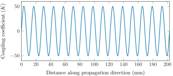
This can be achieved with a structure that propagates a TEM mode (as it is the case of the ESICL), or
61
either with a structure that propagates a non-TEM mode and that varies the cross section along the
62
propagation direction in such a way that the cutoff frequency of this mode does not change. This can
63
be achieved, for instance, varying the height of a rectangular waveguide. If we vary the width of the
64
rectangular waveguide, the cutoff frequency changes and then this is not suitable for the traditional
65
synthesis techniques developed for continuous profile filters. Most one conductor substrate integrated
66
transmission lines (SIW, ESIW, AFSIW, etc.) are H-plane structures, where the width of the rectangular
67
cavity can be changed, but the height is fixed in all the structure (the height of the substrate). Some
68
efforts have been already made to apply the traditional synthesis technique for continuous profile
69
filters in H-plane structures (SIW filter) in [29] and [30]. Although good results are obtained, the
70
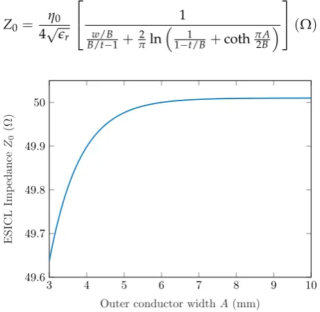
synthesis does not provide so accurate results as when the phase constant does not change along the
71
propagation direction. For that reason, ESICL, with a TEM propagating mode, is an excellent candidate
72
to implement continuous profile filters in substrate integrated waveguide technology (with lower
73
losses than both in planar and classical SIW technologies).
74
In this work a simple continuous profile filter is implemented in ESICL for the first time. The
75
variation of the filter response with the design parameters is studied. A prototype is successfully
76
manufactured and measured, and a sensitivity analysis is performed in order to test the resilience to
77
manufacturing tolerances of this type of filter in this novel transmission line.
2. Materials and Methods 79
2.1. ESICL 80
The ESICL topology can be seen in Figure1. Figure1.(a) shows the five substrate layers needed
81
to manufacture the ESICL. These layers are the top and bottom metallic covers (layers 1 and 5), the
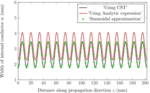
82
central layer with the inner conductor of the ESICL (layer 3), and two more layers that separate the
83
central layer from the top and bottom covers (layers 2 and 4). Layer 3 also hosts the transition from
84
ESICL to the input and output planar accessing lines (coplanar or microstrip).
85
B
A w
t
(a) (b)
Figure 1.Simplest construction of an ESICL (source [25]). Layer 1 and 5 are top and bottom covers;
layer 3 is the central layer with transitions to planar lines; layers 2 and 4 separate central layer from covers.(a)3-D view of layers before assembling.(b)Cross-section of the ESICL after assembling.
The cross section of the ESICL, after the five layers are assembled and pasted with tin soldering
86
paste together, is depicted in Figure1.(b). As it can be observed, after assembling, the cross section is
87
the same as that of a rectangular coaxial line, without any dielectric between the inner and the outer
88
conductors. The dimensions of the cross section are included in the layout. These dimensions are
89
the width (w) and height (t) of the inner conductor, and the width (A) and height (B) of the outer
90
conductor.
91
2.2. Coupling coefficient and impedance 92
As it was already demonstrated in [30], a sinusoidal modulation in the profile of a transmission
93
line produces a stop band filter response. Using the coupled-mode theory, as proposed in [31], a
94
full analytical synthesis can be achieved. To do so, the desired frequency response is used in order
95
to determine the variation of the coupling coefficientK(z)along the propagation direction (z) that
96
provides that response. For complex responses, the coupling coefficientK(z)can be obtained using
97
the zeros and poles of a ideal frequency response expressed as a rational function of polynomials, as
98
proposed in [27]. However, for a simple response as a stop band filter, the coupling coefficient can be
99
directly expressed as a sinusoidal variation of the form [29]:
100
K(z) =Aksin
2π Λz+θ
, z∈[0, np·Λ] (1)
whereAkrepresents the oscillation amplitude,Λis its period,zis the propagation direction, and 101
θis the phase of the sinusoidal.θshould be set to 0 in order to facilitate the subsequent manufacturing 102
process, avoiding sharp changes in the profile at the beginning of the filter.
The value ofΛcontrols the central frequency of the stop band. If we want to locate the center of
104
the stop band at a certain frequency f0, the periodΛshould be: 105
Λ= π
β0 (2)
whereβ0is the phase constant of the propagating mode at the central frequencyf0. 106
The amplitudeAkand the length (or number of periodsnp) of the sinusoidal variation ofK(z) 107
control the depth of the rejection (insertion lossesILatf0) and the fractional bandwidth of the stop 108
band (FBW), as it is described in section2.4.
109
0 20 40 60 80 100 120 140 160 180 200
−50 0 50
Distance along propagation direction (mm)
Coupling
co
efficien
t
(
K
)
Figure 2.Variation of the coupling coefficient (K(z)) along the propagation direction (Λ=13.52 mm,
Ak=50,np=15 andθ=0).
Figure2shows the variation of the coupling coefficientK(z)forΛ=13.52 mm,Ak=50,np=15 110
andθ=0. The value ofΛhas been calculated usingβ0=232.3 rad/m, which is the phase constant 111
of an ESICL withZ0 = 50Ω(A = 6 mm, B = 2.618 mm,t = 0.866 mm andw = 1.8148 mm) at 112
f0=11 GHz. 113
For a device propagating a TEM mode, the relationship between the coupling coefficient and the
114
impedance along the propagation direction is [31]:
115
K=−1 2
1
Z0 dZ0
dz (3)
This equation can be used to express the impedanceZ0as a function of the coupling coefficient as: 116
Z0(z) =Z0(0)e−2
Rz
0K(r)dr (4)
0 20 40 60 80 100 120 140 160 180 200
30 35 40 45 50
Distance along propagation direction (mm)
Imp
edance
Z0
(Ω)
Figure 3.Variation of the impedance (Z0) along the propagation direction.
Substituting the coupling coefficient of Figure2into (4), gives the impedance variation of Figure3.
117
The next step is to obtain an ESICL with a profile that provides this impedance variation.
2.3. Impedance in ESICL 119
The impedanceZ0of an ESICL depends on the dimensions of the cross section (A,B,tandw). 120
The following approximation for the impedance can be found in [32]:
121
Z0= η0 4√er
1 w/B
B/t−1+π2ln
1
1−t/B+cothπ2BA
(Ω) (5)
3 4 5 6 7 8 9 10
49.6 49.7 49.8 49.9 50
Outer conductor widthA(mm)
ESICL
Imp
edance
Z0
(Ω)
Figure 4.Variation of the impedance (Z0) of the ESICL as a function of the outer conductor width.
B=2.618 mm,w=2.2823315 mm,t=0.866 mm. The analytic formula of (5) has been used.
In the ESICL, the heights of the inner and outer conductor are fixed by the height of the substrate
122
layers. In this work all substrate layers will be Rogers 4003C substrates of heighth=0.813 mm plus
123
electrodeposited copper foils of 17µm. Taking also into account the thickness of the soldering paste, 124
it gives thatt=0.866 mm andB =2.618 mm. From (5), it can be derived thatZ0does not change 125
significantly with the width of the outer conductorA. Figure4shows the variation ofZ0withAusing 126
(5), and fixing the other dimensions of the cross section. It can be observed that forA≥6 mm, the
127
impedance is almost constant. SoAis fixed to 6 mm, and onceA,Bandtare fixed,Z0depends only 128
on the width of the inner conductorw.
129
1 2 3 4 5
20 40 60 80
Inner conductor widthw(mm)
ESICL
Imp
edance
Z0
(Ω)
Analytic formula (5) CST simulation
Figure 5.Variation of the impedance (Z0) of the ESICL as a function of the inner conductor width.
Figure5shows the variation ofZ0 withw, while A, B andtare fixed. This impedance has 130
been calculated with the analytic formula of (5), and also with a commercial electromagnetic solver
131
(CST Studio). Both results are not in good agreement, so the most accurate results of the full-wave
132
commercial simulator have been considered.
133
It must be noted that in order to implement the stop band filter we need an impedance variation
134
along the propagation direction as shown in Figure3. That is, we must be able of changing the
135
impedance in a range from approximately 32 to 50Ω. As shown in Figure5, changingwfrom 1 to
136
5.5 mm we can changeZ0in a range that goes from 17 to 66Ω, which is enough for implementing the 137
stop band filter.
138
0 20 40 60 80 100 120 140 160 180 200
1 2 3 4 5 6
Distance along propagation directionz(mm)
Width
of
in
ternal
conductor
w
(mm)
’Using CST’ ’Using Analytic expression’
’Sinusoidal approximation’
Figure 6.Width of the internal conductor of the ESICL (w) that provides the desired coupling coefficient.
Using the relationship betweenZ0andwobtained with CST and shown in Figure5, we can 139
now derive the variation of the inner conductor widthw(z)needed to achieve the variation of the
140
impedanceZ0(z)of Figure3that provides the desired coupling coefficientK(z), and therefore, the 141
desired stop band response. Figure6shows this variationw(z)for three different cases. In the first
142
place, the value ofw(z)derived using the analytic formula, which has proven to be inaccurate, is
143
plotted with a solid red line. Next, the accurate value ofw(z)computed with the impedance obtained
144
with CST is plotted in solid black line. And finally, a sinusoidal approximation to the accurate value of
145
w(z)is plotted in green round marks. This approximation is calculated using the following expression:
146
w=Awcos
2πz Zp +P
−Bw (6)
An optimization process with the Nelder Mead simplex algorithm [33] determines after 450
147
iterations the optimum values of the parametersAw,BwandPfor an optimum match of this sinusoidal 148
approximation with the accurate value of w(z). It gives Aw = 0.8305, Bw = 2.61103 and P = 149
−3.0817. This approximation, which matches almost perfectly the accurate value, is preferred to the
150
accurate one, because it eases the modeling and simulation of the ESICL continuous profile filter in the
151
electromagnetic simulator (see Figure7and8).
Figure 7.3D model of the ESICL filter in the electromagnetic simulator (CST).
Figure 8.Zoom of the inner conductor in the 3D model of the EM simulator.
2.4. Design procedure 153
The stop band response is characterized by the central frequency (f0), the fractional bandwidth 154
(FBW), and the insertion losses (IL) at the central frequency. These characteristics are determined by
155
the amplitude (Ak), period (Λ), and length (number of periodsnp) of the sinusoidal variation of the 156
coupling coefficient along the propagation direction (see equation (1)).
157
As already discussed in previous sections, the central frequency can be directly adjusted with the
158
periodΛusing (2).
159
The challenge is to determine the adequate value ofAkandnpin order to accomplish with the 160
specifications ofILandFBW.
161
In order to have an insight into the influence ofAkandnpin the values ofILandFBW, several 162
simulations have been performed in CST for the ESICL filter for a discrete number of values ofAk 163
andnpwithAkranging from 10 to 80, andnpranging from 5 to 30. And theILandFBWhas been 164
computed in all possible combinations ofAkandnp. In all casesΛwas selected to provide a stop band 165
response centered at 11 GHz. The results are depicted in Figure9.
20 40
60 80
10 20 30
0 100 200
Ak
np
Insertion
Losses
20 40
60 80
10 20 30
0 20 40 60
Ak
np
F
ractional
Bandwidth
Figure 9.Influence of the design parameters (Akandnp) in the stop band response of the ESICL filter
(insertion losses and fractional bandwidth).
As it can be observed, whenAkis increased, theILand theFBWare both increased. And when 167
npis increased, theILincrease, and theFBWdoes not change significantly. This information can be 168
useful to either perform a manual design, or either to properly decide the initial point for a computer
169
aided optimization process that optimizes the values ofAkandnpuntil the specifications are met. 170
3. Results 171
A prototype of the ESICL continuous profile filter has been manufactured and measured. The
172
filter has been designed to have the stop band centered at 11 GHz. This leads toΛ=13.52 mm. For the
173
sinusoidal variation of the coupling coefficient, the valuesAk =50,np=15 andθ=0 have been used, 174
which are the values used in section2. Therefore, the coupling coefficient is the one depicted in Figure2,
175
the variation of the impedance is the one shown in Figure3, and the width of the inner conductor is the
176
one plotted in Figure6. The other dimensions of the ESICL cross section areB=2.618mm,A=6mm,
177
t=0.866 mm. With all these values, the simulated insertion losses at the central frequency are 37.8 dB,
178
and the fractional bandwidth is 23.8%.
179
The prototype is manufactured with Rogers 4003C substrates of heighth = 0.813 mm, with
180
electrodeposited copper foils of 17µm, and substrate permittivityεr=3.55. 181
Figure 10.Manufactured prototype of the ESICL continuous profile filter.
The manufactured prototype is shown in Figure10. The manufacture of the ESICL filter follows
182
standard processes of planar circuit manufacturing (drilling, milling, and electrodeposition). First
183
the ESICL via holes are drilled and the lateral walls are cut. Then, the substrate is metallized using
184
electroplating. This metallizes the via holes and the lateral walls. Next the accessing planar lines and
185
the transitions are milled. Finally, all the layers are piled together using alignment screws, and soldered
186
using tin soldering paste. An LPKF Protolaser U3 circuit board plotter has been used for drilling,
187
cutting and milling. An LPKF Mini Contac RS through-hole electroplating system has been used for
188
electroplating, and an LPKF ProtoFlow S reflow oven has been used for curing the tin soldering paste.
8 9 10 11 12 13 14
−50
−40
−30
−20
−10 0
Frequency (GHz)
Scattering
P
aramete
rs
(dB)
S11 meas S21 meas S11 sim S21 sim
Figure 11.Simulated and measured scattering parameters of the manufactured ESICL filter prototype.
Figure11compares the simulated and measured scattering parameters of the ESICL prototype.
190
As it can be observed, there is a very good agreement between simulation and measurements.
191
8 9 10 11 12 13 14
−10 −8 −6 −4 −2 0
Nominalw(z)
w(z) increased 50µm
w(z) decreased 50µm
8 9 10 11 12 13 14
−40 −30 −20 −10 0
Nominalw(z) w(z) increased 50µm w(z) decreased 50µm
(a) (b)
Figure 12.Sensitivity analysis. Comparison between scattering parameters of the filter with nominal
value of the width of the inner conductor of the ESICL (w(z)), and with the width increased and decreased the manufacturing tolerance (50µm).(a)Reflection.(b)Transmission.
One of the advantages of the continuous profile filters is supposed to be the high tolerance to
192
manufacturing errors. In order to verify this low sensitivity to variations in the dimensions of the filter,
193
the scattering parameters of the ESICL prototype have been simulated altering the width on the inner
194
conductor (w(z)). This dimension is the most critical dimension of the filter, since this is the dimension
195
that has a greater influence on the impedance of the ESICL. Taking into account the manufacturing
196
tolerance of the machine used for drilling and cutting (50µm), the scattering parameters have been 197
simulated with the nominal value ofw(z), withw(z)increased by 50µm, and withw(z)decreased by 198
50µm. Results are shown in Figure12. As it can be observed, the response of the filter does not change 199
significantly either increasing or decreasingw(z), which is consistent with the alleged advantage of
200
this type of filters.
201
4. Discussion 202
In this work a stop band continuous profile filter has been implemented for the first time in
203
ESICL. The use of ESICL has the advantages of being low cost and low profile, manufactured with
standard planar circuits machinery. It has lower insertion losses and higher quality factors than
205
planar circuits, and than substrate integrated waveguides filled with dielectric. Besides, since ESICL
206
has two conductors, it propagates a fundamental TEM mode and has lower dispersion and higher
207
usable bandwidth, being therefore suitable for implementing highly accurate design procedures for
208
continuous profile filters. In this work a very simple continuous profile filter has been designed and
209
manufactured. The influence of the design parameters on the frequency response has been studied.
210
Measurements are in good agreement with simulations. A sensitivity analysis has been performed,
211
proving that the structure has very high resilience to manufacturing errors. The results are promising
212
for the extension of the ESICL to the implementation of other low cost and high quality communication
213
devices.
214
Author Contributions:Conceptualization, H. Esteban, A. Belenguer and A. Lucas; Methodology, D. Gómez and
215
H. Esteban; Software, D. Gómez; Formal analysis, D. Gómez and H. Esteban; Validation, A. Belenguer and A. 216
Lucas; Investigation, D. Gómez, H. Esteban, A. Belenguer and A. Lucas; Resources, A. Belenguer, H. Esteban and 217
V. E. Boria; Writing—Original Draft Preparation, D. Gómez; Writing—Review & Editing, H. Esteban; Visualization, 218
D. Gómez; Supervision, H. Esteban; Project Administration, A. Belenguer and V. E Boria; Funding Acquisition, A. 219
Belenguer and V. E. Boria 220
Funding:This research was funded byMinisterio de Economía, Industria y Competitividad, Spanish Government,
221
under Research Projects TEC2016- 75934-C4-3-R and TEC2016-75934-C4-1-R. 222
Conflicts of Interest:The authors declare no conflict of interest. The founding sponsors had no role in the design
223
of the study; in the collection, analyses, or interpretation of data; in the writing of the manuscript, and in the 224
decision to publish the results. 225
Abbreviations 226
The following abbreviations are used in this manuscript: 227
228
SIW Substrate integrated waveguide ESIW Empty substrate integrated waveguide MSIW Modified substrate integrated waveguide AFSIW Air filled substrate integrated waveguide HSIW Hollow substrate integrated waveguide DSIW Dielectricless substrate integrated waveguide ESICL Empty substrate integrated coaxial line SICL Substrate integrated coaxial cine GCPW Grounded coplanar waveguide TEM Transversal electric and magnetic CST Computer Simulation Technology IL Insertion losses
FBW Fractional bandwidth 229
References 230
1. Deslandes, D.; Wu, K. Integrated microstrip and rectangular waveguide in planar form. IEEE Microwave 231
and Wireless Components Letters2001,11, 68–70. doi:10.1109/7260.914305. 232
2. Deslandes, D.; Wu, K. Accurate modeling, wave mechanisms, and design considerations of a substrate 233
integrated waveguide. IEEE Transactions on Microwave Theory and Techniques 2006, 54, 2516–2526. 234
doi:10.1109/TMTT.2006.875807. 235
3. Gatti, F.; Bozzi, M.; Perregrini, L.; Wu, K.; Bosisio, R.G. A Novel Substrate Integrated Coaxial Line 236
(SICL) for Wide-Band Applications. 2006 European Microwave Conference, 2006, pp. 1614–1617. 237
doi:10.1109/EUMC.2006.281409. 238
4. Zhang, D.D.; Zhou, L.; Wu, L.S.; Qiu, L.F.; Yin, W.Y.; Mao, J.F. Novel Bandpass Filters by Using 239
Cavity-Loaded Dielectric Resonators in a Substrate Integrated Waveguide.IEEE Transactions on Microwave 240
5. Chu, P.; Hong, W.; Dai, L.; Tang, H.; Chen, J.; Hao, Z.; Zhu, X.; Wu, K. A Planar Bandpass Filter 242
Implemented With a Hybrid Structure of Substrate Integrated Waveguide and Coplanar Waveguide.IEEE 243
Transactions on Microwave Theory and Techniques2014,62, 266–274. doi:10.1109/TMTT.2013.2294861. 244
6. Yang, T.Y.; Hong, W.; Zhang, Y. Wideband Millimeter-Wave Substrate Integrated Waveguide Cavity-Backed 245
Rectangular Patch Antenna. IEEE Antennas and Wireless Propagation Letters 2014, 13, 205–208. 246
doi:10.1109/LAWP.2014.2300194. 247
7. Liu, J.; Jackson, D.R.; Long, Y. Substrate Integrated Waveguide (SIW) Leaky-Wave Antenna With Transverse 248
Slots.IEEE Transactions on Antennas and Propagation2012,60, 20–29. doi:10.1109/TAP.2011.2167910. 249
8. Caballero, E.D.; Martinez, A.B.; Gonzalez, H.E.; Belda, O.M.; Esbert, V.B. A novel transition from microstrip 250
to a substrate integrated waveguide with higher characteristic impedance. 2013 IEEE MTT-S International 251
Microwave Symposium Digest (MTT), 2013, pp. 1–4. doi:10.1109/MWSYM.2013.6697773. 252
9. Deslandes, D. Design equations for tapered microstrip-to-Substrate Integrated Waveguide transitions. 2010 253
IEEE MTT-S International Microwave Symposium, 2010, pp. 704–707. doi:10.1109/MWSYM.2010.5517884. 254
10. Zhang, Z.Y.; Wu, K. A Broadband Substrate Integrated Waveguide (SIW) Planar Balun. IEEE Microwave 255
and Wireless Components Letters2007,17, 843–845. doi:10.1109/LMWC.2007.910479. 256
11. Zhu, F.; Hong, W.; Chen, J.X.; Wu, K. Ultra-Wideband Single and Dual Baluns Based on Substrate Integrated 257
Coaxial Line Technology. IEEE Transactions on Microwave Theory and Techniques2012, 60, 3062–3070. 258
doi:10.1109/TMTT.2012.2209448. 259
12. Ali, A.; Aubert, H.; Fonseca, N.; Coccetti, F. Wideband two-layer SIW coupler: design and experiment. 260
Electronics Letters2009,45, 687–689. doi:10.1049/el.2009.0464. 261
13. Patrovsky, A.; Daigle, M.; Wu, K. Coupling mechanism in hybrid SIW–CPW forward couplers for 262
millimeter-wave substrate integrated circuits.IEEE Transactions on Microwave Theory and Techniques2008, 263
56, 2594–2601. 264
14. Gatti, F.; Bozzi, M.; Perregrini, L.; Wu, K.; Bosisio, R.G. A new wide-band six-port junction based 265
on substrate integrated coaxial line (SICL) technology. MELECON 2006 - 2006 IEEE Mediterranean 266
Electrotechnical Conference, 2006, pp. 367–370. doi:10.1109/MELCON.2006.1653115. 267
15. Xu, F.; Wu, K. Substrate Integrated Nonradiative Dielectric Waveguide Structures Directly Fabricated 268
on Printed Circuit Boards and Metallized Dielectric Layers. IEEE Transactions on Microwave Theory and 269
Techniques2011,59, 3076–3086. doi:10.1109/TMTT.2011.2168969. 270
16. Hong, W.; Liu, B.; Wang, Y.; Lai, Q.; Tang, H.; Yin, X.X.; Dong, Y.D.; Zhang, Y.; Wu, K. Half Mode Substrate 271
Integrated Waveguide: A New Guided Wave Structure for Microwave and Millimeter Wave Application. 272
2006 Joint 31st International Conference on Infrared Millimeter Waves and 14th International Conference 273
on Teraherz Electronics, 2006, pp. 219–219. doi:10.1109/ICIMW.2006.368427. 274
17. Cassivi, Y.; Wu, K. Substrate integrated nonradiative dielectric waveguide. IEEE Microwave and Wireless 275
Components Letters2004,14, 89–91. doi:10.1109/LMWC.2004.824808. 276
18. Deslandes, D.; Bozzi, M.; Arcioni, P.; Wu, K. Substrate integrated slab waveguide (SISW) for wideband 277
microwave applications. IEEE MTT-S International Microwave Symposium Digest, 2003, 2003, Vol. 2, pp. 278
1103–1106 vol.2. doi:10.1109/MWSYM.2003.1212561. 279
19. Ranjkesh, N.; Shahabadi, M. Reduction of dielectric losses in substrate integrated waveguide. Electronics 280
Letters2006,42, 1230–1231. doi:10.1049/el:20061870. 281
20. Belenguer, A.; Esteban, H.; Boria, V. Novel Empty Substrate Integrated Waveguide for High-Performance 282
Microwave Integrated Circuits. Microwave Theory and Techniques, IEEE Transactions on2014,62, 832–839. 283
doi:10.1109/TMTT.2014.2309637. 284
21. Parment, F.; Ghiotto, A.; Vuong, T.P.; Duchamp, J.M.; Wu, K. Broadband transition from dielectric-filled to 285
air-filled Substrate Integrated Waveguide for low loss and high power handling millimeter-wave Substrate 286
Integrated Circuits. 2014 IEEE MTT-S International Microwave Symposium (IMS2014), 2014, pp. 1–3. 287
doi:10.1109/MWSYM.2014.6848524. 288
22. Jin, L.; Lee, R.M.A.; Robertson, I. Analysis and Design of a Novel Low-Loss Hollow Substrate 289
Integrated Waveguide. IEEE Transactions on Microwave Theory and Techniques 2014, 62, 1616–1624. 290
doi:10.1109/TMTT.2014.2328555. 291
23. Bigelli, F.; Mencarelli, D.; Farina, M.; Venanzoni, G.; Scalmati, P.; Renghini, C.; Morini, A. Design and 292
Fabrication of a Dielectricless Substrate-Integrated Waveguide. IEEE Transactions on Components, Packaging 293
24. Jastram, N.; Filipovic, D.S. PCB-Based Prototyping of 3-D Micromachined RF Subsystems.IEEE Transactions 295
on Antennas and Propagation2014,62, 420–429. doi:10.1109/TAP.2013.2287899. 296
25. Belenguer, A.; Borja, A.L.; Esteban, H.; Boria, V.E. High-Performance Coplanar Waveguide to Empty 297
Substrate Integrated Coaxial Line Transition. IEEE Transactions on Microwave Theory and Techniques2015, 298
63, 4027–4034. doi:10.1109/TMTT.2015.2496271. 299
26. Borja, A.L.; Belenguer, A.; Esteban, H.; Boria, V.E. Design and Performance of a High-QNarrow Bandwidth 300
Bandpass Filter in Empty Substrate Integrated Coaxial Line atKu-Band. IEEE Microwave and Wireless 301
Components Letters2017,27, 977–979. doi:10.1109/LMWC.2017.2750118. 302
27. Arnedo, I.; Arregui, I.; Lujambio, A.; Chudzik, M.; Laso, M.A.G.; Lopetegi, T. Synthesis of Microwave 303
Filters by Inverse Scattering Using a Closed-Form Expression Valid for Rational Frequency Responses. 304
IEEE Transactions on Microwave Theory and Techniques2012,60, 1244–1257. doi:10.1109/TMTT.2012.2187921. 305
28. Arnedo, I.; Arregui, I.; Chudzik, M.; Teberio, F.; Lujambio, A.; Benito, D.; Lopetegi, T.; Laso, M.A.G. Direct 306
and Exact Synthesis: Controlling the Microwaves by Means of Synthesized Passive Components with 307
Smooth Profiles. IEEE Microwave Magazine2015,16, 114–128. doi:10.1109/MMM.2015.2394011. 308
29. Caballero, E.D.; Roldan, I.; Urrea, V.; Chudzik, M.; Arregui, I.; Arnedo, I.; Belenguer, A. Mapping smooth 309
profile H-plane rectangular waveguide structures to substrate integrated waveguide technology.Electronics 310
Letters2014,50, 1072–1074. doi:10.1049/el.2014.1581. 311
30. Schwartz, J.D.; Abhari, R.; Plant, D.V.; Azana, J. Design and Analysis of 1-D Uniform and Chirped 312
Electromagnetic Bandgap Structures in Substrate-Integrated Waveguides. IEEE Transactions on Microwave 313
Theory and Techniques2010,58, 1858–1866. doi:10.1109/TMTT.2010.2050025. 314
31. Arnedo, I.; Laso, M.A.G.; Falcone, F.; Benito, D.; Lopetegi, T. A Series Solution for the Single-Mode 315
Synthesis Problem Based on the Coupled-Mode Theory. IEEE Transactions on Microwave Theory and 316
Techniques2008,56, 457–466. doi:10.1109/TMTT.2007.914628. 317
32. Wadell, B.C.Transmission line design handbook; Artech House, 1991. 318
![Figure 1. Simplest construction of an ESICL (source [layer 3 is the central layer with transitions to planar lines; layers 2 and 4 separate central layer fromcovers.25])](https://thumb-us.123doks.com/thumbv2/123dok_us/1027914.1602958/3.595.153.437.217.409/figure-simplest-construction-central-transitions-separate-central-fromcovers.webp)