Comparative Study of Frequency Dependent
Boost Converter and Interleaved Boost
Converter
Sajilamol S1, Leela Salim2, Honey Susan Eldho3
1
PG Student, 2Professor, 3Professor
Electrical and Electronics Department, MA College of Engineering Kothamangalam, Kerala, India
Abstract —The efficiency of the DC-DC converters is an important issue which has received great attention in literature works. Nowadays, step up conversion is widely used in many applications like Electric vehicles, Photovoltaic (PV) system, Uninterruptable power supplies (UPS) and fuel cell system. Frequency dependent boost converter and interleaved boost DC-DC converters presents a novel two-stage boost converter with a soft switching operation. The converter units are connected to each other by an inductor known as interleaved inductor as a bridge. This inductor plays an important role in the soft switching operation of the converter by zero-voltage switching. By paralleling the converters, high reliability and efficiency in power electronic systems can be obtained. . Using high frequency converters we can get improved efficiency, reduced ripple voltage, reduced inductor current ripple. Both the converters are simulated using MATLAB/SIMULINK. The converters are tested by varying the frequency with constant duty cycle and varying the duty ratio with constant frequency in Continuous Conduction Mode(CCM). The performance parameters of the converters are compared. A circuit prototype of frequency dependent boost converter is designed and tested to verify the proof of concept. The hardware realization is done using PIC16F877A controller.
Keywords — Step up DC-DC converters, Interleaved inductor, High frequency switching, Soft switching operation.
I. INTRODUCTION
DC-DC converters are used for many purposes when the conversion between two DC voltage levels such as electrical vehicles, active filters, power factor correction circuits, distributed generations, DC-DC regulated power supplies etc is required. DC-DC converters are divided into several types depending on the increase or decrease of the output voltage level with respect to the input voltage. The main application of step-up/down converters is in regulated DC power supplies, where the output negative polarity may be desired with respect to the common terminal of the input voltage supply. The efficiency of DC-DC converters is an important issue. In the early periods conventional PWM power converters were operated in a switched mode
operation. Power switches have to cut of the load current within the turn-on and turn-off times under the hard switching conditions. In this regard, various control strategies and converter topologies are presented for the soft switching operation of the converters to achieve minimum switching losses leading to more efficient operations [5]. Soft switching techniques utilizing the features of zero-voltage or zero-current switching substantially reduce the switching losses [3].
A high switching frequency is preferred to reduce the passive component size. In order to achieve a high switching frequency while improving converter efficiency, soft switching is necessary. By using interleaved boost converter, the system can has high voltage step up and smaller ripple at the output voltage and output current. The switching loss for this circuit also low and it has faster transient response. Soft-switching interleaved boost converter connected with two shunted boost conversion units and an auxiliary inductor. This converter is able to turn on both the active power switches at zero voltage to reduce their switching losses and evidently raise the conversion efficiency [2].
A frequency dependent boost converter with an effective ZVS technique depends on frequency instead of duty ratio. By increasing the frequency, reduces the ripple .The operating principles of the converter are surveyed and summarized in eight modes. It is also concluded that utilizing of two converters in parallel causes less ripple in the output load voltage. In addition, the fact of using only one inductor as an extra element to achieve the main goal of this paper suggests that the proposed converter is more economical than the soft switched converters by adopting coupled inductors or transformers [1].
characteristics are compared with theoretical results and components for hardware implementation are presented.
II. ANALYSISANDOPERATIONOF
FREQUENCYDEPENDENTBOOST
CONVERTER
A frequency dependent boost converter with an effective ZVS technique is presented. The operational principles of the converter are surveyed and summarized in eight modes. In this converter the switching process can perform with the minimum losses by applying the gate signals at particular time intervals. Moreover, the utilizing of two converters in parallel causes less ripple in the output load voltage. The inductor placed between two parallel converters is called the interleaved inductor and displaces the resonating current between two converters at particular time intervals in order to perform the soft switching operation. In addition, the fact of using only one inductor as an extra element to achieve the main goal of this converter suggests that the converter is more economical than the soft switched converters by adopting coupled inductors or transformers.
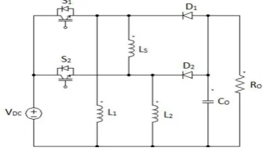
A. Circuit Configuration
The configuration of the frequency dependent boost converter is depicted in Fig 1. In this circuit two identical buck-boost converters operating in parallel. The source and the output capacitor Co are
shared between two converters. The interleaved inductor Ls is placed in parallel with two switches.
This element plays an important role in main plot of the soft switching manner of the converter. It discharges the intrinsic capacitances of the switches by creating a resonant circuit. Then, the switching could be done when the intrinsic anti parallel diodes of the switches conduct the negative half-cycle of this resonating current and the voltage on the switches is clamped at zero. . Two power MOSFETs, S1 and S2, are adopted high frequency switching
with the same switching frequency. The duty ratio D for each of the switches is identical and slightly greater than 0.5 to create overlapping intervals. It is assumed that the converters operate in the continuous current mode (CCM).
Fig 1: Configuration of frequency dependent boost
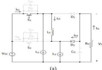
The equivalent circuit shown in Fig 2 is utilized to describe the procedure of the converter operation. To simplify the analysis, it is considered that the currents of inductors L1 and L2 and also the output
currents are constant, and modelled by a constant current source. Moreover, the output voltage is assumed to be almost fixed because of the large output capacitor C0. To describe how the ZVS is
achieved, the detailed models of the power MOSFETs are utilized. They consist of the intrinsic anti parallel diode and capacitance in parallel with an ideal switch. The operation procedure of the converter can be presented in eight modes depending on the different statuses of the switches. Because the two buck-boost converters are completely identical, all the circuit elements such as L1, L2, CS1, and CS2
have the same values. In all stages, the forward voltage drops on diodes D1 and D2, and switchesS1
and S2 are considered negligible. The equivalent
circuit of each mode is shown in Fig 3. The elements which are conduct are distinguished with the elements that are not. The theoretical waveforms related to each mode are demonstrated in figure 3.
Fig 2: Equivalent of frequency dependent boost converter
B. Modes of Operation
The operation of the converter can be explained in eight modes depending on the different statuses of the switches.
Mode 1: t0 < t < t1 : in this mode, it is considered
that the diode D2 freewheels the load current I0. So,
the diode D2 current is equal to IL1+IL2 and the
current IL1 passes through the inductor Ls reversely.
Mode I begin when the switch S1 is closed and D2
freewheeling current is decreasing to zero. Therefore, the voltage VDC +VO which was clamped on the
capacitor CS2 is imposed on the inductor LS by the
polarity depicted. Therefore, the inductor current IL2
increases linearly from -IL1 to IL2 as depicted in Fig 4.
Meanwhile, IS1 increases linearly simultaneous with
the ILS increment. As reaches zero, the current IL1
passes through the switch S1. When ILS rises up to IL2,
whole,VCS2 is considered to be constant and equal to
VDC +VO in this process. Fig 3(a) shows the
equivalent circuit diagram of this mode.
Mode 2: t1 < t < t2 : when the freewheeling current
of D2 reaches zero. Then, a resonant circuit is
formed between CS2 and ILS. This resonating current
discharges the capacitor CS2 which was clamped on
(VDC +VO) before entering this mode. After VCS2
decreases to zero, DS2 will be forward biased to
conduct the resumption of the resonant current cycle. Now, both of the resonant current and the inductor current through the interleaved inductor LS therefore,
ILS becomes a small bit larger than IL2, as shown in
Fig 4. Fig 3(b) shows the equivalent circuit diagram of this mode.
Mode 3: t2 < t < t3 : at the beginning of this mode,
DS2 whose voltage was xed at zero begins to conduct
a small current reversely through the switch S2 . This
current is the di erence between ILS and IL2 .
Therefore, the voltage across the switch S2 which is
the same as VCS2 becomes equal to zero as shown in
Fig 4. Thus, it is a great opportunity to apply the gate signal of the switch as VGS2 during this interval.
So, the switch S2 turns ON at the zero voltage.
Mode 4: t3 < t < t4 : at the beginning of this mode,
the gating signal of the switch S1 is removed and it is
turned OFF. Therefore, the intrinsic capacitor CS1 is
charged rapidly to VDC +VO by the sum of currents
IL2 and IL1. According to Fig 4, along with an
increase in the CS1 voltage, the current ILS begins to
decrease and reverses its direction towards to -IL1
because VCS1 is imposed on the inductor LS. By
applying the KVL to the end of this mode, the voltage of diode D1 becomes equal to zero. Thus, it
begins to freewheel the load current.
Due to the symmetry of the converter, Modes V to VIII could be summarized in similar scenarios for the switch S1.
(a)
(b)
(c)
(d)
Fig 3: Equivalent circuit diagrams of different operation modes. (a) Mode I. (b) Mode II. (c) Mode III. (d) Mode IV.
III.ANALYSISANDOPERATIONOF
INTERLEAVEDBOOSTCONVERTER
Interleaved boost converter connected with two shunted boost conversion units and an auxiliary inductor. The two identical boost converters working in parallel to produce the output voltage. The source and the output capacitor are shared between two converters.
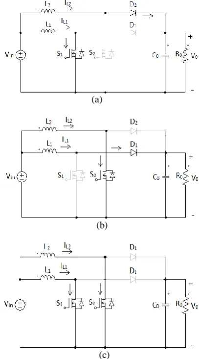
A. Circuit Configuration
The circuit configuration of parallel operated boost converter is depicted in Fig 5. It is composed of two identical boost converters working in parallel. The two power MOSFETs S1 and S2 are operated
with same switching frequency and same duty ratio. The interleaved boost converter consists of parallel connected switches S1 and S2 inductors L1 and L2,
diodes D1 and D2, Capacitor C and load resistor R
with common input source (Vin). The switches are controlled by phase shifted switching function known as interleaving operation.
Fig 5: Configuration of frequency dependent boost converter
B. Modes of Operation
Mode 1: In this mode, the switch S1 is on and S2 is
off . Diode D1 is reverse biased while diode D2 is
forward biased. The input supply energy to the inductor L1 resulting in rise of the inductor current
IL1 . At the same time, inductor L2 supplies energy to
the load resulting in decrease in inductor current IL2.
Mode 2: In this mode switch S2 is on and the switch
S1 is off . Diode D1 is forward biased while diode D2
is reverse biased. Inductor L1 discharging and
supplying energy to the load resulting in fall of the inductor current IL1.At the same time, the input
supplies energy to the inductor L2 resulting in
increase in inductor current IL2.
Mode 3: In this mode switch S2 and the switch S1 is
on. Both the diodes D1 and diode D2 are reverse
biased. This makes both inductors L1 and L2 charges
and resulting in increase of the inductor current IL1
and IL2.
(a)
(b)
(c)
Fig 6:Equivalent circuit diagrams of different operation modes. (a) Mode I (b) Mode II. (c) Mode III
IV.SIMULATIONMODELSANDRESULTS
The simulation of frequency dependent boost converter and interleaved boost converter is done in MATLAB R2014/Simulink and performance parameters of the two converters are verified.
A. Simulation and Results of Frequency Dependent Boost Converter
Table 1 describes the simulation parameters for the converter. Simulation of high frequency boost converter is carried out using an input of 20V, switching frequency fc of 133 kHz and 60 % duty
ratio.
1) Simulation Model of Frequency Dependent Boost Converter
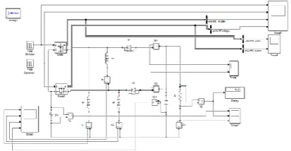
Fig 7 shows the Simulink model of frequency dependent boost converter. Simulation is performed with a 20V input DC source and a 25 ohm resistive load. The switching frequency has been considered 133 kHz. Two power MOSFETs S1 and S2, are
adopted for high frequency switching with the same switching frequency. The duty ratio D for each of the switches is identical and slightly greater than 0.5 to create overlapping intervals. The inductor LS
placed between two parallel converters is called the interleaved inductor. This element plays an important role in main plot of the soft switching manner of the converter. It is assumed that the converters operate in the continuous current mode (CCM).
Fig 7: Simulink model of Double deck buck-boost converter
2) Simulation Results of Frequency Dependent Boost Converter
Fig 8 and Fig 9 shows the switching pulse applied to the switches and volt-age across the switches. Stress across these switches is 23V. From the marked portions in the waveforms, it is clear that the switch voltage waveform create a zero-voltage condition for the switch to turn on. Thus zero voltage switching is achieved.
Fig 8: Simulation results of (a) Gate pulse of switch S1 (b) Voltage across switch S1 (c)Current through
switch S1.
Fig 9: Simulation results of (a) Gate pulse of switch S2 (b)Voltage across switch S2 (c)Current through
switch S2
Fig 10 shows the waveforms of input voltage, output voltage and output current. For an input voltage of 20 V, 133 kHz switching frequency and 0.6 duty ratio the output voltage is obtained is 41 V. That is the output voltage is boosted. The output voltage can be regulate by varying switching frequency instead of duty ratio.
Fig 10: Simulation results of (a) Input voltage (b)
Output voltage (c) output current
Current through the diodes and voltage across capacitor is shown in Fig 11. Ripple in the capacitor voltage C0 is 0.02 V.
Fig 11: Simulation results of (a) current through diode D1 (b) Current through diode D2 (c)Voltage
Current through the inductors L1, L2, and interleaved
inductor LS is shown in Fig 12. The ripple in the
inductor currents IL1 and IL2 is 0.29.
Fig 12: Simulation results of (a) Current through inductor L1 (b) Current through inductor L2 (c)
Current through inductor Ls
B. Simulation and Results of Interleaved Boost Converter
Table 2 describes the simulation parameters of the interleaved boost converter. Simulation of this converter is done with input voltage 20V, frequency 133 KHz and 60 % duty ratio.
Table II: Simulation parameter
3) Simulink Model of Interleaved Boost Converter
Simulink model of interleaved boost converter is shown in Fig 13. Simulation is performed with a 20V input DC source and a 25 ohm resistive load. The switching frequency has been considered 133 kHz. Two power MOSFETs S1 and S2, are adopted
for high frequency switching with the same switching frequency.
Fig 13: Simulink model of interleaved boost converter
1) Simulation Results of Interleaved Boost Converter
Fig 14 and Fig 15 shows the switching pulse applied to the switch S1 and S2. Voltage stress
Fig 14: Simulation results of (a) Gate pulse of Switch S1 (b) Voltage across switch S1
Fig 15: Simulation results (a) Gate pulse of switch S2 (b) Voltage across switch S2
Fig 16 shows the waveforms of input voltage, output voltage and output cur-rent. For an input voltage of 20 V, 133 kHz switching frequency and 0.6 duty ratio the output voltage is obtained is 48 V. That is the output voltage is boosted.
Fig 16: Simulation results of (a)Input voltage (b)Output voltage (c)output current
Fig 17 shows the current through the inductors and voltage across capacitor. The ripple in the inductor currents IL1 and IL2 is 0.5 . Ripple in the capacitor
voltage, C0 is 0.35 V.
Simulation results obtained verified the performance of the two converter. For an input voltage of 20 V, 133 kHz switching frequency and 60% duty ratio both the converters are simulated. In frequency dependent converter the value of ripple in the inductor currents and ripple in the output capacitor voltage is very low compared to parallel operated boost converter. The output voltage is regulated by varying the switching frequency instead of duty ratio. Zero voltage switching operation of the frequency dependent boost converter has been verified and the switches can be turned on at the zero voltage and it means that the switching losses can be decreased. Also voltage stress across switch is 23V in frequency dependent boost converter and 72V in parallel operated boost converter. That means in frequency dependent boost converter voltage stress is reduced compared to parallel operated boost converter.
V. COMPARATIVESTUDY
Voltage ripple across capacitor is 0.02 and 0.35 in frequency dependent boost converter and interleaved boost converter respectively. That means voltage ripple is negligible in frequency dependent boost converter. Voltage stress across switches is also reduced in frequency dependent boost converter compared to interleaved boost converter. From the comparative study it is clear that the frequency dependent boost converter is more improved converter than interleaved boost converter.
Table III: Comparison of frequency dependent boost converter and interleaved boost converter.
Frequency dependent boost converter have an output power of 90.2 W and 73.5 W for interleaved boost converter for an input power of 100 W. That is the efficiency of frequency dependent boost converter is increased by 18%.
Fig 18 shows the comparison of output voltage ripple of two converters. By increasing the frequency, the voltage ripple in frequency dependent boost converter is considerably reduced. So conclude that at high frequency, frequency dependent boost converter provides ripple free DC-DC conversion.
Fig 18: Frequency Vs Output voltage ripple
Fig 19 shows the variation of output voltage with duty ratio. Output voltage of interleaved boost converter increases with increasing the duty ratio. In frequency dependent boost converter output voltage is almost constant with increasing duty ratio. That is in frequency dependent boost converter the output voltage is independent of the duty ratio and depends only on frequency
Fig 19: Duty Ratio Vs Output voltage
VI.EXPERIMENTALRESULTS
To verify the theoretical and simulated results of frequency dependent boost converter 100W, 20 KHz prototype has been built. Table 4 shows the list of components used in the hardware implementation. Uses two power MOSFETs, power diodes, Inductors and capacitor with specifications obtained as in design. And also uses PIC controller and driver IC
Table IV: Components used for hardware
(a)
(b)
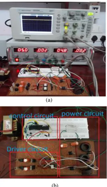
Fig. 20 (a) Experimental setup (b) Top view of the circuit
The Switching pulses of the switches are generated by using Pic16f877a processor. These are shown in Fig 21. Both the switches are adopted for high frequency switching with the same switching frequency 133 kHz. Both the switches are operated with 60 % duty ratio.
Fig 21: Pulses for switch S1 and switch S2
Fig 22 shows the output voltage waveform. For an input voltage of 5V, the obtained output voltage is 11V .The obtained output is compared with simulated output.
Fig 22: Output Voltage Waveform
VII. CONCLUSIONS
The performance parameters of the frequency dependent boost converter and interleaved boost DC-DC converter are analysed with various modes of operation and compared with simulated results using MATLAB/simulink. The output voltage ripple in the frequency dependent converter is 0.02 and 0.35 in interleaved boost converter. Ripple in current through inductor is 0.29 and 0.5 in frequency dependent boost converter and interleaved boost converter respectively. Voltage stress across switches is 23V in frequency dependent boost converter and 71V in interleaved boost converter. That is output voltage ripple and stress across switches in frequency dependent boost converter is reduced compared to interleaved boost converter. The two converters are compared by plotting duty ratio versus output voltage. The output voltage in frequency dependent boost converter is not greatly affected by varying duty ratio. The two converters are also compared by output voltage ripple for different frequencies. By increasing the frequency, the output voltage ripple in frequency dependent boost converter is greatly reduced compared to interleaved boost converter. By using frequency dependent boost converter, the system can has high voltage step up and smaller ripple at the output voltage and output current. The switching loss for this circuit also low. A prototype of 100W, 20 KHz is implemented using PIC16F877A controller. For an input voltage of 5V, output voltage of 11V is obtained and also zero voltage switching is achieved. The obtained output is compared with simulated output.
REFERENCES
[1] Erfan Maali and Behrooz Vahidi , "Double-Deck
Buck-Boost Converter With Soft Switching Operation", IEEE IEEE Transactions on Power Electronics, vol 31, No 6, June 2016.
[2] A.Thiyagarajan, S.G Praveen Kumar, and A.Nandini,
"Analysis and Comparison of Conventional and
Interleaved DC/DC boost converter", 2nd International Conference on Current Trends in Engineering and Technology, IC-CTET , July 2014.
[3] B. P. Divakar, K. W. E. Cheng, and D. Sutanto,
[4] Kui Jun Lee, B.-G. Park, R.-Y. Kim, and D.-S. Hyun, "Non-isolated ZVT two inductor boost converter with a single resonant inductor for high step-up applications", IEEE Transactions on Power Electronics, vol 27, No 4, pp 1966-1973, April 2012
[5] Martin Pavlovsky , G. Guidi , and A. Kawamura,
"Buck/boost dc-dc converter topology with soft switching in the whole operating region", IEEE Transactions on
Power Electronics, vol 29, No 2, pp 851-862, February
2014.
[6] C. Jingquan, D. Maksimovic, and R. W. Erickson,
"Analysis and design of a low-stress buck-boost converter in universal-input PFC applications", IEEE Trans-actions on Power Electronics , vol 21, No 2, pp 320-329, March 2006.
[7] E.-H. Kim and B.-H.Kwon, "Zero-voltage and zero-current
switching full bridge converter with secondary resonance", IEEE Transactions on Power Elecctronics , vol 57, No 3, pp 1017-1025, March 2010.
[8] Y. Wang, W. Liu, and L. Chen, "Resonance analysis and
soft switching design of isolated boost converter with coupled inductors for vehicle inverter application", IEEE Transactions on Power Electronics , vol 30, No 3, pp 1383-1392, March 2015.
[9] M. Pahlevaninezhad, P. Das, J. Drobnik, P. K. Jain, and A.
Bakhshai, "A ZVS in-terleaved boost AC/DC converter used in plug-in electric vehicles", IEEE Trans-actions on Power Electronics , vol 27, No 8, pp 3513-3529, August 2012
[10] Y. Gu and D. Zhang, "Interleaved boost converter with
ripple cancellation net-work", IEEE Transactions on Power