19 | P a g e
VHDL implementation of UART Module using FSM
Gaurav Verma
1, Vishal Rajput
2, Jashandeep Singh
31,2,3
Students, M.Tech VLSI Designing, ACSD, CDAC Mohali
ABSTRACT
With the technology advanced and the rising of SOC (System on Chip) concept resulting in designing of various modules in efficient manner to be embedded in smaller area, consuming less power and improvement in overall integration. UART which is an abbreviation for Universal Asynchronous Receiver Transmitter is a communication protocol majorly finds application in Microcontrollers and other standard data transfer interfaces. UART can be easily implemented by VHDL or Verilog can be demonstrated on a FPGA board for data transmission. This paper presents the basic implementation of UART module using FPGA and its implementation on Spartan 6.
Keywords :
Asynchronous, Microcontroller, FPGA
I.INTRODUCTION :
UART stands for Universal Asynchronous Receiver/Transmitter. UART is a circuit that controls the computer
interface so that the computer can exchange data with device. UART is a simple Half-duplex, Asynchronous,
Serial communication Protocol between two equivalent nodes generally between a processor and a peripheral.
The key functionality of UART involves the fact that receiver itself creates the clock by checking the baud rate
of the first bit of the frame. Serial transmission of digital information through a single wire or other medium is
less costly than parallel transmission through parallel wires. It is used for short distance, low cost data
transmission at the cost of low speed. The UART takes bytes of data and transmits individual bits in a sequential
fashion. The fundamental concept employed in UART is parallel to Serial data conversion at transmitter and
serial to parallel conversion at receiver end. Any node can initiate communication. Its parameter speed is
configurable which makes it universal. Each UART contains a shift register which is the fundamental method of
conversion between serial and parallel forms.
WORKING OF UART MODULE :
(a) TRANSMITTER
20 | P a g e
Figure 1
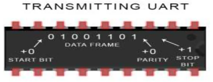
2. The transmitting UART adds the start bit, parity bit, and the stop bit(s) to the data received from the data bus
(Figure 2).
Figure 2
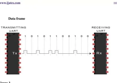
3. The transmitting UART sent the entire frame serially to the receiving UART. The receiving UART samples
21 | P a g e
Data frame
Figure 3
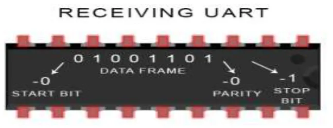
4- The receiving UART discards the start bit, parity bit, and stop bit from the data frame (Figure 4).
Figure 4
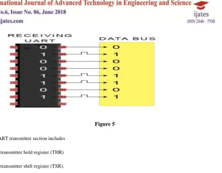
5. The receiving UART converts the serial data back into parallel and transfers it to the data bus on
22 | P a g e
Figure 5
The UART transmitter section includes
1. A transmitter hold register (THR)
2. A transmitter shift register (TSR).
When the UART is in the FIFO mode, THR is a 16-byte FIFO. Transmitter section control is a function of the
UART line control register (LCR). Based on the settings chosen in the LCR, the UART transmitter sends the
following to the receiving device:
1 START bit
5, 6, 7, or 8 data bits (as required)
1 PARITY bit (optional)
1 STOP bit
Software outputs a byte of data to the THR. The bits are immediately copied into an internal „shift‟-register. The
bits are shifted out, one-at-a-time, in sync with a clock-pulse.
(b) RECEIVER
23 | P a g e
Figure 6
2. The receiving UART converts the serial data back into parallel and transfers it to the data bus on the receiving
end (Figure 7).
Figure 7
The UART receiver section includes
1. A receiver shift register (RSR)
2. A receiver buffer register (RBR).
Receiver section control is a function of the UART line control register (LCR). The UART receiver accepts
following from transmitting device:
The receiving UART discards the start bit, parity bit, and stop bit from the data frame
• 1 START bit
24 | P a g e
• 1 PARITY bit (optional)
• 1 STOP bit
FINITE STATE MACHINE REPRESENTATION
It becomes quite easier for studying and implementation of a module with the use of FSMs. FSMs are symbolic
representation of a module with different states and their controlling signals for transitions.
TRANSMITTER STATE DIAGRAM
Figure 8
Figure 8 above shows the Finite State Machine representation of the transmitter section of UART Module
designed. Basically it has four states. Idle state is when the transmitter Reset is active and no action is being
performed. Then Load_Tx state allows the loading of data bits in register and addition of start and stop bits for
completion of frame. Then as UART is ready to transmit, Shift_Tx state is in operation where serial
transmission of bits takes place. Finally when all the bits in the frame are sent, the fourth state Stop_Tx is in
action where all the registers are cleared and Transmitter is sent back to idle state for next set of data
transmission.
Transmitter VHDL Code
library IEEE;
use IEEE.STD_LOGIC_1164.ALL;
use IEEE.STD_LOGIC_UNSIGNED.ALL;
entity uarttx1mar is
port
(
clk : in std_logic;
reset: in std_logic;
load : in std_logic;
frame: out std_logic_vector(5 downto 0);
25 | P a g e
end uarttx1mar;
architecture Behavioral of uarttx1mar is
signal tx_regdata : std_logic_vector(3 downto 0);
signal tx_reg : std_logic_vector(5 downto 0);
begin
process (reset, clk, tx_state)
begin
if (reset= '1') then
tx_regdata <= "1111";
tx_reg <= "111111";
tx_state <= tx_idle;
elsif rising_edge (clk) then
case tx_state is
when tx_idle =>
if load= '1' then
tx_regdata <= Din;
tx_state <= tx_load;
else tx_state <= tx_idle;
end if;
when tx_load =>
tx_state <= tx_shift;
tx_reg <= '1' & tx_regdata & '0'; // framing
when tx_shift =>
tx_reg <= '1' & tx_reg(tx_reg'high downto 1);
26 | P a g e
when tx_stop =>
tx_state <= tx_idle;
end case;
end if;
frame <= tx_reg;
end process;
end Behavioral;
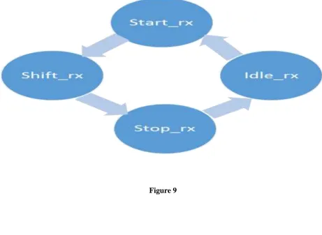
RECEIVER STATE DIAGRAM
27 | P a g e
As in the case of transmitter section, the corresponding receiver section is also designed using four states as
shown in figure 9. Here starting from Idle_Tx state where the receiver registers are all cleared. when the
receiver starts receiving the bits of frame and first start bit is received, Receiver moves to the Start_Rx start
where the start bit is sampled according to baud rate and required no of cycles to receive one bit is determined.
The registers are now ready for data reception and receiver is moved to Shift_Rx state where the bits are
simultaneously received and shifted in corresponding register. Finally at the completion of all bits of data frame
and stop bit the receiver is set to Stop_Rx state and here all the data is moved to output and receiver is finally set
to idle_rx state and makes the registers again clear for next set of reception.
Receiver VHDL Code
library IEEE;
use IEEE.STD_LOGIC_1164.ALL;
entity uartrx1mar is
port
(
clk :in std_logic;
reset:in std_logic;
ready : in std_logic;
rx_reg:inout std_logic_vector(5 downto 0);
Dout : out std_logic_vector (3 downto 0));
end uartrx1mar;
architecture Behavioral of uartrx1mar is
type rx_states is (rx_idle, rx_stop, rx_shift, rx_start);
signal rx_state : rx_states;
begin
process (reset,clk,rx_state)
28 | P a g e
if (reset='1') then
rx_reg <= (others =>'0');
Dout <= (others =>'0');
framerx <= (others =>'0');
rx_state <= rx_idle;
elsif rising_edge(clk) then
case rx_state is
when rx_idle =>
if (ready='1') then
framerx <= rx_reg;
rx_state <= rx_start;
else rx_state <= rx_idle;
end if;
when rx_start =>
if (framerx(5)='1') then
rx_state <= rx_shift;
end if;
when rx_shift =>
framerx <= '1' & framerx(framerx'high downto 1);
rx_state <= rx_stop;
when rx_stop =>
Dout<=framerx;
rx_state<= rx_idle;
end case;
29 | P a g e
end if;
end process;
end Behavioral;
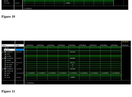
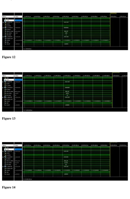
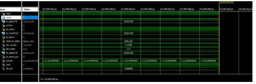
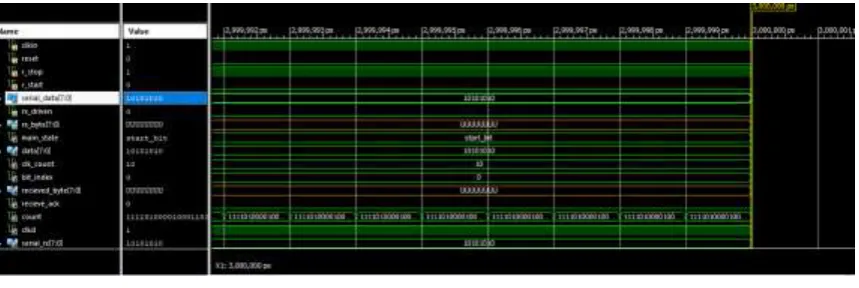
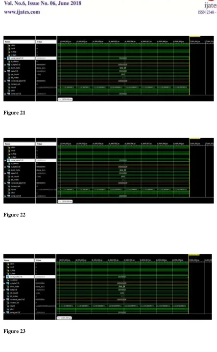
Output Waveforms :
The following figures from 10 to 26 show the transmission and reception of data bits through frame designed
with start and stop bits serially. These were obtained at simulation of VHDL Code separately by combining the
transmitter and receiver modules discussed above with a baud rate generator.
Figure 10
30 | P a g e
Figure 12
Figure 13
31 | P a g e
Figure 15
Figure 16
32 | P a g e
Figure 18
Figure 19
33 | P a g e
Figure 21
Figure 22
34 | P a g e
Figure 24
Figure 25
35 | P a g e
II.DISCUSSION:
UART module is implemented using VHDL and verified on FPGA SPARTON 6 kit. 8 bits of data were sent
and received successfully. Further detailed investigation can be done to verify the number of clock cycles
needed for receiving each bit. Sampling rates and baud rates can be varied for further variety of rates. Further
work can be in betterment including more number of states for improved data transmission.
REFERENCES
[1] FPGA implementation of Advanced UART Controller using VHDL, Arpita Tiwari, Ravi Mohran,
Divyanshu Rao, IMPACT : IJRET, Vol.2, Issue 8, August 2014, Pg 23-32
[2] VHDL Implementation of Universal Asynchronous Receiver Transmitter with Linear Feedback Shift
Register, Simarjeet Singh, Amardeep Kaur, IJARCSSE, Volume 7, Issue 5, May 2017
[3] Designing of UART using VHDL, Renuka Hingmire, Tamanna Jethwa, Aishwarya Askar, Sagar Mahajan,
Prashant Shende, ISSN, Volume-3, Issue-3, 2016
[4] A VHDL Implementation of UART Design with BIST Capability, Mohd Yamani Idris, Mushkuri Yaacob,
Zaidi Razak, University of Malaya, Malaysia, Malaysian Journal of Computer Science, Vol. 19 (1), 2006
[5] Fang Yi-yuan, Chen Xue-jun. "Design and Simulation of UART Serial Communication Module Based on
VHDL," Intelligent Systems and Applications (ISA), 2011 3rd International Workshop vol., no., pp.1-4, 28-29
May 2011.
[6] Naresh Patel, Vatsalkumar Patel and Vikaskumar Patel. “VHDL Implementation of UART with Status Register” 2012 International Conference on Communication Systems and Network Technologies (IEEE). [7] Hazim Kamal Ansari, Asad Suhail Farooqi. “Design Of High Speed Uart For Programming FPGA”
International Journal Of Engineering And Computer Science Volume1 Issue 1 Oct 2012