Design A New Stable And Low Power Bandgap
Reference Circuit Based On Fin-FET Device
Mohsen Jafari, Mohsen Imani
School of Electrical and Computer, Collage of Engineering, University of Tehran, Tehran, Iran;
ABSTRACT: This paper describes the design of a bandgap reference, implemented in 32 nm FinFET technology. The paper introduced new method for increasing stability of output voltage of bandgap circuit. In the proposed architecture extra feedback is used for setting the output voltage in fixed voltage. This feedback makesbandgap circuit more stable and speedy employing back gate biasing of the FinFET devices. This circuit generates a reference voltage of 300mV and has a variation about 0.041% versus temperature in TT corner. High gain OTA utilized in the feedback loop was designed by innovative bulk FinFET devices. FinFET OTA used in this work is very low power and high speed compared to conventional CMOS designs.It was tested with supply voltages between 0.7 and 0.9volt and between -40 ͦ C and +120 ͦ C. The variation of output voltage versus VDD variation is lower than 0.01% in TT corner. This circuit works in a current feedback mode, and it generates its own reference current, resulting in a stable operation. For resistor and diode connected transistor the technology elements were used instead of ideal components. The technology in use is 32 nm PTM.
Keywords: Bandgap reference, current feedback, FinFET, startup circuit, VDD variation 1 INTRODUCTION
A very popular element in each integrated circuit(IC) which is required for some application such as power management, data converters, voltage regulators and memories is a Bandgap Reference (BGR) circuit. There are a lot of research in designing low power digital and mixed signal electronic systems[1-3]. Its high stability against temperature and voltage variation is very favorable in every digital design. It could be designed by a couple of Bipolar Junction Transistors (BJT) which operate at different current density have different base-emitter voltage-each of them related to temperature. Voltage deference between the emitter of these pair of BJTs is not related to temperature or in the other words has zero temperature coefficients. For example for establishing a high precision ADC a critical part is the bandgap reference voltage. The basic of bandgap is related to two BJTs with different current density. Their difference makes it easier to cancel the negative temperature dependence of a simple PN junction and replace it with positive temperature dependence of a PTAT circuit which embodies some other elements a constant DC voltage is generated. This circuit can be designed such as the temperature dependence of the whole circuit was in propinquity to zero. Some innovative techniques are used to decrease this voltage so as can be scaled down with the technology scaling. One of them is the use of resistive subdivision technique with native transistors or diodes[4-6]. Some new techniques use a new technology for implement analog circuit such as FinFET based bandgap[7]. Some of other technique partially forward biases the PN junction of source bulk of PMOS transistors. Another example of 1V bandgap circuit uses the sub threshold region of transistors as a low voltage source or uses the differences between work functions material of gates for transistor with different doping concentration and types [8]. In order to implement lower than 1V bandgap circuit some others use the dynamic threshold MOSFET [8, 9]. However scaling down the reference voltage of the BGR results in lower noise resistance of the circuit some chopper stabilizing technique can be used to lower the noise of supply voltage and it should be considered as a tradeoff between supply voltage and noise resistance [10-12]. There more problems in order to design BGR in FinFET technology rather than conventional CMOS structures. It is due to difficulties of fabricating the diodes in thin SOI layer. Another disadvantage of the FinFET is that it is very hard to
implement resistors which have low area in the process employing only metal gate.A single ended Op-AMP is required to fix the drain voltage of MOS transistor. The structure of Op-Amp is fully discussed in this paper. Other details about each parts of the work consist of hand calculations about the circuit, transistor level and waves are also totally concerned and archived in this paper.
2
F
INFET
lithography and etch step in fabrication of the IC. Indeed underlap source/drain FinFETs show enhanced performance. The usage of this device is very attractive in now-a-days portable devices like cellular phones, wireless receivers and biomedical instruments. Several characteristics in design by FinFET should be conside3red to have process independent and high performance design [17-19].
Gate
Source
Drain
Figure 1. Lobster structure
3 PROPOSED ARCHITECTURE OF THE BANDGAP
This paper introduces an innovative topology in order to increase the accuracy and stability of the BGR. This topology can regulate the output voltage variation by changing the core current of the BGR and stabilize the output node’s voltage. The back gate of the PFET in the main body (M3) is biased by a feedback circuit which senses the output voltage variability due to PVT or even noise variation. The M5 sense the changes in the output voltage and amplify it as a common gate amplifier. This voltage is transferred by an active load as M4 to the back gate of the main PFET (M3) presented in the core branch. In other words, the more increase in the output voltage results in higher voltage in the drain of the sense transistor (M5). The more voltage biases the back gate of M3 increases the absolute value of the threshold voltage; hence the current of the output stage decreases and the output voltage fall down until it reaches the desired value. The ratio of the M4 to M5 should be chosen in such a way that they produce proper voltage of biasing the back gate of M3. The higher gain employed in this pair of transistor can sense even negligible change in the output voltage and regulate it in order to change the current of the M3. This can strongly increase
the accuracy of the output voltage accosting with PVT and noise changes. A BGR is created by addition of two voltages that one of them is negatively related to temperature while other has positive temperature coefficient. Proper multiplication weight is found by tuning the resulted voltage in different temperature. The difference between multiple VD of two diodes changes Proportional to Absolute Temperature (PTAT). The PTAT relationship is given by [20]
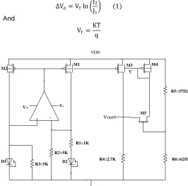
∆Vd = VTln
J2
J1
(1)
And
VT=KT q
V+
+ _
R3=5K R2=5K
R1=1K
D1 D2 R4=2.7K
M2 M1 M3
Vout
VDD
M4
R6=625Ω R5=375Ω
M5 Y
Figure 2. Sample circuit of a bandgap which used current mirror approach to decrease supply voltage coefficient
A new method of implementing a BGR is repressing as follow. Whole circuit consist of an independent supply voltage, 2 diode consist of FinFETswhich generate a voltage which decreases as temperature increase some resistor are used to improve the performance.Using a current mirror in top of the BJT will decrease the supply noise in output voltage. It also needs an op-amp whichcompleted the feedback loop. You could see a sample of bandgap circuit inFigure 2. The use of this FinFET could be possible because our sample circuit has diodes. If op-amp is ideal the voltage input op-amp nodes are equal and the voltage deference between diodes will drive the resistor-which are the real resistor technology. So if it is assumed that this resistor is ideal and follows the ohm’s law, it could be derived that:
R1 =∆VD Iss (2) And
Vref = VD.
R4 R2+ ∆VD.
R4
R1 (3)
And the output reference voltage could be set by weighting the Vbe voltages with resistors’ value.
4CASCODE
OP-AMP
The BGR needs a high input resistance OTA which is implemented in folded cascade to have low input common
Table 1. FinFET Parameter in 32nm technology
LG(nm) 32
Tox(A) 14
Tsi(nm) 8.6
VDD(V) 0.9
Channel Doping, NBODY (#/cm-3)
2×10¹⁶
Hfin (nm) 40
Vt0,nmos(V) 0.29
mode voltage.An op-amp is needed to implement the bandgap circuit and complete the feedback loop. In this paper a 1stage high swing folded cascode with DC gain about 1.29K in Typical-Typical corner and 27˚C was designed and was used in the bandgap circuit. Folded cascode is used because
of its wide common mode input voltage and low voltage of collector-emitter. The topology of the cascode OTA is depicted in
Figure 3.
M4
X3
VDD
M8
M12
M1 M2
M3
M7
M5 M6
M11
M13 M9
X3
MB1
MB2 MB3
M14
M15
M16
M17
M18 Vb
Vb
High PSRR Portion
Amplifier
V1 M10 V1
X2
X1
Figure 3. Topology of Folded Cascode OTA
OTA has maximum gain in SS corner and -40 ͦ C and minimum gain about 400 in SF corner and 120 ͦ C and in typical corner the gain is laid between them. The size of transistor for cascode OTA is tuned and finallythe total current is about 91µA for cascode which means this OTA uses only 82µW. This brings us a very low power and high performance architecture which can be used freely in the circuit as needed without worrying about its energy consumption. A voltage buffer is used in order to cancel the noise of reference voltage as illustrated in
Figure 4. This buffer should employ high gain OTA to achieve low output impedance and consequently low noise coupling on Vref. High gain in low power and low voltage is very hard and needs consideration of lots of design criteria. This allows the OTA to achieve high gain in lower than 1volte supply voltage. The differential structure of the buffer also tends to increase the offset in the reference voltage as symmetric or random noise[21].
Vref
A +
_
Figure 4. Buffer for FinFET based BGR
It’s also required that the current initiated from its zero state by a start-up circuit. A typical start-up circuit shown in
Figure 5may go to off mode quicker than the circuit’s voltages are stabilized. It is of particular concern when the size of the chip and number of the nodes are huge. Therefor some of the block may not start their functionality before the start-up circuit go off.
Ms2
Ms1
Ms3
X2
X1
Figure 5. Traditional Startup Circuit
5CIRCUIT ANALYSIS
In order to finding the temperature coefficient of the reference voltage the resistor assumed to be ideal and the temperature coefficient of diodes voltage, it could be gained that:
∂Vd = −0.6 T
Vd2= 0.6
V3= V2 R2= R3 ∆Vd = R0Ic2
Iout =VTln m R1
+Vbe 1 R2
∂Vref
∂T = ∂ ∂T R4
VTln m
R1 +
Vd 1
R2
And for minimum sensitivity to temperature in 300˚Kit should be zero.
∂Vref
∂T =
R4Kqln m
R1
−R4 R2
×0.6 T = 0
By considering the m=100 for BJTs and also R4=2.7K we could find:
R2
R1= 5
For writing the feedback formulathe Rout of M5 should be find, this equation are as:
5 1 / 4
D m
R g (5)
So the gain of feedback equal to:
5
f m D
A g R Af gm5/gm4 (6)
This equation shows that the gain of feedback is related to the gm ratio of M5 to M4. So with regulate this parameter the circuit canachieve to optimum gain.
6
SIMULATIONS AND FEATURES OF SELECTED BANDGAPThe gate control of the transistor in FinFET is much higher which reduce the short channel effects (SCE). The higher on-current of transistors and lower than 70mV/dec subthreshold slop in FinFET technology can utilize to have speedy device by lower power consumption.The usage of 32nm transistors makes proposed bandgap very compatible with digital parts of the integrated circuits (IC). This alluring characteristic is magnified through now-a-days ICs design with lower area and power for analog parts. In TT corner the variation of output voltage versus temperature between -40 ͦ C and 120 ͦ C is depicted in
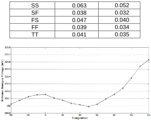
Figure 6. The variation in reference voltage isminimized in TT corner.The temperature dependence of output voltage in different process corners was found and archived in
Table 2. The temperature varied between -40 and 120 for bulk CMOS and FinFET devices respectively. The temperature dependency for long channel FinFET is lower than comparable CMOS transistors.
Table 2–Compare of variation in output voltage between -40 and 120 in all corners for bulk CMOS and FinFETdevices (%)
CORNER
Variation of output for
bulk CMOS (%)
Variation of output for
FinFET
SS 0.063 0.052
SF 0.038 0.032
FS 0.047 0.040
FF 0.039 0.034
TT 0.041 0.035
Figure 6. variation of reference voltage versus temperature in TT corner (0.041%)
Figure 7. Variation of output voltage versus VDD (0.01%)in TT corner
Final tuning was done to achieve the minimum variation in output voltage in all corners. This needs some deviation from the ratio of resistor was found by hand calculation. Then the supply voltage was swept between 10% of its value and the output voltage versus VDD was found as depicted inFigure 7.The variation of reference voltage under such variation is below 0.01%.Finally the circuit was tested under Monte-Carlo simulation to model random mismatch between components which are results of process variation. Applying the different value of VT was done by generating a Gaussian function for each of the parameters. Some data about Gaussian function is needed as follow:
η= the mean value of Threshold voltage σ2 = the variation of random data
very attractive and easy to fab. These numbers which demonstrate the density of Vref in different amplitudes were illustrated in Figure 8.
Figure 8. Distribution of Vref
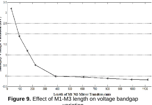
The most important factor affecting current symmetry of main BGR circuit and thus the output voltage is the Channel Length Modulation (CLM). The drain-source voltage of the M1-M3 pair transistor is dependent to the temperature severely. An amplifier is used in order to regulate this voltage and keep it in the same value for both transistors. Figure 9 shows the effect of M1-M3 transistors in BGR voltage.
Figure 9. Effect of M1-M3 length on voltage bandgap variation
the power Rejection of the circuit from supply voltage is demonstrated inFigure 10. With use of FinFET devices the circuits can achieve more PSRR than bulk CMOS.
Figure 10. Power supply Rejection
7 CONCLUSION
In this paper is introduced a new topology of bandgap voltage circuit. This architecture generate stable and regulate output voltage with using of extra feedback. This feedback makes circuit more stable against PVT variation and noise. Use of FinFET devices provide extra pin for controlling threshold voltage of this device bygiving the voltage to back gate of it. BGR is used from the back gate of output Stage as controller of output current.High gain OTA utilized in the feedback loop was designed by innovative bulk FinFET devices which are very low power and high speed compared to conventional CMOS designs . It was tested with supply voltages between 0.7 and 0.9 volt and between -40 ͦ C and +120 ͦ C. this circuit generates a reference voltage of 300mV with only 0.041% and 0.01% variation versus Temperature and VDD variation respectively. 32nm PTM technology is used for simulation
REFERENCES
[1] M. Jafari, M. Imani, M. Ansari, M. Fathipour, and N. Sehatbakhsh, "Design of an ultra-low power 32-bit adder operating at subthreshold voltages in 45-nm FinFET," in Design & Technology of Integrated Systems in Nanoscale Era (DTIS), 2013 8th International Conference on, 2013, pp. 167-168.
[2] M. Jafari, M. Imani, M. Fathipour, and N. Sehatbakhsh, "Bottom-up design of a high performance ultra-low power DFT utilizing multiple-V DD, multiple-Vth and gate sizing," in Design & Technology of Integrated Systems in Nanoscale Era (DTIS), 2013 8th International Conference on, 2013, pp. 178-179.
[3] M. Jafari, M. Imani, and M. Fathipour, "A 13 ENOB and 40MS/s Switched-Capacitor Sample & Hold Circuit Using a Two-Stage OTA with non-ideal components available in CMOS 0.18 µ technology."
[4] A. Lahiri and N. Agarwal, "Design of sub-1-V CMOS bandgap reference circuit using only one BJT," Analog Integrated Circuits and Signal Processing, vol. 71, pp. 359-369, 2012.
[6] P. B. Basyurt and D. Y. Aksin, "Untrimmed 6.2 ppm/° C bulk-isolated curvature-corrected bandgap voltage reference," Integration, the VLSI Journal, 2013.
[7] A. J. Annema, P. Veldhorst, G. Doornbos, and B. Nauta, "A sub-1V bandgap voltage reference in 32nm FinFET technology," in Solid-State Circuits Conference-Digest of Technical Papers, 2009. ISSCC 2009. IEEE International, 2009, pp. 332-333.
[8] C. J. B. Fayomi, G. I. Wirth, H. F. Achigui, and A. Matsuzawa, "Sub 1 V CMOS bandgap reference design techniques: a survey," Analog Integrated Circuits and Signal Processing, vol. 62, pp. 141-157, 2010.
[9] Y. Cao, W. De Cock, M. Steyaert, and P. Leroux, "A 4.5 MGy TID-Tolerant CMOS Bandgap Reference Circuit Using a Dynamic Base Leakage Compensation Technique," 2013.
[10]Y. Jiang and E. K. F. Lee, "A low voltage low 1/f noise CMOS bandgap reference," in Circuits and Systems, 2005. ISCAS 2005. IEEE International Symposium on, 2005, pp. 3877-3880.
[11]T. Tao, C. Fan, D. Chen, and J. Zhou, "A 1.8 V low noise threshold voltage reference generator with temperature and process calibration," in Solid-State and Integrated Circuit Technology (ICSICT), 2012 IEEE 11th International Conference on, 2012, pp. 1-3.
[12]M. Ansari, M. Imani, H. Aghababa, and B. Forouzandeh, "Estimation of joint probability density function of delay and leakage power with variable skewness," in Electronics, Computer and Computation (ICECCO), 2013 International Conference on, 2013, pp. 251-254.
[13]V. G. Ceekala, L. D. Lewicki, J. B. Wieser, D. Varadarajan, and J. Mohan, "A method for reducing the effects of random mismatches in CMOS bandgap references," in Solid-State Circuits Conference, 2002. Digest of Technical Papers. ISSCC. 2002 IEEE International, 2002, pp. 392-393.
[14]G. Knoblinger, F. Kuttner, A. Marshall, C. Russ, P. Haibach, P. Patruno, et al., "Design and evaluation of basic analog circuits in an emerging MuGFET technology," in SOI Conference, 2005. Proceedings. 2005 IEEE International, 2005, pp. 39-40.
[15]G. Crupi, D. M.-P. Schreurs, J.-P. Raskin, and A. Caddemi, "A comprehensive review on microwave FinFET modeling for progressing beyond the state of art," Solid-State Electronics, vol. 80, pp. 81-95, 2013.
[16]A. B. Sachid and C. Hu, "A little known benefit of FinFET over Planar MOSFET in highperformance circuits at advanced technology nodes," in SOI Conference (SOI), 2012 IEEE International, 2012, pp. 1-2.
[17]P. Mishra, A. Muttreja, and N. K. Jha, "FinFET Circuit Design," Nanoelectronic Circuit Design, pp. 23-54, 2011.
[18]G. Pei, J. Kedzierski, P. Oldiges, M. Ieong, and E. C. C. Kan, "FinFET design considerations based on 3-D simulation and analytical modeling," Electron Devices, IEEE Transactions on, vol. 49, pp. 1411-1419, 2002.
[19]B. Raj, A. Saxena, and S. Dasgupta, "Nanoscale FinFET Based SRAM Cell Design: Analysis of Performance Metric, Process Variation, Underlapped FinFET, and Temperature Effect," Circuits and Systems Magazine, IEEE, vol. 11, pp. 38-50, 2011.
[20]D. Hilbiber, "A new semiconductor voltage standard," in Solid-State Circuits Conference. Digest of Technical Papers. 1964 IEEE International, 1964, pp. 32-33.