Citation for published version:
Idígoras, J, Contreras-Bernal, L, Cave, JM, Courtier, NE, Barranco, Á, Borras, A, Sánchez-Valencia, JR, Anta, JA & Walker, AB 2018, 'The Role of Surface Recombination on the Performance of Perovskite Solar Cells: Effect of Morphology and Crystalline Phase of TiO2 Contact', Advanced Materials Interfaces, vol. 5, no. 21, 1801076. https://doi.org/10.1002/admi.201801076
DOI:
10.1002/admi.201801076
Publication date:
2018
Document Version
Peer reviewed version Link to publication
This is the peer reviewed version of the following article: Idígoras, J, Contreras-Bernal, L, Cave, JM, Courtier, NE, Barranco, Á, Borras, A, Sánchez-Valencia, JR, Anta, JA & Walker, AB 2018, 'The Role of Surface
Recombination on the Performance of Perovskite Solar Cells: Effect of Morphology and Crystalline Phase of TiO2 Contact' Advanced Materials Interfaces, vol. 5, no. 21, 1801076 which has been published in final form at: https://doi.org/10.1002/admi.201801076. This article may be used for non-commercial purposes in accordance with Wiley Terms and Conditions for Self-Archiving.
University of Bath
General rights
Copyright and moral rights for the publications made accessible in the public portal are retained by the authors and/or other copyright owners and it is a condition of accessing publications that users recognise and abide by the legal requirements associated with these rights. Take down policy
If you believe that this document breaches copyright please contact us providing details, and we will remove access to the work immediately and investigate your claim.
The Role of Surface Recombination on the
Performance of Perovskite Solar Cells: Effect of
Morphology and Crystalline Phase of TiO
2
Contact
Jesús Idígorasa,, Lidia Contreras-Bernala,, James M. Cavec, Nicola E. Courtierc, Ángel Barrancob, Ana Borrasb, J.R. Sánchez-Valenciab,*, Juan A. Antaa,*, Alison B. Walkerc,*
a Área de Química Física, Universidad Pablo de Olavide, Seville, E-41013, Spain.
b Instituto de Ciencia de Materiales de Sevilla (CSIC-Universidad de Sevilla), Seville, E-41092, Spain cDepartment of Physics, University of Bath, BA2 7AY, UK
ABSTRACT Herein, we report the preparation of one-dimensional TiO2 nanocolumnar films grown by plasma-enhanced chemical vapour deposition (PECVD) as the electron selective layer (ESL) for perovskite solar devices. Our analysis includes both the impact of the ESL architecture (one and three-dimensional morphologies) and the nanocrystalline phase (anatase and amorphous). For anatase structures, similar power conversion efficiencies were achieved using as ESL either the one-dimensional nanocolumns deposited by PECVD or the classical three-dimensional nanoparticle films prepared by spin-coating. However, lower power conversion efficiencies and different optoelectronic properties were found for perovskite devices based on amorphous one-dimensional films as ESL. The use of amorphous TiO2 as electron selective contact produces a bump in the reverse scan of the current-voltage curve as well as an additional electronic signal, detected by impedance spectroscopy (IS) measurements. The dependence of this additional signal on the optical excitation wavelength used in the IS experiments suggests that it stems from an interfacial process. Calculations using a drift-diffusion model which explicitly considers the selective contacts reproduces qualitatively the main features observed experimentally. From these calculations, it is inferred that the performance of the device with the amorphous contact is dominated by surface recombination, which induces a lower short-circuit photocurrent and more hysteresis, while not modifying significantly the open-circuit photovoltage. Our results demonstrate that for a solar cell in which the contact is working properly the open-circuit photovoltage is mainly determined by bulk recombination, whereas the introduction of a “bad contact” shifts the balance to surface recombination.
INTRODUCTION
Due to the excellent optoelectronic properties of hybrid organic-inorganic metal halide perovskite semiconductors,1–4 the photovoltaic field has undergone rapid progress over the last years due to the interest that employing these materials as active layers in solar cells has received from both the scientific and industrial community. Currently, the certified power conversion efficiency of perovskite solar cells (22.7%)5 is comparable to the photovoltaic performance of other thin-film photovoltaic technologies based on Si, CdTe and GaAs. This remarkable development has been possible due to the advances in terms of device engineering, material design and deposition/synthesis methods.6–9
In the most common PSC architecture, a mesoporous TiO2 nanoparticle film deposited onto a compact TiO2 layer and a Spiro-OMeTAD layer are employed as electron and hole selective materials, respectively. Under illumination, photogenerated electron-hole pairs in the perovskite layer separate into electrons and holes due to the high dielectric constant screening their mutual attraction, allowing migration and diffusion to drive the charge extraction to electron and hole selective layer (ESL, HSL). TiO2 is an especially suited material for electron injection due to its conduction band energy level. However, a large range of materials has also been employed as photoanodes or scaffolds (Al2O3, ZnO, ZrO2, Zn2SnO4).10–19 As in dye-sensitized solar cells20–23 or in photoelectrochemical applications,24,25 one-dimensional nanostructures (nanocolumns, nanorods, nanofibers, nanowires) have also been used as ESLs in PSCs. These vertically-aligned nanostructures have less grain boundaries than the classical three-dimensional nanoparticle films and consequently, as was theoretically demonstrated, show a faster electron transport and reduced charge recombination.26
Different wet chemical methods have been employed to synthesize these one-dimensional nanostructures: electrochemical anodization, electrodeposition or sol-gel synthesis. However, other techniques such as chemical vapour deposition, atomic layer deposition or vapour phase deposition give rise to structures with better electronic properties, lower impurities and higher crystallinity.27–32 These methods make it possible to synthesize one-dimensional nanostructures with a more homogeneous and reproducible character even in a large area, which is especially interesting for its industrial implementation.
The focus of this work is a fundamental study of the morphology of the TiO2/perovskite interface as regards its impact on the performance of the solar cell device. Its purpose is twofold. Firstly, we test the performance of the plasma-enhanced chemical vapor deposition (PECVD) technique to prepare TiO2 films to be used as ESL in perovskite solar devices. PECVD is a well-stablished technique in electronics and microelectronics, solar cells, mechanical engineering and optical industries for the fabrication of passive and active components. It provides an environmentally friendly (low-power and precursor consumption and solvent less approach) for the manufacturing in large scale with a finely control in the composition (including doping), microstructure and structure of thin films, coatings and interfaces in multilayer systems.28–34 Although this methodology has been traditionally applied in the deposition of compact layers, during the last years, our group has settled the conditions for the fabrication of tailored porous and nanostructured TiO2 thin films at low temperature (ranging from RT for amorphous to 250oC for anatase crystalline layers).34
Secondly, we aim to establish the effect of the nature of the ESL, in terms on morphology and crystallinity, on the photovoltaic performance. In particular, we investigate how bulk or
contact-induced recombination routes do influence the IV curve and the hysteretic behavior. The locus and nature of recombination in perovskite solar cells have been discussed thoroughly in the recent literature.35–38 The origin of hysteresis in the IV curve has also been object of intense debate.39–44 In this work we investigate the impact of the different nanostructures employed as ESL on the optoelectronic properties and the hysteresis. We have measured IV curves and run photoluminescence and impedance spectroscopy experiments. The latter are carried out with two excitation wavelengths, characterized by different optical penetration lengths in the perovskite layer, so that surface effects can be detected. In addition, drift-diffusion modelling, with explicit consideration of the ion/electron dynamics and the presence of the selective contacts, is used to generate IV curves.
In particular, we have found that anatase structures (both one and three-dimensional films) show exactly the same impedance response and similar power conversion efficiencies. In contrast, devices based on amorphous nanocolumnar films as ESL show an additional electronic process that appears to be related to interfacial processes and a more remarkable hysteresis. Drift-diffusion modelling indicates that a situation in which bulk recombination dominates explains the first set of experiments. However, the introduction of a more important contribution of the recombination at the TiO2/perovskite interface leads to lower values of the short-circuit photocurrent and more hysteresis. This prediction strongly suggest that this is the situation actually taking place when an amorphous TiO2 contact is used
EXPERIMENTAL SECTION
Perovskite solar cells were fabricated on FTO-coated glass (Pilkington–TEC15) patterned by laser etching. The substrates were cleaned using Hellmanex® solution and rinsed with deionized water and ethanol. Followed this they were ultrasonicated in 2-propanol and dried by using compressed air. Different methodologies were employed to prepare the different ETLs. For the standard configuration, a mesoporous layer of TiO2 was deposited on top of a TiO2 compact layer. The TiO2 blocking layer was deposited onto the substrates by spray pyrolysis at 450 °C, using a titanium diisopropoxide bis(acetylacetonate) solution (75% in 2-propanol, Sigma Aldrich) diluted in ethanol (1:3.5, v/v), with oxygen as carrier gas. The TiO2 compact layer was then kept at 450 °C for 30 min for the formation of anatase phase. Once the samples achieve room temperature, a TiO2 mesoporous layer was deposited by spin coating at 2000 rpm during 10 s using a TiO2 paste (Dyesol, 30NRD) diluted in ethanol (1:5, weight ratio). After drying at 100 °C for 10 min, the TiO2 mesoporous layer was heated at 500 °C for 30 min and later cooled to room temperature. The TiO2 nanocolumns deposition (anatase phase and amorphous) was carried out in a microwave electron cyclotron resonance (MW-ECR) PECVD reactor working in downstream configuration. The utilized plasma source was of the SLAN type operated with a power of 400 W with O2 as plasma gas at a pressure of 5 × 10⁻³ Torr. Titanium tetraisopropoxide, Ti(OC
3H7)4 (TTIP), was used as precursor bubbled to the plasma chamber by means of an O2 flow. We previously applied this
configuration for the deposition of TiO2 thin films as described in detail elsewhere.33,34 The
deposition at room temperature produces the formation of one-dimensional amorphous TiO2 nanocolumns, meanwhile heating of the substrates during deposition up to 300 ºC provides the crystallization to the anatase phase.34 The amorphous TiO
2 nanocolumnar samples were deposited onto a 40 nm compact TiO2 thin film fabricated by electron-beam evaporation using TiO2 pellets as target material. Deposition was carried out under a pressure of 5 10-4 mbar by flowing O2 into
the chamber to obtain a full oxidation to TiO2. These TiO2 layers deposited at room temperature were amorphous and the crystallization to the anatase phase was accomplished by annealing the samples in air at a temperature of 450ºC for 1 hour. This compact anatase films was deposited to provide a crystalline layer that facilitates the electron transport at the interface with the FTO.
For all the device configurations, a pure methylammonium (MAPbI3) layer was deposited as active
layer. The precursor solution was prepared to be deposited by spin coating under environmental humidity conditions (RH » 50%) using a methodology recently reported.45 According to this paper, the perovskite precursor solution was obtained from reacting DMF/DMSO (1:0.095 v/v) solution containing MAI and PbI2 (1:1 mol %) and DMF/DMSO (1:0.2 v/v) solution with a volume ratio of 1:0.45. The perovskite precursor solution (50 μL) was spin-coated in a one-step setup at 4000 rpm for 50 s. During this step, DMF is selectively washed with non-polar diethyl ether just before the white solid begins to crystallize in the substrate. Afterward the substrate was annealed at 100 °C for 3 min. Spiro-OMeTAD was subsequently deposited as hole selective layer (HSL) by dissolving 72.3 mg in 1 mL of chlorobenzene as well as 17.5 μL of a lithium bis (trifluoromethylsulphonyl)imide (LiTFSI) stock solution (520 mg of LiTFSI in 1mL of acetonitrile), and 28.8 μL of 4-tert-butylpyridine. The HTM solution was spin coated at 4000 rpm for 30 s. Finally, 60 nm of gold was deposited as a metallic contact by thermal evaporation under a vacuum level between 1·10-6 and 1·10-5 torr.
Characterization of Films and Devices
Current-voltage characteristics of the devices were obtained using a solar simulator (ABET-Sun2000) under 100mW/cm2 illumination with AM 1.5G filter. The light intensity was recorded
using a reference mono-crystalline silicon solar cell with temperature output (ORIEL, 91150). A metal mask was used to define an active area of 0.16 cm2. The current-voltage characteristics were determined by applying an external potential bias to the cell and measuring the photocurrent using an Autolab/PGSTAT302N potentiostat. The current-voltage characteristics were measured with a scan rate of 100 mV/s and a sweep delay of 20s.
The illumination for the different Impedance Spectroscopy (IS) measurements was provided by white, red (λ= 635 nm) and blue (λ= 465 nm) LEDs and over a wide range of DC light intensities. This allows for probing the devices at different positions of the Fermi level in the semiconductor and for different optical generation profiles. A response analyser module (PGSTAT302N/FRA2, Autolab) was utilized to measure the frequency response of the devices. To avoid voltage drop due to series resistance, IS measurements were performed at the open circuit potential. The Fermi level (related to the open-circuit voltage) was fixed by the DC illumination intensity. A 20mV perturbation in the 106-10-2 Hz range was utilized to obtain the spectra. To compensate for the different response under blue and red-light due to the different optical absorption, all parameters are monitored and plotted as a function of the open-circuit potential generated by each type of bias light. The NOVA 1.7 software was used to generate IS data. Z-view equivalent circuit modelling software (Scribner) was used to fit the spectra.
For the structural characterization, scanning electron microscope (SEM) images of the samples were performed using a Zeiss GeminiSEM-300 microscope working at 2 kV. X-ray diffractograms were recorded on a Rigaku diffractometer using CuKα source. The measurements were performed at grazing angle geometry. The samples were mounted without any further modification and the divergence slit were adjusted to the dimension of the films. The scan range of 10°- 60° was selected
with an acquisition time of 3 degree/min. A baseline correction was applied to the diffractograms to compensate for the noise arising from the substrate. For optical characterization, UV-Visible absorption spectra were recorded by using a Cary 100 UV-Vis spectrophotometer (Agilent) in the range of 400-850 nm. Steady state photoluminescence measurements were performed using a Hitachi, F-7000 Fluorescence spectrophotometer.
Drift-diffusion device modelling
The IV curves have been numerically simulated using a fully-coupled drift-diffusion model of charge carrier and halide ion dynamics in a perovskite solar cell. Our simulated device consists of a TiO2 electron selective layer, MAPbI3 absorber layer and spiro-OMeTAD hole selective layer. Electrons are constrained to the perovskite and TiO2 layers, while holes are constrained to the perovskite and spiro-OMeTAD layer. Ion vacancies are constrained to the perovskite. In one spatial dimension 𝑥, the behaviour of each species of particle over time 𝑡 is described by the drift-diffusion equation
𝜕𝑐 𝜕𝑡 = 𝐷
𝜕 𝜕𝑥'
𝑞𝑐 𝑘*𝑇
𝜕𝜙 𝜕𝑥 −
𝜕𝑐
𝜕𝑥. + 𝐺 − 𝑅,
where 𝑐 is the particle density, 𝐷 the diffusion coefficient, 𝑞 the elementary charge, 𝑘* the
Boltzmann constant, 𝑇 the temperature, 𝜙 the electric potential, 𝐺 net generation rate (sources) and 𝑅 the net recombination rate (sinks). The electric potential is found from the Poisson equation
𝜕3𝜙
𝜕𝑥3 = −
𝜌 𝜀 ,
Electrons and holes are generated within the perovskite with a Beer-Lambert profile given by
𝐺 = 𝐹89𝛼e<=>,
where 𝐹89 is the flux of photons incident on the device with energy above the bandgap and 𝛼 the
absorptivity of the perovskite. Recombination within the bulk of the perovskite is calculated using a combination of bimolecular (direct relaxation across the bandgap) and trap-assisted Shockley-Read-Hall (SRH) schemes, given by
𝐑𝐛𝐮𝐥𝐤 = 𝛃E𝐧𝐩 − 𝐧𝐢𝟐J + E𝐧𝐩 − 𝐧𝐢𝟐J
𝛕𝐧𝐩 + 𝛕𝐩𝐧
where 𝑛 and 𝑝 are the electron and hole densities, 𝜏O and 𝜏8 the SRH pseudolifetimes for electrons and holes. The intrinsic carrier density 𝑛P is defined as
𝑛P = 𝑔R𝑔Sexp '−
𝐸W 2𝑘*𝑇.
where 𝑔R and 𝑔S are the densities of states in the conduction and valence bands and 𝐸W the bandgap of the perovskite.
We also allow surface recombination, where a carrier in a transport layer recombines with an opposite carrier within the perovskite across the interface. We model this using a purely SRH mechanism, given by
𝑹𝑺 = 𝒏𝒑 − 𝒏𝒊𝟐 𝒑/𝒗𝒏 + 𝒏/𝒗𝒑,
where 𝑣O and 𝑣8 are the recombination velocities at the relevant interface. All parameters used in
the model are given in Table S1 in the Supporting Information. The only parameter changed between the two JV scans is the hole recombination velocity at the TiO2/MAPbI3 interface, which we increase from 10 m/s for Np-Anatase TiO2 to 1000 m/s for the Nc-amorphous TiO2.
We use a finite difference scheme for spatial discretisation, and integrate over time using the MATLAB ode15s (The MathWorks Inc., Natick, MA, USA) solver adapted for quadruple-precision arithmetic using the Advanpix Multiquadruple-precision Computing Toolbox. (Advanpix LLC, Yokohama, Japan). A full description of the method is detailed in Courtier et al.46 IV curves at 100 mV/s were simulated by varying the boundary conditions on the Poisson equation at this rate.
RESULTS AND DISCUSSION
To isolate the effect of the nanostructure and nanocrystalline phase of the different TiO2 films, a
fixed thickness of 200 nm was employed for all the different ETLs studied in this work. Figure 1A-C gathers cross-section SEM images of the three ETLs showing their corresponding characteristic microstructures, i.e., a homogeneous three-dimensional distribution of nanoparticles (Np-anatase) and vertical nanocolumns (Nc) for the PECVD thin films. In the case of the Nc-anatase, the columns are depicted for a feather-like morphology with sharp edges and rough surface. Nc-amorphous presents a domed form with the column diameter slightly thinner at the interface with the substrate. Figure S1 in the Supporting Information contains X-ray diffraction data of these TiO2 films.
Figure 1. Cross-section SEM views of the (A) Np-Anatase, (B) Nc-Anatase and (C) Nc-amorphous films deposited on silicon wafer. (D) Current-voltage characteristic in reverse scan under 1 sun – AM 1.5 illumination and (E) cyclic voltammetry using a white-LED as light source (10 mW·cm-2) for the different device configurations. A scan rate of 100 mV·s-1 with a poling of 20 s at 1.2V was employed in all three
cases.
On top of the TiO2 layer, a film of pure methylammonium lead iodide (MAPbI3) was deposited. Spiro-OmeTAD was used as hole selective layer in all cases. Figure S2 shows that the quality of the perovskite layer and their interface to HTM deposited on top is not affected by the morphology of the TiO2, and that there are no pinholes or voids that might compromise the stability of the device.47 Figure S3 also shows that the absorption properties of the perovskite films are basically unaffected by the morphology of the TiO2 layer. Hence, we can be fairly confident on the fact that only the electrical effect of the TiO2/perovskite interface is analysed for each configuration.
Figure 1D shows the best current-voltage characteristic obtained for the three device configurations measured under standard conditions (100 mW·cm-2 – AM 1.5 illumination). In particular, average efficiencies of 14.9%, 14.4% were obtained for Np-Anatase, Nc-Anatase devices, respectively (see also Figure S4 in the Supporting Information for full statistics details).
For Nc-Amorphous devices, the estimation of the efficiency is compromised by the appearance of a bump in the 0.6-0.8 voltage range (a lower efficiency is obtained in the forward scan, see Figure 1E) and therefore only an indicative value can be reported. No significant differences were found between the nanoparticle film (JSC: 19.8 mA·cm-2, VOC: 1020 mV, Fill Factor: 0.73) and the nanocolumnar film (JSC: 19.4 mA·cm-2, VOC: 1025 mV, Fill Factor: 0.73) as long as they have the same anatase TiO2 crystalline phase (see Figure S1 for the comparison of the XRD diagrams). In contrast, significant changes were observed when the nanocolumnar layer employed as ETL in perovskite devices is amorphous and does not show any crystalline phase (Figure S1, Figure S4). In spite of showing a similar VOC (1020 mV) to the ones obtained for Np-Anatase and Nc-Anatase devices (Table S1, Figure 1D), lower JSC values (15.9 mA·cm-2) were recorded and a prominent bump in the vicinity of the maximum power point is clearly visible. We note that the same scan rate of 100 mV/s is used for all devices. Similar behaviour has been found in both perovskite solar cells and dye-sensitized solar cells with strong hysteresis.36,37 In line with these results, as shown in Figure 1E, when the current-voltage characteristics were measured by cyclic voltammetry, Nc-Amorphous devices show strong hysteresis between reverse and forward scans in contrast to the Np-Anatase and Nc-Anatase devices, where the hysteresis is less significant. In particular, hysteresis indexes of 0.11, 0.13 and 0.61 were calculated for Np-anatase, Nc-Anatase and Np-Amorphous, respectively.
Figure 2. Steady state photoluminescence spectra of perovskite deposited on the top of the different ETLs. Al2O3 film was employed as reference. The excitation wavelength was 532 nm.
To investigate the influence of the different TiO2 films employed as ETLs on the charge extraction/separation efficiency, steady-state photoluminescence (PL) spectra of the perovskite films deposited on the top of each ETL were measured (Figure 2). In addition, a mesoporous Al2O3 nanoparticle film was also employed as reference due to its conduction band position and, consequently, its inability to accept electrons from the perovskite layer.10 In line with a previous work,48 using an excitation wavelength of 532 nm, PL peaks appear in the range of 785–815 nm with an emission maximum at 804 nm. The PL signal arises from radiative recombination processes within the perovskite material and therefore a faster electron injection from the perovskite film to the ETL results in a reduction of the PL signal. It is important to remember that the optical and structural properties of the perovskite film are not affected by the nature of the TiO2 layer and therefore by means of the PL experiment we probe the quality of the interface in
connection to the transfer of electrons towards the selective layer only.
The higher PL intensity was obtained when Al2O3 film was employed as ETL as a consequence of no electron extraction. Faster charge extraction was observed for the rest of ETLs, in the following
sequence: Np-Anatase > Nc-Anatase > Nc-Amorphous, with only a slight difference between the two anatase TiO2 layers. The worse charge extraction efficiency of Nc-Amorphous layers (Figure 2) could explain its lower JSC (Figure 1D, Table S1). However, in relative terms the photoluminescence difference between the three TiO2 layers is too small to have an impact on performance. Interfacial charge accumulation has been linked to hysteretic behaviour (Figure 1E).39,41
Figure 3. (A) Nyquist impedance spectra, (B) impedance frequency plot of the imaginary part (Z”) and (C) frequency-dependent apparent capacitance obtained for the different device configurations under open-circuit conditions and under white light illumination. The data were obtained for a photovoltage of 0.98 V at constant illumination.
To further analyze the impact of the different TiO2 layers employed as ETLs on the electronic dynamics that governs the photovoltaic performance, impedance spectroscopy measurements at open circuit were performed. In Figure 3, the impedance response in the form of Nyquist, frequency-dependent imaginary impedance Z” and capacitance plots are reported.
As shown Figure 3A, the impedance spectra obtained for the different devices were characterized by two signals (arcs). The signal that appears at low frequencies (LF) has been attributed to ionic motion and charge accumulation at the contacts.39,49 The high-frequency (HF) signal is likely to come mainly from losses due to bulk recombination in the perovskite layer,50–53 although as many authors have proposed, the recombination process also affects the LF signal.52,54,55 These two arcs (Figure 3A) will only be well-distinguished when the peak maxima on the impedance frequency plots (Figure 3B) lie separated enough in the frequency scale. In particular, for both Np-Anatase and Nc-Anatase the HF and LF peaks appear, under an applied potential closer to 1-sun VOC (» 980 mV), at 105 and 0.1Hz, respectively. In contrast, Nc-Amorphous devices show the HF and LF peaks at 104 and 10 Hz, respectively.
The frequency-dependent apparent capacitance for the different devices is shown in Figure 3C. Different polarization processes were attributed to each plateau.42,49,52,56 The HF component is determined by the dielectric polarization of the perovskite in the bulk, whereas the LF plateau has
been associated with the ETL/perovskite interface charge accumulation. It has been claimed that the hysteresis found in the current-voltage characteristics is associated with higher values of LF capacitance.39,42 However, in our case Nc-Amorphous devices show the most pronounced hysteretic behaviour (Figure 1E) in spite of showing lower LF capacitance values (»10-4 F) than in Np-Anatase and Nc-Anatase (»10-2 F). Furthermore, a new polarization process appears at mid frequencies for Nc-Amorphous devices. This new feature appears in the range of 103 – 104 Hz (Figure 3C), in the same range where the HF peak for Nc-Amorphous devices was found (Figure 3B). Thus, the presence of two time constants close in frequencies could explain the non-symmetric shape of the HF semicircle (Figure 3A) and the HF peak in the impedance frequency plots (Figure 3B) of Nc-Amorphous devices. A similar feature has previously been found for degraded perovskite devices57 as well as for cells with a non-optimized contact or when an insulating SiO2 scaffold is placed on top of the TiO2 selective layer.58
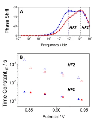
To better distinguish the time constants of the different processes found in the HF region of Nc-Amorphous devices, we have plotted the impedance phase shift versus frequency (Bode plot, Figure 4A). In contrast to Figure 3B, two peaks appear in the HF range (HF1» 104 Hz and HF2
»105 Hz), under an applied potential closer to 1-sun V
OC for Nc-Amorphous devices. Interestingly enough one of them (HF1) coincides in frequencies with the HF peak of Np-Anatase and Nc-Anatase devices. Considering the HF region only, Figure 4B shows the associated time constants (t) estimated as t = 1/2pf, where f is the frequency peak maximum directly extracted from the phase Bode plot (Figure 4A). As hinted above, the HF component can be associated with charge recombination processes and, consequently, the HF time constant could be understood as a
Figure 4. (A) Impedance frequency plot of phase shift, (B) HF time constants extracted as 1/2pf for the different device configurations under open-circuit conditions and under white light illumination. (C) HF resistance as extracted from fittings of the impedance spectra using [Rs-(R1CPE1)-(R2CPE2)] as equivalent circuit. Solid and open symbols correspond to the two time constants observed in the amorphous spectra in the HF region.
From the analysis of Figure 4, we can draw the following conclusions. Firstly, Np-Anatase and Nc-Anatase devices show the same basic recombination rate. Secondly, Nc-Amorphous devices exhibit two different kinetic processes in the high frequency region. As mentioned, the HF1 time constant, coincides remarkably well with the single HF time constant (10-6 – 10-5s) detected in the anatase films and attributed to charge recombination. In contrast, the HF2 time constant was found in the range of 10-5 – 10-4s with a different slope with respect to photopotential. Figure 4C shows the HF resistances as a function of the open-circuit photopotential extracted by fitting the impedance response to a simple [Rs-(R1CPE1)-(R2CPE2)] equivalent circuit. In particular, the HF1 recombination resistance is found to vary exponentially with the open-circuit potential as predicted by the following equation37,38
𝑅abR = cdefgh
di j <k
= 𝑅llexp c<mnio
pqj (1)
where Jrec is the recombination current, kB is the Boltzmann constant, T is the absolute temperature,
q is the elementary charge, R00 is the resistance at zero potential and b is the transfer or recombination parameter. As shown in Figure 4C, the HF1 resistance found for the different device configuration yields b parameter values around 0.56, very similar as the values obtained previously.38,60 The HF2 time resistance is also found to fit to Eq. (1) although with a different b
parameter value of 0.72. This suggest a different mechanism, possibly recombination, for Nc-Amorphous devices.
Figure 5. (A) Impedance frequency plot of phase shift and (B) HF time constants extracted as 1/2pf for Nc-Amorphous devices at open-circuit conditions and using red and blue light illumination
To cast light on the origin of HF time constants found for Nc-Amorphous devices, impedance spectroscopy was performed using two different illumination wavelengths. Considering the absorption spectra of perovskite devices (Figure S3) and the Beer-Lambert law, a different charge
generation profile inside perovskite layer will be produced using (l = 465 nm) blue and (l = 635 nm) red illuminations due to the different spatial penetration of the optical excitation wavelengths.61 In particular, a higher concentration of photogenerated charges is expected at the ETL/perovskite interface under blue illumination, whereas a more homogeneous charge generation profile would be created under red illumination. A similar methodology was previously employed to distinguish interfacial and bulk processes.57,62 Figure 5 shows the impedance phase shift versus frequency and time constant of the HF component extracted as t = 1/2pf for Nc-Amorphous devices using blue and red illuminations. Figure 5A brings to light the importance of where the charge has been photogenerated as shown by the different impedance responses obtained under the different optical excitation wavelengths. As shown in Figure 5B, the blue and red HF1 time constants coincide quite well in the studied voltage range. Similar results were found for Np-Anatase devices when impedance spectroscopy was performed under blue and red illuminations (Figure S5). However, the time constant HF2 does not only show a visible difference between the two time constants, but also a different slope. In particular, slower kinetics are observed when blue illumination was used as excitation wavelength. This behavior is consistent with the larger resistance observed in the Nyquist plot under blue illumination (Figure S6).
It is relevant to elucidate what is the physical origin of the additional HF2 time constant observed in the Nc-Amorphous devices and the strong hysteresis with a marked bump that it is observed in the IV curve. As noted above, the HF2 signal shows a different value when the impedance experiment is done at a situation where more carriers are photogenerated close to the front contact. All this evidence points to an interfacial process as the cause of the signal. The fact that amorphous contacts generate much less current at short-circuit suggests also that surface recombination may
As regards recombination, two main recombination mechanisms of photogenerated charges have been extensively discussed in the literature. On the one hand, a recombination process mediated via a trap-limited mechanism in the bulk of the perovskites.37,44,60,62 And, on the other hand, a surface-mediated recombination at the selective contacts.52,63,64 However, it is possible that the both recombination mechanisms could act together if the selective layer are characterized by a low charge extraction efficiency, as it is the case of Nc-amorphous layers studied here. As it was previously reported,62 the coincidence of the HF1 time constants obtained under blue and red illuminations, its time scale and the values of ideality factor (m ≈ 1.8) extracted from resistance versus potential plot (Figure 4C), indicate that this signal corresponds to recombination in the bulk of the perovskite layer via a trap-limited mechanism.35,60,62,65 In contrast, we attribute the different behaviour found for the HF2 time constants under blue and red illumination along with the ideality factor closer to 1 (m ≈ 1.4) to a surface-mediated recombination mechanism or, alternatively, to a slow transport process. In this respect, it is important to bear in mind that impedance time constants are not recombination “lifetimes”, especially for perovskite solar cells.47,48,50
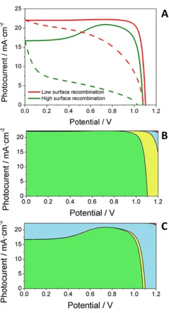
To confirm this interpretation, drift-diffusion modelling has been performed to simulate the IV curve for different relative values of surface versus bulk recombination. In these calculations the electron-hole dynamics, including transport and recombination, are coupled to the motion of iodide vacancies within the perovskite layer (see details above). In Figure 6 results for the IV curves for two cases, high and low surface recombination at the TiO2/perovskite interface, are shown.
The numerical simulation shows that a high value of the surface recombination rate does not only reduces the short-circuit photocurrent without affecting the VOC, but also induces more hysteresis in the voltage scan. This is perfectly in line with the experimental observations (Figure 1D, Figure
S4). Furthermore, the critical impact of the surface recombination term explains the appearance of the additional time constant in the impedance spectrum for the device with Nc-amorphous contact, as well its dependence on the excitation wavelength.
Figure 6. (A) Simulated IV curves for reverse (solid lines) and forward (dashed lines) when either high or low surface recombination rates at the TiO/perovskite interface are considered in the calculations. The rest of the parameters are
kept fixed. (B, C) Relative contributions to the total current: extracted current (green), bulk recombination (yellow), surface recombination at the TiO2 interface (blue) and surface recombination at the spiro interface (red).
In summary, considering the same behaviour obtained for the fastest recombination rate extracted from impedance spectroscopy (Figure 4B and Figure 5B) and the same VOC values (1020 mV) obtained from the current-voltage characteristics (Figure 1D and Figure S4) for all the different device configurations, trap-limited recombination in the bulk of the perovskites seems to be the main candidate to explain the open-circuit photopotential of perovskite devices, at least for anatase-base contacts. This is in line with recent reports with state-of-the art solar cells.44,60,62 However, an additional process appears for Nc-amorphous contacts, which also exhibit a bump in the current-voltage characteristics and strong hysteresis. We attribute this additional process and the IV curve shape to surface recombination at the TiO2/perovskite interface. It also important to state that at open-circuit, for Nc-amorphous contacts, bulk recombination still amounts to up to a third of the surface recombination, which explains the presence of the HF1 signal in the impedance spectrum in these devices.
CONCLUSIONS
In this work, we have analysed the impact of the structural and crystalline properties of different TiO2 films employed as ETL on the photovoltaic and optoelectronic behaviour of perovskite solar devices. In particular, we have investigated the effect of ETLs based on three-dimensional nanoparticle and one-dimensional nanocolumns films deposited by spin-coating method and plasma-enhanced chemical vapour deposition, respectively. Additionally, we have analysed the effect of the nanocrystalline phase of the ETL by comparing anatase and amorphous TiO2 nanocolumnar films.
Two main conclusions can be extracted from this work. On the one hand, the similar power conversion efficiency (»14.7%) and optoelectronic behaviour obtained for the both anatase TiO2 films (three and one-dimensional structure) employed as ETL bring to light the capacity to prepare well-performing one-dimensional photoanode by plasma-enhanced chemical vapour deposition technique, which is a very simple, reliable and industrially scalable and low-temperature deposition method. Secondly, regardless of the structural and crystalline properties of the different TiO2 films employed as ETL, all devices show the same open-circuit photopotential although quite different short-circuit photocurrent. This behaviour can be explained by two different charge recombination mechanisms present in devices based on amorphous nanocolumnar films as ETL. The results extracted from impedance analysis and drift-diffusion modelling reveal that the recombination mechanism that determines the open-circuit photopotential is governed by a process mediated via a trap-limited in the bulk of the perovskite. However, the second charge recombination mechanism found for amorphous nanocolumnar devices suggest that surface-mediated recombination at the ETL/perovskite interface determines the short-circuit photocurrent and the hysteresis.
AUTHOR INFORMATION Corresponding Author
E-mail: [email protected] E-mail: [email protected]
The manuscript was written through contributions of all authors. All authors have given approval to the final version of the manuscript. Jesús Idígoras and Lidia Contreras-Bernal have
contributed equally to this work.
ACKNOWLEDGMENTS
We thank Junta de Andalucía for financial support via grant FQM 1851 and FQM 2310. We thank Ministerio de Economía y Competitividad of Spain and Agencia Estatal de Investigación (AEI) and EU (FEDER) under grants MAT2013-47192-C3-3-R, 76892-C3-2-R, MAT2016-79866-R and Red de Excelencia “Emerging photovoltaic Technologies” for financial support. J.R. Sánchez-Valencia and A. Barranco acknowledge Marie Skłodowska-Curie Actions H2020-MSCA-IF-2014 PlasmaPerovSol grant (Project ID 661480). We also thank Servicio de Microscopía Electrónica (Universidad Pablo de Olavide). J.M. Cave and N.E. Courtier are supported by EPSRC funded studentships from the CDT in New and Sustainable Photovoltaics (reference EP/L01551X/1). A.B. Walker is supported by the Energy oriented Centre of Excellence (EoCoE), Horizon2020 grant research number 676629.
REFERENCES
(1) Xing, G.; Mathews, N.; Sun, S.; Lim, S. S.; Lam, Y. M.; Grätzel, M.; Mhaisalkar, S.; Sum, T. C. Long-Range Balanced Electron- and Hole-Transport Lengths in Organic-Inorganic CH3NH3PbI3. Science2013, 342 (6156), 344–347.
(2) Stranks, S. D.; Burlakov, V. M.; Leijtens, T.; Ball, J. M.; Goriely, A.; Snaith, H. J. Recombination Kinetics in Organic-Inorganic Perovskites: Excitons, Free Charge, and Subgap States. Phys. Rev. Appl.2014, 2 (3), 034007.
(3) Tress, W.; Marinova, N.; Inganäs, O.; Nazeeruddin, M. K.; Zakeeruddin, S. M.; Graetzel, M. Predicting the Open-Circuit Voltage of CH3NH3PbI3 Perovskite Solar Cells Using Electroluminescence and Photovoltaic Quantum Efficiency Spectra: The Role of Radiative and Non-Radiative Recombination. Adv. Energy Mater.2015, 5 (3), n/a-n/a.
(4) Manser, J. S.; Saidaminov, M. I.; Christians, J. A.; Bakr, O. M.; Kamat, P. V. Making and Breaking of Lead Halide Perovskites. Acc. Chem. Res.2016, 49 (2), 330–338.
(5) Yang, W. S.; Park, B.-W.; Jung, E. H.; Jeon, N. J.; Kim, Y. C.; Lee, D. U.; Shin, S. S.; Seo, J.; Kim, E. K.; Noh, J. H.; et al. Iodide Management in Formamidinium-Lead-Halide–Based Perovskite Layers for Efficient Solar Cells. Science2017, 356 (6345), 1376.
(6) Burschka, J.; Pellet, N.; Moon, S.-J.; Humphry-Baker, R.; Gao, P.; Nazeeruddin, M. K.; Grätzel, M. Sequential Deposition as a Route to High-Performance Perovskite-Sensitized Solar Cells. Nature2013, 499 (7458), 316–319.
(7) Zhou, H.; Chen, Q.; Li, G.; Luo, S.; Song, T.; Duan, H.-S.; Hong, Z.; You, J.; Liu, Y.; Yang, Y. Interface Engineering of Highly Efficient Perovskite Solar Cells. Science 2014, 345 (6196), 542–546.
(8) Jeon, N. J.; Noh, J. H.; Kim, Y. C.; Yang, W. S.; Ryu, S.; Seok, S. I. Solvent Engineering for High-Performance Inorganic–Organic Hybrid Perovskite Solar Cells. Nat Mater 2014, 13 (9), 897–903.
(9) Liu, M.; Johnston, M. B.; Snaith, H. J. Efficient Planar Heterojunction Perovskite Solar Cells by Vapour Deposition. Nature2013, 501 (7467), 395–398.
(10) Ball, J. M.; Lee, M. M.; Hey, A.; Snaith, H. Low-Temperature Processed Mesosuperstructured to Thin-Film Perovskite Solar Cells. Energy Environ. Sci.2013. (11) Son, D.-Y.; Im, J.-H.; Kim, H.-S.; Park, N.-G. 11% Efficient Perovskite Solar Cell Based
on ZnO Nanorods: An Effective Charge Collection System. J. Phys. Chem. C 2014, 118 (30), 16567–16573.
(12) Mahmud, M. A.; Elumalai, N. K.; Upama, M. B.; Wang, D.; Chan, K. H.; Wright, M.; Xu, C.; Haque, F.; Uddin, A. Low Temperature Processed ZnO Thin Film as Electron Transport Layer for Efficient Perovskite Solar Cells. Sol. Energy Mater. Sol. Cells 2017, 159, 251– 264.
(13) Kumar, M. H.; Yantara, N.; Dharani, S.; Graetzel, M.; Mhaisalkar, S.; Boix, P. P.; Mathews, N. Flexible, Low-Temperature, Solution Processed ZnO-Based Perovskite Solid State Solar Cells. Chem. Commun.2013, 49 (94), 11089–11091.
(14) Tseng, Z.-L.; Chiang, C.-H.; Wu, C.-G. Surface Engineering of ZnO Thin Film for High Efficiency Planar Perovskite Solar Cells. Sci. Rep.2015, 5, 13211.
(15) Bao, S.; Wu, J.; He, X.; Tu, Y.; Wang, S.; Huang, M.; Lan, Z. Mesoporous Zn2SnO4 as Effective Electron Transport Materials for High-Performance Perovskite Solar Cells. Electrochimica Acta2017.
(16) Batmunkh, M.; Macdonald, T. J.; Shearer, C. J.; Bat-Erdene, M.; Wang, Y.; Biggs, M. J.; Parkin, I. P.; Nann, T.; Shapter, J. G. Carbon Nanotubes in TiO2 Nanofiber Photoelectrodes for High-Performance Perovskite Solar Cells. Adv. Sci.2017, 4 (4), 1600504-n/a.
(17) Ramos, F. J.; Oliva-Ramirez, M.; Nazeeruddin, M. K.; Gratzel, M.; Gonzalez-Elipe, A. R.; Ahmad, S. Nanocolumnar 1-Dimensional TiO2 Photoanodes Deposited by PVD-OAD for Perovskite Solar Cell Fabrication. J. Mater. Chem. A2015, 3 (25), 13291–13298.
(18) Li, T. C.; Góes, M. S.; Fabregat-Santiago, F.; Bisquert, J.; Bueno, P. R.; Prasittichai, C.; Hupp, J. T.; Marks, T. J. Surface Passivation of Nanoporous TiO2 via Atomic Layer Deposition of ZrO2 for Solid-State Dye-Sensitized Solar Cell Applications. J. Phys. Chem. C2009, 113 (42), 18385–18390.
(19) Mejía Escobar, M. A.; Pathak, S.; Liu, J.; Snaith, H. J.; Jaramillo, F. ZrO2/TiO2 Electron Collection Layer for Efficient Meso-Superstructured Hybrid Perovskite Solar Cells. ACS Appl. Mater. Interfaces2017, 9 (3), 2342–2349.
(20) Gonzalez-Valls, I.; Lira-Cantu, M. Vertically-Aligned Nanostructures of ZnO for Excitonic Solar Cells: A Review. Energy Environ. Sci.2009, 2 (1), 19–34.
(21) González-García, L.; Idígoras, J.; González-Elipe, A. R.; Barranco, A.; Anta, J. A. Charge Collection Properties of Dye-Sensitized Solar Cells Based on 1-Dimensional TiO< Sub> 2 Porous Nanostructures and Ionic-Liquid Electrolytes. J. Photochem. Photobiol. Chem. 2012, 241, 58–66.
(22) Guillén, E.; Azaceta, E.; Vega-Poot, A.; Idígoras, J.; Echeberría, J.; Anta, J. A.; Tena-Zaera, R. ZnO/ZnO Core-Shell Nanowire Array Electrodes: Blocking of Recombination and Impressive Enhancement of Photovoltage in Dye-Sensitized Solar Cells. J. Phys. Chem. C 2013.
(23) Azaceta, E.; Idigoras, J.; Echeberria, J.; Zukal, A.; Kavan, L.; Miguel, O.; Grande, H.-J.; Anta, J. A.; Tena-Zaera, R. ZnO-Ionic Liquid Hybrid Films: Electrochemical Synthesis and Application in Dye-Sensitized Solar Cells. J. Mater. Chem. A2013, 1 (35), 10173–10183. (24) Idígoras, J.; Anta, J. A.; Berger, T. Charge-Transfer Reductive in Situ Doping of
Mesoporous TiO2 Photoelectrodes: Impact of Electrolyte Composition and Film Morphology. J. Phys. Chem. C2016, 120 (49), 27882–27894.
(25) Meekins, B. H.; Kamat, P. V. Got TiO2 Nanotubes? Lithium Ion Intercalation Can Boost Their Photoelectrochemical Performance. ACS Nano2009, 3 (11), 3437–3446.
(26) Gonzalez-Vazquez, J.; Morales-Flórez, V.; Anta, J. A. How Important Is Working with an Ordered Electrode to Improve the Charge Collection Efficiency in Nanostructured Solar Cells? J. Phys. Chem. Lett.2012, 3 (3), 386–393.
(27) Biyikli, N.; Haider, A. Atomic Layer Deposition: An Enabling Technology for the Growth of Functional Nanoscale Semiconductors. Semicond. Sci. Technol.2017, 32 (9), 093002. (28) Barranco, A.; Borras, A.; Gonzalez-Elipe, A. R.; Palmero, A. Perspectives on Oblique
Angle Deposition of Thin Films: From Fundamentals to Devices. Prog. Mater. Sci.2016, 76, 59–153.
(29) Choy, K. L. Chemical Vapour Deposition of Coatings. Prog. Mater. Sci.2003, 48 (2), 57– 170.
(30) Martinu, L.; Poitras, D. Plasma Deposition of Optical Films and Coatings: A Review. J. Vac. Sci. Technol. Vac. Surf. Films2000, 18 (6), 2619–2645.
(31) Ostrikov, K. (Ken); Cvelbar, U.; Murphy, A. B. Plasma Nanoscience: Setting Directions, Tackling Grand Challenges. J. Phys. Appl. Phys.2011, 44 (17), 174001.
(32) Roca i Cabarrocas, P. Plasma Enhanced Chemical Vapor Deposition of Silicon Thin Films for Large Area Electronics. Curr. Opin. Solid State Mater. Sci. 2002, 6 (5), 439–444. (33) Borrás, A.; Sánchez-Valencia, J. R.; Garrido-Molinero, J.; Barranco, A.; González-Elipe,
A. R. Porosity and Microstructure of Plasma Deposited TiO2 Thin Films. Microporous Mesoporous Mater.2009, 118 (1), 314–324.
(34) Borras, A.; Sanchez-Valencia, J. R.; Widmer, R.; Rico, V. J.; Justo, A.; Gonzalez-Elipe, A. R. Growth of Crystalline TiO2 by Plasma Enhanced Chemical Vapor Deposition. Cryst. Growth Des.2009, 9 (6), 2868–2876.
(35) Leong, W. L.; Ooi, Z.-E.; Sabba, D.; Yi, C.; Zakeeruddin, S. M.; Graetzel, M.; Gordon, J. M.; Katz, E. A.; Mathews, N. Identifying Fundamental Limitations in Halide Perovskite Solar Cells. Adv. Mater.2016, 28 (12), 2439–2445.
(36) Bi, D.; Tress, W.; Dar, M. I.; Gao, P.; Luo, J.; Renevier, C.; Schenk, K.; Abate, A.; Giordano, F.; Baena, J.-P. C.; et al. Efficient Luminescent Solar Cells Based on Tailored Mixed-Cation Perovskites. Sci. Adv.2016, 2 (1), e1501170.
(37) Correa-Baena, J.-P.; Turren-Cruz, S.-H.; Tress, W.; Hagfeldt, A.; Aranda, C.; Shooshtari, L.; Bisquert, J.; Guerrero, A. Changes from Bulk to Surface Recombination Mechanisms between Pristine and Cycled Perovskite Solar Cells. ACS Energy Lett.2017, 2 (3), 681–688. (38) Contreras-Bernal, L.; Salado, M.; Todinova, A.; Calio, L.; Ahmad, S.; Idígoras, J.; Anta, J. A. Origin and Whereabouts of Recombination in Perovskite Solar Cells. J. Phys. Chem. C 2017, 121 (18), 9705–9713.
(39) Contreras, L.; Idigoras, J.; Todinova, A.; Salado, M.; Kazim, S.; Ahmad, S.; Anta, J. A. Specific Cation Interactions as the Cause of Slow Dynamics and Hysteresis in Dye and Perovskite Solar Cells: A Small-Perturbation Study. Phys. Chem. Chem. Phys. 2016, 18 (45), 31033–31042.
(40) Ravishankar, S.; Almora, O.; Echeverría-Arrondo, C.; Ghahremanirad, E.; Aranda, C.; Guerrero, A.; Fabregat-Santiago, F.; Zaban, A.; Garcia-Belmonte, G.; Bisquert, J. Surface Polarization Model for the Dynamic Hysteresis of Perovskite Solar Cells. J. Phys. Chem. Lett.2017, 8 (5), 915–921.
(41) Zou, Y.; Holmes, R. J. Temperature-Dependent Bias Poling and Hysteresis in Planar Organo-Metal Halide Perovskite Photovoltaic Cells. Adv. Energy Mater.2016, 6 (7). (42) Kim, H.-S.; Jang, I.-H.; Ahn, N.; Choi, M.; Guerrero, A.; Bisquert, J.; Park, N.-G. Control
of I–V Hysteresis in CH3NH3PbI3 Perovskite Solar Cell. J. Phys. Chem. Lett.2015, 6 (22), 4633–4639.
(43) Richardson, G.; O’Kane, S. E. J.; Niemann, R. G.; Peltola, T. A.; Foster, J. M.; Cameron, P. J.; Walker, A. B. Can Slow-Moving Ions Explain Hysteresis in the Current–Voltage Curves of Perovskite Solar Cells? Energy Environ. Sci.2016.
(44) Ravishankar, S.; Gharibzadeh, S.; Roldán-Carmona, C.; Grancini, G.; Lee, Y.; Ralaiarisoa, M.; Asiri, A. M.; Koch, N.; Bisquert, J.; Nazeeruddin, M. K. Influence of Charge Transport Layers on Open-Circuit Voltage and Hysteresis in Perovskite Solar Cells. Joule2018, 2 (4), 788–798.
(45) Aranda, C.; Cristobal, C.; Shooshtari, L.; Li, C.; Huettner, S.; Guerrero, A. Formation Criteria of High Efficiency Perovskite Solar Cells under Ambient Conditions. Sustain. Energy Fuels2017, 1 (3), 540–547.
(46) Courtier, N. E.; Richardson, G.; Foster, J. M. A Fast and Robust Numerical Scheme for Solving Models of Charge Carrier Transport and Ion Vacancy Motion in Perovskite Solar Cells. ArXiv180105737 Phys.2018.
(47) Abate, A.; Paek, S.; Giordano, F.; Correa-Baena, J.-P.; Saliba, M.; Gao, P.; Matsui, T.; Ko, J.; Zakeeruddin, S. M.; Dahmen, K. H.; et al. Silolothiophene-Linked Triphenylamines as Stable Hole Transporting Materials for High Efficiency Perovskite Solar Cells. Energy Environ. Sci.2015, 8 (10), 2946–2953.
(48) Salado, M.; Idigoras, J.; Calio, L.; Kazim, S.; Nazeeruddin, M. K.; Anta, J. A.; Ahmad, S. Interface Play between Perovskite and Hole Selective Layer on the Performance and Stability of Perovskite Solar Cells. ACS Appl. Mater. Interfaces2016, 8 (50), 34414–34421. (49) Zarazua, I.; Bisquert, J.; Garcia-Belmonte, G. Light-Induced Space-Charge Accumulation Zone as Photovoltaic Mechanism in Perovskite Solar Cells. J. Phys. Chem. Lett.2016, 7 (3), 525–528.
(50) Guillén, E.; Ramos, F. J.; Anta, J. A.; Ahmad, S. Elucidating Transport-Recombination Mechanisms in Perovskite Solar Cells by Small-Perturbation Techniques. J. Phys. Chem. C 2014, 118 (40), 22913–22922.
(51) Todinova, A.; Idígoras, J.; Salado, M.; Kazim, S.; Anta, J. A. Universal Features of Electron Dynamics in Solar Cells with TiO2 Contact: From Dye Solar Cells to Perovskite Solar Cells. J. Phys. Chem. Lett.2015, 6 (19), 3923–3930.
(52) Guerrero, A.; Garcia-Belmonte, G.; Mora-Sero, I.; Bisquert, J.; Kang, Y. S.; Jacobsson, T. J.; Correa-Baena, J.-P.; Hagfeldt, A. Properties of Contact and Bulk Impedances in Hybrid Lead Halide Perovskite Solar Cells Including Inductive Loop Elements. J. Phys. Chem. C 2016, 120 (15), 8023–8032.
(53) Dualeh, A.; Moehl, T.; Tétreault, N.; Teuscher, J.; Gao, P.; Nazeeruddin, M. K.; Grätzel, M. Impedance Spectroscopic Analysis of Lead Iodide Perovskite-Sensitized Solid-State Solar Cells. ACS Nano2014, 8 (1), 362–373.
(54) Pockett, A.; Eperon, G. E.; Sakai, N.; Snaith, H. J.; Peter, L. M.; Cameron, P. J. Microseconds, Milliseconds and Seconds: Deconvoluting the Dynamic Behaviour of Planar Perovskite Solar Cells. Phys. Chem. Chem. Phys.2017, 19 (8), 5959–5970.
(55) Zarazua, I.; Han, G.; Boix, P. P.; Mhaisalkar, S.; Fabregat-Santiago, F.; Mora-Seró, I.; Bisquert, J.; Garcia-Belmonte, G. Surface Recombination and Collection Efficiency in Perovskite Solar Cells from Impedance Analysis. J. Phys. Chem. Lett.2016, 7 (24), 5105– 5113.
(56) Bag, M.; Renna, L. A.; Adhikari, R. Y.; Karak, S.; Liu, F.; Lahti, P. M.; Russell, T. P.; Tuominen, M. T.; Venkataraman, D. Kinetics of Ion Transport in Perovskite Active Layers and Its Implications for Active Layer Stability. J. Am. Chem. Soc.2015, 137 (40), 13130– 13137.
(57) Salado, M.; Contreras-Bernal, L.; Calio, L.; Todinova, A.; Lopez-Santos, C.; Ahmad, S.; Borras, A.; Idigoras, J.; Anta, J. A. Impact of Moisture on Efficiency-Determining Electronic Processes in Perovskite Solar Cells. J. Mater. Chem. A 2017, 5 (22), 10917– 10927.
(58) Anaya, M.; Zhang, W.; Hames, B. C.; Li, Y.; Fabregat-Santiago, F.; Calvo, M. E.; Snaith, H. J.; Miguez, H.; Mora-Sero, I. Electron Injection and Scaffold Effects in Perovskite Solar Cells. J Mater Chem C2017, 5 (3), 634–644.
(59) Pydzińska, K.; Karolczak, J.; Kosta, I.; Tena-Zaera, R.; Todinova, A.; Idígoras, J.; Anta, J. A.; Ziółek, M. Determination of Interfacial Charge-Transfer Rate Constants in Perovskite Solar Cells. ChemSusChem2016, 9 (13), 1647–1659.
(60) Tress, W.; Yavari, M.; Domanski, K.; Yadav, P.; Niesen, B.; Correa Baena, J. P.; Hagfeldt, A.; Graetzel, M. Interpretation and Evolution of Open-Circuit Voltage, Recombination, Ideality Factor and Subgap Defect States during Reversible Light-Soaking and Irreversible Degradation of Perovskite Solar Cells. Energy Env. Sci2017.
(61) Yang, Y.; Yang, M.; Moore, D. T.; Yan, Y.; Miller, E. M.; Zhu, K.; Beard, M. C. Top and Bottom Surfaces Limit Carrier Lifetime in Lead Iodide Perovskite Films. Nat. Energy2017, 2, 16207.
(62) Contreras Bernal, L.; Salado, M.; Todinova, A.; Calio, L.; Ahmad, S.; Idígoras, J.; Anta, J. A. Origin and Whereabouts of Recombination in Perovskite Solar Cells. J. Phys. Chem. C 2017, 10.1021/acs.jpcc.7b01206.
(63) Nie, W.; Tsai, H.; Asadpour, R.; Blancon, J.-C.; Neukirch, A. J.; Gupta, G.; Crochet, J. J.; Chhowalla, M.; Tretiak, S.; Alam, M. A.; et al. High-Efficiency Solution-Processed Perovskite Solar Cells with Millimeter-Scale Grains. Science2015, 347 (6221), 522.
(64) Li, D.; Bretschneider, S. A.; Bergmann, V. W.; Hermes, I. M.; Mars, J.; Klasen, A.; Lu, H.; Tremel, W.; Mezger, M.; Butt, H.-J.; et al. Humidity-Induced Grain Boundaries in MAPbI3 Perovskite Films. J. Phys. Chem. C2016, 120 (12), 6363–6368.
(65) Tress, W. Perovskite Solar Cells on the Way to Their Radiative Efficiency Limit – Insights Into a Success Story of High Open-Circuit Voltage and Low Recombination. Adv. Energy Mater.2017, 7 (14), 1602358-n/a.