HAL Id: insu-01344719
https://hal-insu.archives-ouvertes.fr/insu-01344719
Submitted on 1 Sep 2016
HAL is a multi-disciplinary open access archive for the deposit and dissemination of sci-entific research documents, whether they are pub-lished or not. The documents may come from teaching and research institutions in France or abroad, or from public or private research centers.
L’archive ouverte pluridisciplinaire HAL, est destinée au dépôt et à la diffusion de documents scientifiques de niveau recherche, publiés ou non, émanant des établissements d’enseignement et de recherche français ou étrangers, des laboratoires publics ou privés.
MODULAR APPROACH FOR AN ASIC
INTEGRATION OF ELECTRICAL DRIVE
CONTROLS �� � ��
Youssef Kebbati
To cite this version:
Youssef Kebbati. MODULAR APPROACH FOR AN ASIC INTEGRATION OF ELECTRICAL DRIVE CONTROLS �� � . �� IJE Transactions, 2011, 24 (2). �insu-01344719�
IJE Transactions B: Applications Vol. 24, No. 2, July 2011 -
107
MODULAR APPROACH FOR AN ASIC INTEGRATION OF
ELECTRICAL DRIVE CONTROLS
Y. Kebbati*
Universiy of Orléans, OSUC Observatoire des Sciences de l’Univers en Région Centre Campus Géosciences 1 A rue de la Férolerie 45071 ORLEANS CEDEX (France)
*Corresponding Author
(Received: November 12, 2009– Accepted in Revised Form:June 22, 2011)
Abstract VLSI circuits design allows today to consider new modes of implementation for electrical controls. However, design techniques require an adaptation effort that few designers, too accustomed to the software approach, provide. The authors of this article propose to develop a methodology to guide the electrical designers towards optimal performances of control algorithms implementation. Thus, they were based on two concepts: modular design and algorithm architecture adequation. An exemple of DTC control implemented in an ASIC circuit is presented and the results of the integration performances valid our methodology.
Keywords ASIC, FPGA, Electrical System Control, Modular Design, Algorithm Architecture Adequation,
Direct Torque Control.
ﮑﭼ
ﻴ
ﻩﺪ
،ﻩﺯﻭﺮﻣﺍ ﺣﺍﺮﻃ ﻲ ﺎﻫﺭﺍﺪﻣ ﻱ VLSI ﺘﻟﺎﺣ ﻲ ﺪﺟ ﻳ
ﺍﺮﺑﺪ
ﻱ
ﺯﺍﺪﻧﺍﻩﺍﺭ
ﻱ
ﺎﻫﻝﺮﺘﻨﮐ
ﻱ ﺮﺘﮑﻟﺍ ﻳ ﮑ ﻲ ﺖﺳﺍ
.
ﺵﻭﺭ،ﻝﺎﺣﺮﻫﻪﺑ
ﺎﻫ ﻱ ﺣﺍﺮﻃ ﻲ
ﻼﺗﻪﺑ
ﺷ ﻲ ﻘﺑﺎﻄﺗ ﻲ ﻧﻴ
ﺩﺍﺪﻌﺗﻪﮐﺩﺭﺍﺩ ﺯﺎ
ﻱ
ﺎﻫﺵﻭﺭﻪﺑﻪﺘﻓﺮﮔﻮﺧﻥﺎﺣﺍﺮﻃﺯﺍ
ﻱ
ﺭﺍﺰﻓﺍ ﻡﺮﻧ
ﻱ
ﺍﺍﺭ ﻥﺁ،
ﻳ
ﻣﺩﺎﺠ
ﻲ ﻨﻨﮐ ﺪ
.
ﻮﻧ ﻳ
ﺍ ﻥﺎﮔﺪﻨﺴ
ﻳ
ﻪﻌﺳﻮﺗ ،ﻪﻟﺎﻘﻣ ﻦ
ﺷﻭﺭ ﻲ ﺍﺭ ﺍﺮﺑ ﻱ ﺍﺪﻫ ﻳ
ﺮﺘﮑﻟﺍ ﻥﺎﺣﺍﺮﻃ ﺖ
ﻳ ﮑ ﻲ
ﺎﻫﺩﺮﮑﻠﻤﻋ ﺖﻤﺳ ﻪﺑ
ﻱ ﺑﺎﺨﺘﻧﺍ ﻲ ﺍﺮﺑ ﻱ
ﺯﺍﺪﻧﺍ ﻩﺍﺭ
ﻱ
ﺭﻮﮕﻟﺍ ﻳ
ﺎﻫﻢﺘ
ﻱ ﻟﺮﺘﻨﮐ ﻲ ﭘﻴ
ﻣﺩﺎﻬﻨﺸ
ﻲ ﺪﻨﻨﮐ
.
ﺍﺮﺑﺎﻨﺑ ﻳ
ﺎﭘ ﺮﺑﺎﻬﻧﺁ،ﻦ
ﻳ
ﺩﻪ
ﺪﻨﺘﺴﻫﻡﻮﻬﻔﻣﻭ
:
ﺣﺍﺮﻃ ﻲ
ﺭﺎﻤﻌﻣﻭﺭﻻﻭﺪﻣ
ﻱ ﺭﻮﮕﻟﺍ ﻳ ﻢﺘ
.
ﻡﺎﻤﺗ
ﺎﻫﻪﻧﻮﻤﻧ
ﻱ ﺯﺍﺪﻧﺍﻩﺍﺭ ﻱ ﻝﺮﺘﻨﮐ DTC
ﺭﺍﺪﻣﺭﺩ
ASIC ﺎﻤﻧ ﻳ
ﺎﺘﻧﻭﺖﺳﺍﻩﺪﺷﻩﺩﺍﺩﺶ
ﻳ
ﺎﻫﺩﺮﮑﻠﻤﻋﺞ
ﻱ ﻳ
ﺮﺒﺘﻌﻣﺍﺭﺎﻣﺵﻭﺭ،ﻪﭼﺭﺎﭙﮑ
ﺖﺳﺍﻪﺘﺧﺎﺳ
.
1. INTRODUCTION
Power electronics and electrical drive controls are generally implemented by microprocessors or digital signal processor (DSP) solutions. Specific microprocessor architectures, including dedicated control and calculation functions for motor applications, have been developed by processor manufacturing [1]. From these software solutions, we can take advantage of fixed hardware architecture and extensive software flexibility which reduces the development cost.
A very large scale integration (VLSI) application has improved control implementation performance [2]. Indeed, an application of specific integrated circuit (ASIC) solution can exploit efficiently specificities of the control algorithms that fixed hardware architecture can not do. For example, parallel calculation cannot be included in
a software solution based on sequential processing [3]. In addition, ASIC can reduce wire and electromagnetic field interference by a fully system on a chip (SoC) integration.
However, there are still two main drawbacks to an integrated circuit solution: design complexity and reuse difficulty. This is true even with programmable logic device (PLD) solutions. Conception aid developer (CAD) combined with hardware description languages (HDL) and VLSI design methodology have accelerated conception and reuse [4]. Nevertheless, the main problem of integrated circuit design is to define the hardware
architecture; this is particularly true for
heterogeneous algorithm structures such as electrical controllers.
2.
ELECTRICAL DRIVES STRUCTURETo succeed ASIC integration of electrical controllers, the designer should take into account the heterogeneous algorithmic structures of electrical system, power environment and also integrated circuit constraints.
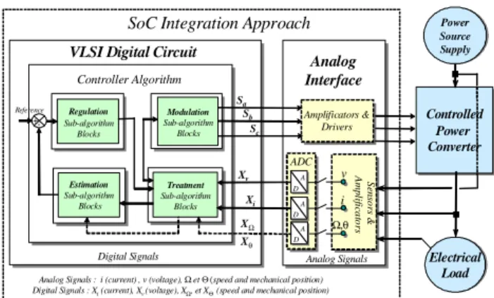
Figure 1 presents the structure of electrical systems. In the figure, the power environment and analogue interface are given as power source supply, controlled power converter, electrical load, sensors, amplifications, drivers and analogue to digital converters. The control algorithm is decomposed on four main functional blocks. Each block is done according its function and the hierarchy in the control algorithm [5]. The blocks are composed of independent and specific sub-algorithms which can be described by:
• treatment block: including sub-algorithms of
treatment and transformation models (as direct or reverse Concordia transformation, direct or reverse Park transformation, ...).
• estimation block : including sub-algorithms
of system estimation models (as flux and torque estimations, …).
• regulation block: including sub-algorithms of
regulation and control models (as hysteresis controller, PI controller, ...).
• modulation block: including sub-algorithms of
power modulation models (as three-phase sine function, space vector PWM, ...).
Xv Xi
A D
A D
A D
A D
A D
Ω,θ
v i
S
en
so
rs
&
A
m
p
li
fic
a
to
rs
ADC Amplificators &
Drivers
XΩ
Xθ
Digital Signals
Analog Signals : i (current) , v (voltage), Ωet Θ (speed and mechanical position) Digital Signals : Xi(current), Xv(voltage), XΩ, et XΘ (speed and mechanical position)
Controller Algorithm
Controlled Power Converter
Controlled Power Converter
Electrical Load
Electrical Load Sc
Sb Sa
Analog Signals VLSI Digital Circuit
Analog Interface SoC Integration Approach
Regulation
Sub-algorithm Blocks
Modulation
Sub-algorithm Blocks
Treatment
Sub-algorithm Blocks
Estimation
Sub-algorithm Blocks Reference
+-Power Source Supply
Power Source Supply
Figure 1.General structure of electrical system
3. MODULAR METHODOLOGY
3.1 Architectural Approach
IC architectureproposal is one of the most important hardware design steps. There are two main architecture approaches: the automatic and the dedicated approach.
Nowadays, designers generally use methods
based on behavioral synthesis principles to automatically extract a controller and an operative part by allocating operators and by arranging operations according to architecture constraints
[6].Behavioral synthesis is particularly adapted to
improve designer productivity and design quality, but is not considered universal for all applications and algorithms. Indeed, we can only generate optimized hardware amount and processing time
for homogeneous algorithm structures.
Consequently, the automatic approach is not a suitable solution for an IC-based electrical controller. Indeed, control algorithms used in most electrical drive applications are heterogeneous structures. All these technical restrictions can be resolved with a dedicated approach. However, it requires a longer development time and real designer know-how.
Finally, in order to generate an optimal architecture for an electrical controller and from electrical drives structure, we combined both approaches by applying modular principles generally used in IC conception.
3.2 Modular Principles
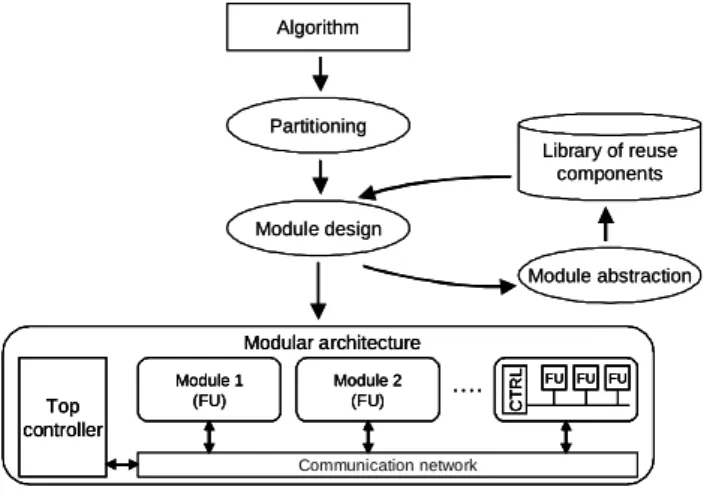
For verycomplex designs, modular conception is generally used to reduce design cycle. This methodology is based on hierarchy and regularity concepts. Hierarchy is used to divide a large or complex design into sub-parts that are more manageable. Regularity is aimed to maximize the reuse of already designed components and subsystems [7]. The modular partitioning is generally guided by precise rules that are resumed in three main steps in design-flow [6]:
• Partitioning: The partitioning can be applied in order to split the system into simpler modules. This step allows producing a hierarchical modular decomposition of the initial system.
• Module design: Each module generated can be
designed independently using a specific library of components. It may include either existing functional units or specific modules that have been designed during previous steps for example, arithmetic operators as multiplier, divider … etc.
• Module abstraction: The abstraction of the module has to be done in order to enable its reuse as a complex library element.
The result of such a design flow is a modular architecture made up of control unit (called the top
controller) managing a set of modules (functional units FU) and linked by a communication network as illustrated in Figure 2. This architecture may be hierarchical and the composition of each functional unit may consist of another control unit and another set of functional units, and so on. The hierarchy ends with functional unit without local control, such as a basic arithmetic operator.
Module abstraction Module design
Partitioning Algorithm
Library of reuse components
Top controller
C
T
RL FU FU FU
Module 1 (FU)
Module 2 (FU)
Communication network
….
Modular architecture
Module abstraction Module design
Partitioning Algorithm
Library of reuse components
Top controller
C
T
RL FU FU FU
Module 1 (FU)
Module 2 (FU)
Communication network
….
Modular architecture
Top controller
C
T
RL FU FU FU
C
T
RL FU FU FU
Module 1 (FU)
Module 2 (FU)
Communication network
….
Modular architecture
Figure 2.Modular design flow
4. MODULAR DESIGN FOR ELECTRICAL CONTROLLER
Like presented earlier, the idea of the modular methodology is to decompose the algorithm into modules that are separately designed, tested and included in the architecture. It means to reduce the development cost of complex algorithms as electrical controller. However, it is necessary to adapt the methodology to particular constraints of this application. To show the specificity of electrical controller, we will introduce an algorithmic partitioning how to structure the algorithm of electrical drives and after we will apply the modular principles to define a suitable architecture.
4.2 Modular Principles for Electrical
Controller
4.2.1 Partitioning
For the electrical controller, the partitioning step is split into two stages called algorithmic and architectural partitioning.
4.2.1.1 Algorithmic partitioning
The most current approach, used by VLSI IC designers to describe an algorithm before to propose the suitable architecture, is to apply Data Flow Graph DFG principles [8]. We briefly present the DFG representation mode, then
provide specific rules used for describe general electrical controller algorithms. Finally, a DFG-based algorithm example will be studied.
Data Flow Graph approach
In the basic version of a DFG, each node represents an operation which consumes data before its execution and produces data after its execution. This approach introduces an order between the reading of data’s on all inputs and the writing of resulting data’s on all output. An algorithm description of an electrical controller depends obviously on a very large variety of DFG. Indeed, the choice of the granularity is not without consequence on the controller performances. The thicker granularity (thick granularity) enjoys the facilities for an algorithm implementation and the design should be improved in terms of time to market. However, this approach not only increases the execution time but also the hardware amount. On the other hand, a thin granularity offers a good implementation potential in terms of low cost and control performances, but naturally complicates
strongly the design
.
DFG description rules
From previous considerations, and to help the designer to describe the suitable DFG of his algorithm, we elaborated five DFG description rules, as given by:
• Rule 1: First, give a DFG description of each
sub-algorithm block as referenced in the general structure of electrical controller, according to the following rules 2, 3 and 4.
• Rule 2: The nodes of the final DFG will
exclusively correspond to:
- basic arithmetic operators (thin granularity), - complex operators (thick granularity), existing in library,
- complex operators not in library, if those represent a homogeneous iterative algorithm
(for example, an integration by
accumulation...) and can be easily evolved.
• Rule 3: Between an existing thick grain and its
representation in thin granularity, the existing one should always be considered first. Moreover, when the constraints on execution time (delay) or integration density (hardware amount) are strong, the development in thin granularity is used. Thus, not only the hardware amount is reduced by sharing
execution time by increasing parallelisms of the algorithm.
• Rule 4: Analyze the parallelism of the
algorithm from its DFG representation. It
often generates periodic repetitions of
identical motifs operating on different data. These motifs give the possibility of a hardware optimization by sharing the data-path, i.e. Functional Units (FU).
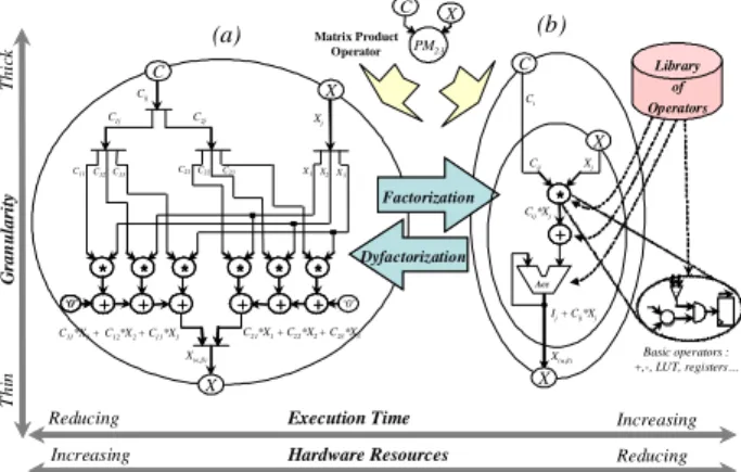
Case of the three-phases to two-phases
transformation algorithm
To illustrate these description rules
previously defined, we propose to compose from an algorithm commonly applied in electrical systems to transform a model expressed in
three-phases (X1, X2, X3) to two-phases (
Xα, Xβ
), asgiven by the relation (1):
= 3 2 1 23 22 21 13 12 11 X X X C C C C C C X X * β α(1)
This algorithm can be described at different levels of granularity according to the existing modules and to the conception constraints. So as seen in Figure 3, using the proceeding rules 2 & 3, the relationship (1) can be represented by a unique top. This top is the biggest existing operator in our
library, i.e. the matrix product PMij (i: row, j:
column) with i=2 and j=3, as given by the relation (2):
= 23 22 21 13 12 11 23 C C C C C CPM
(2)
However, to respect the delay and resource constraints, it could be necessary to decompose the operator in thinner granularity as multipliers and adders. At this new granularity level, respecting rules 2 and 4, we first try to parallelize the algorithm as much as possible. We can see such in the graph (a) of the Figure 3, which uses 6 parallel branches of multipliers and adders. Afterwards, by factorizing this repetitive pattern we obtain the graph (b) of the Figure 3, which reduces the hardware amount but in other hand increase the execution time. We can note that it is naturally possible to go down to lower level (i.e. logic gates). The final graph is thus a compromise between calculation time and resource amount, between factorization and dyfactorization (without factorization).
Ij+ Cij*Xj
C11C12C13
Xj
X1X2X3
X(α,β)
C21*X1+C22*X2 +C23*X3
C1j C2j
‘0’ C11*X1+C12*X2 +C13*X3
PM23
Basic operators : +,-, LUT, registers…
Reducing Execution Time Increasing
Increasing Hardware Resources Reducing
** ** ** ** ** ** + + ++ ++ ++ ++ ++ Matrix Product Operator T h ick T h in X C X Gr a n u la ri ty = Cij ‘0’ ‘0’ Dyfactorization Dyfactorization Factorization Factorization
C21C22 C23
X(α,β)
Xj
Cij*Xj ** + + X C Cij Acc Library of Operators Ci X (b) C X (a)
Figure 3.DFG representation of the relation(1)
4.2.1.2Architectural partitioning
At the architectural partitioning stage the hardware amount of modules is allowed. Thus, independent
modules, which compose final modular
architecture, are extracted by regrouping the different sub-algorithms previously identified in algorithmic partitioning. Five rules are proposed to define architectural partitioning. These rules take into account the main constraints of the final
IC: processing time, chip size, control
performance, design flexibility, integration
perspective and reusability. Finally, the five rules are:
• regrouping in the same module sub-algorithms
obtained from the similar functional block. The module thus developed can be proposed as a reused component of a design library.
• regrouping in the same module, sub-algorithms
using the most constrained hardware amount or processing time.
• regrouping in the same module, sub-algorithms
involve in analogue to digital and digital to analogue signal treatments, in a perspective of mixed analogue/digital integrated circuit.
• regrouping in the same module, sub-algorithms
which can be applied to improve control performance.
• regrouping in the same module, sub-algorithms
with homogeneous DFG. The aim is to use behavior synthesis to generate the architecture of this module.
Generally, these rules can not be used in same time because they are contradictory. In fact, the designer chooses the right one according to design constraints.
4.2.2 Module design
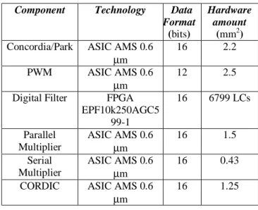
Partitioning and module design are closely inter-related. The hierarchical decomposition may be influenced by the set of already existing modules in the library of reuse components (regularity concept). On the other side, the selection of the modules is influenced by the hierarchical decomposition of the design. The power and flexibility of such scheme depend on the range of components that may be used in the library. For the electrical designer, the problem is summed up to initialize the design flow by defining an appropriate library of reuse components.From the sub-algorithms order defined at algorithmic partitioning, we have built a library of reuse components with two main categories as shown in Figure 4.
High level of granularity
Low level of granularity Concordia/Park
PWM
Digital Filter
Parallel
Multiplier Serial
Multiplieur
CORDIC
Figure 4.Library of reuse components
The first category is dedicated to complexes electrical controller sub-algorithms (thick grain) [9]. In our case, we have defined three components for standard electrical sub-algorithms of each algorithmic block, defined in electrical drives structure, as:
• Concordia/Park component corresponding to
treatment block.
• Digital filter component corresponding to
estimation and regulation blocks.
• PWM (Pulse Width Modulation) component
corresponding to modulation block.
The second category is dedicated to arithmetic operators (thin grain) [10] as:
• Parallel multiplier based on Booth2 algorithm.
This algorithm allows reducing multiplier execution time but increase hardware amount.
• Serial multiplier based on Baught-Wooley
algorithm. The serial multiplier has an optimized area rather than execution time.
• CORDIC (COordinate Rotational Integrated
Circuit) operator which execute rotational operation, dividing operation, logarithmic operation, ...
In order to validate each component of the library, an ASIC or FPGA integration of a prototype was made and results were resumed in Table 1 here after.
TABLE 1. The hardware integration results of reuse components
Component Technology Data Format
(bits)
Hardware amount
(mm2)
Concordia/Park ASIC AMS 0.6
µm
16 2.2
PWM ASIC AMS 0.6
µm
12 2.5
Digital Filter FPGA
EPF10k250AGC5 99-1
16 6799 LCs
Parallel Multiplier
ASIC AMS 0.6 µm
16 1.5
Serial Multiplier
ASIC AMS 0.6 µm
16 0.43
CORDIC ASIC AMS 0.6
µm
16 1.25
LC : Logic Cell
To reduce development cost, the library also includes a set of basic reused components as: storage units (memories, registers …) and communication units (multiplexers, switches …). All of the reuse components are described in VHDL language at register transfer level.
4.2.3 Module abstraction
The design reuseconsists to reuse components of any degree of complexity. In our case, these components are developed in VHDL at register transfer level. Thus; they can be reused as black boxes or macro-blocks such a design situation is illustrated in Figure 5.
Starting from a main algorithm and
partitioning steps, the designer use a set of components instances to build the modular architecture. From this design scheme, reused components with thick granularity are used as coprocessors in order to execute operations of main algorithm. In fact for the modular architecture, the synchronization is much less rigid than in the flat architecture as each module may run independently and in parallel with any other
module of the architecture. Communication between modules and the top controller allows
exchanging data according to predefined
protocols. We assume that all modules share a common clock. However, each module may have other local clocks. For a reused components with thin granularity (arithmetic operators), these components are used as a macro-blocks because they are defined as a functional unit without controller.
From this design flow, the main pieces of information necessary for the abstraction of a module for its reuse are:
- the operations it can execute,
- the communication protocol: control
signals, clock, …
- the timing scheme,
- the synthesis constraints.
Module abstraction Module design Main Algorithm Top controller C T
RLcpntFU FU
Module 1
(FU) Reused Compnt
Communication network …. Modular architecture cpnt cpnt cpnt Compnt Compnt Partitioning Algorithmic Architectural Thick granularity Thin granularity Algorithmic & architectural
partitioning rules
Library of reuse components Module abstraction Module design Main Algorithm Top controller C T
RLcpntFU FU
Module 1
(FU) Reused Compnt
Communication network …. Modular architecture Top controller C T
RLcpntFU FU
Module 1
(FU) Reused Compnt
Communication network …. Modular architecture cpnt cpnt cpnt Compnt Compnt cpnt cpnt cpnt Compnt Compnt Partitioning Algorithmic Architectural Partitioning Algorithmic Architectural Thick granularity Thin granularity Algorithmic & architectural
partitioning rules
Library of reuse components
Figure 5.Modular design flow for electrical
controller
5. MODULAR DESIGN VALIDATION
5.1 DTC Modular Decomposition
Tovalidate modular design flow for electrical controllers, we developed a modular architecture for an ASIC-based DTC (Direct Torque Control) algorithm of an asynchronous motor. Since, DTC structure is simple; it can be used to several AC motor types (asynchronous, synchronous ...). This control method insures excellent speed or torque control without any mechanical information. Moreover, sensitivity to machine parameters is lower for the DTC in comparison with classic vector control structures [11].
To make the validation, we consider a set of integration constraints such as:
- Integrate DTC controller into ASIC target
in a perspective of mixed analogue/digital integrated circuit.
- Increase the DTC control performances
using the specificity of hardware
integration.
- Improve development time
From the DTC algorithm and DFG description rules previously presented (paragraph 3.2.1.1), we define at algorithmic partitioning step 4 sub-algorithm blocks as illustrated in data flow graph of Figure 6.
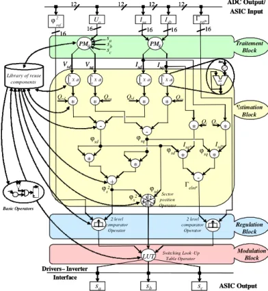
sb sa
Uo
sc
Drivers – Inverter Interface 12 sa sb sc 16 16 16 16 ϕ2 ref 2 level comparator Operator
Switching Look -Up Table Operator
ADC Output/ ASIC Input
PMij PMij
Isa Isb Γref*
LUT
16
2 level comparator
Operator
12 12 12
-Isd Isq
Vsq
-Vsd
ϕsd ϕsq
*
* +
* Qi
ϕs2
*
-Isq*
ϕsd ϕsq
1 3 2 5 6
* * * *
Qvd Qvq Qid Qiq
Γelm*
∫t 0Xdt ∫
t
0Xdt ∫
t 0Xdt ∫
t 0Xdt
Sector position Operator ϕsd ϕs2
acc + z-1 X(t) acc + z-1 X(t) 4 * * Isd* Qi ASIC Output Estimation Block Traitement Block Regulation Block Modulation Block Basic Operators
Library of reuse components
Figure 6.Data flow graph of DTC algorithm
The treatment block encloses two Concordia transformations which are represented with thick grain operators. These operators correspond to the matrix product of Concordia.
The estimation block includes
sub-algorithms which compute flux
(
ϕ
s,
ϕ
sd,q), torque
(
Γ
elm) and flux sector position (
δ
).
The DFG of this block is defined with thin grain arithmetic operators as: adder, multiplier…The regulation block contains two similar
sub-algorithms, torque and flux hysterisis
comparators, characterized with thick grain operators called 2 level comparator operator. The modulation block includes drivers switching table. It represented with thick grain operator named switching look-up table operator.
The DTC algorithm is implemented with 16 bits data format. We choose this format following previous study presented in [12, 13].
Now, the design constrains and DFG of DTC algorithm are fixed, we regroup, at architectural partitioning step, the four sub-algorithm blocks in three modules according to the rules presented in paragraph 3.2.1.2.
• Interface module: the direct Concordia
transformation sub-algorithm is proposed to build a unique module called the interface
module. Indeed, this sub-algorithms is
involved, via the sensors/amplifiers and the ADC of the control system, in an analogue to digital signal treatment. Thus, the module can be considered in a viewpoint of mixed analogue/digital integrated circuit. Moreover, in reuse perspective, the sub-algorithm can be included in a generic module regrouping other transformation algorithms used in electrical
control algorithms as Clarke or Park
transformations. The architecture of the module contains a functional unit and a local control unit. The functional unit is composed by a look-up table (LUT) and a set of reuse thin grain components as: adder/substractor, shift register …. Thus, the hardware amount of the architecture is optimized. In fact, the LUT and shift register avoid using the multiplier operator to compute the matrix product. The local control unit is employed to manage the ADC and the data in the FU.
• Computation module: motor model
sub-algorithms require the most important
hardware operator resource in opposite to the others controller sub-systems. Therefore, we choose to regroup all these sub-systems in one module, called computation module, in order to optimize the hardware amount of the final chip. To design this module, only one functional unit describes the architecture of the computation module which is composed by: an Arithmetic
Logic Unit ALU (32-bit/32-bit
Adder/Susbtractor, a 32*16-bit Multiplier based on reuse parallel multiplier and a transmission operator to transfer data’s between registers), a specific register-file (8 registers of 16-bit and 4 registers of 32-bit), and finally a ROM of constants.
• Control module: output data’s of the switching
logic table sub-algorithm are involved, via the amplifiers and inverter drivers, in a digital to analogue signal treatment. Furthermore, the two simple hysteresis controllers are similar
sub-algorithms. They can be regrouped with the flux zone position and the switching logic table sub-systems in a same module in order to
improve control performances of DTC
algorithm such as presented here. The architecture is built with a functional unit without control and composed of 3 operators: a position estimator, a hysteresis controller and a LUT.
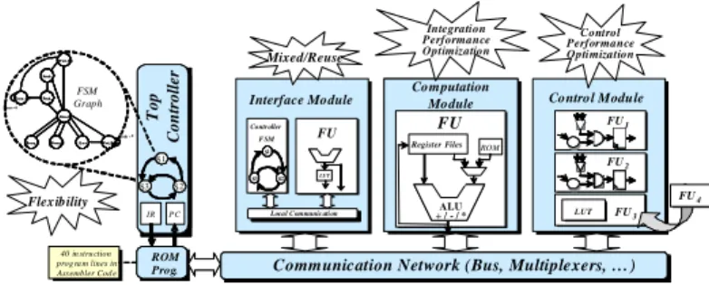
The top controller of the modular architecture is applied to control the FU of computation module. It also used to manage data transmission with the two other modules (Interface and Control). In order to optimize the top controller architecture and circuit debugging, a programming approach by microcode is proposed [14]. Also in order to compare the performances of the architecture, two kinds of controller were developed: controller with finite state machine (FSM) and controller with pipeline. The pipeline controller works at 25 MHz (1 instruction/40ns clock cycle). The figure 7 shows the modular architecture of DTC algorithm.
Communication Network (Bus, Multiplexers, …)
S1 S3 S2 S1 S3 S2 T op C o n tr o ll er PC IR ROM Prog. FU ROM Register Files ALU + / - / *ALU + / - / * Computation
Module W ai t_ Ini t
Fet ch _ 0
Fet ch _ 1 E rror_ Ovf
Déco d e
E xe c Wa it_ Re a dy B rea q_ N B rea q _Z
Re a dy = 0 Re se t = 0
W ai t_ Ini t
Fet ch _ 0
Fet ch _ 1 E rror_ Ovf
Déco d e
E xe c Wa it_ Re a dy B rea q_ N B rea q _Z
Re a dy = 0 Re se t = 0
40 in stru ction prog ra m lines in Assembler Cod e
S1 S3 S2 S1 S3 S2 Controller FSM Interface Module FU LUT Local Communic ation
Control Module FU2 FU1 FU3 LUT FU4 FSM Graph Flexibility Mixed/Reuse Integration Performance Optimization Control Performance Optimization
Figure 7.DTC modular architecture
5.2 DTC Validation
To validate the DTCmodular architecture, we have developed a mixed analogue/digital simulation based on HDL languages for the DTC controller and its electrical environment [15]. In fact, the power environment and analogue interface (sensors, analogue to digital converter, load…) are described in
SpectreHDL and DTC architecture in VHDL.
5.2.1 Improving Torque Control by DTC
architecture modification
Identification of DTC control defaults
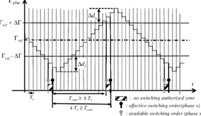
In order to respect technical constraints of power inverter, the sample period of the controller should never exceed the switching limit given by the manufacturer. However, it is well-known that in
those sampling conditions, precision of control and stability are not satisfactory. It is particular true in the case of the DTC which used hysteresis controllers to correct torque regulation. Thus, ripples can be observed on the controlled torque which can be reflected on the driving shaft and caused damage on the structure [16]. Many researches in literature propose several control strategies or new structures to limit those effects [17- 19]. However, the proposed solutions always increase the controller algorithm complexity which is restricting for ASIC integration in terms of hardware amount and execution time.
New DTC strategy based on hardware solution
To improve DTC regulation and decrease torque ripples, we propose to reduce the sampling period of the controller, as much as possible. Thus, torque derivation could change faster than previously, avoiding consequently important torque overtaking. In the other hand, latency of electrical systems, using power inverter, is not low enough to justify high sampling frequency. However, by including an authorization mode in the original DTC strategy, only suitable and required signals will be propose to control switches of the inverter associated to the induction
motor. Thus, a minimal sampling period (Tcom)
should be fixed and never be shorter than a
sampling period multiple (k Te). In the opposite
case, the control signal transmission would not be authorized, as shown in the Figure 8.
: no switching authorized zone : effective switching order(phase x)
Γref Γref-∆Γ
Γelm
k Te≥Tcom
Γref+ ∆Γ
Te
t
∆du
∆dl
Tcom≥k Te
: available switching order (phase x)
Figure 8.Torque response based on new DTC
strategy
New control module architecture
Control Module architecture must be composed in part with elements of the previous DTC architecture, as torque and flux hysteresis comparators, position flux estimator and switching control Look-Up Table (LUT). And in another
part with elements of the new architecture which can be carried out from rudimentary components, as shown in the Figure 9.
Sa
Sc(k)
δ
1 0
π
1 0
1 6 5 4
321
6 5 4
32
Switching Look-up
Table π
τ Γelm
ϕs
ϕsd,q
ϕs
Γref
ϕref
τ
Mux DQ Mux DQ Rudimentary components
Rudimentary components
Mux DQ Mux DQ
Sb
Sc Sb(k)
Sa(k)
Tc om Tc om
Tco m Tco m
Tc om Tc om
≠≠ ≠≠ ≠≠
Sc(k-1)
Sb(k-1) Sa(k-1)
A
u
thorization Block
Comparison Block
Decision Block
Figure 9.Control Module architecture
Three new elements will be added to the previous Control Module architecture, so called
decision block, authorization blocks, and
difference bocks. The decision block receives information from authorization blocks and difference bocks. Thus, difference blocks allow to detect difference between switching control
signals Sa,b,c at sampling periods (k-1) and (k). In
case of difference, the decision bock will applied the new control signal, on condition that authorization blocks authorize signal generation. In the opposite, the control decision will be reported at the next sampling period (k+1). Once switching control signal sent, authorization bocks is fixed to prevent any new sending during a
minimal switching period (Tcom) which is given in
specification of the control system.
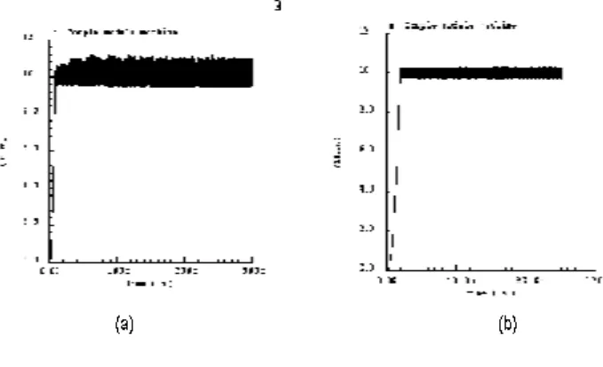
Validation results
Figures 10(a) and 10(b) show torque regulation performances with previous and new DTC strategy. The torque is controlled around its reference 10 N.m with a simple hysteresis correction: +/- 0.25 N.m for a flux reference: 0.8 Wb. In case of new control method, sampling and minimal switching periods are respectively given
by Te= 2µs and Tcom= 30µs.
To validate contribution of new DTC strategy in torque control performances, a torque resultant value was estimated. Thus, a significant reduction of torque overtaking can be observed since it reaches only 0.25 % instead of 6.75 % with classic DTC method.
Finally, the modular structure allows improving performances of the whole modular architecture by a simple local modification. In a perspective, many applications can be considered with the modular approach as predict control.
Figure 10. Instantaneous torque response obtained
from HDL models
(a) classic DTC method ; (b) DTC with new control strategy
Experimental validation
The architecture was validated by using the test-bench engine of the Figure 11-a. This test-bench is mainly constituted by an asynchronous engine (Figure 11-c) and an in-house card based on ATERA Flex 10K100A RC240-1 FPGA (Figure 11-b).
a)
b) c)
a)
b) c)
Figure 11. Experimental test-bench
(a)test-bench ; (b) in-house FPGA electronic card ; (c) engine
The Figure 12 presents experimental results. Figures 12-a and 12-b show the starting up until the established phase, the evolution of torque and
rotor flux constituents φq and φd, respectively. The
Figure 12-c presents φq = fct (φd)
a) b) c)
a) b) c)
Figure 12. Experimental results
(a) torque ; (b) rotor flux φq and φd ; (c) φq = fct (φd)
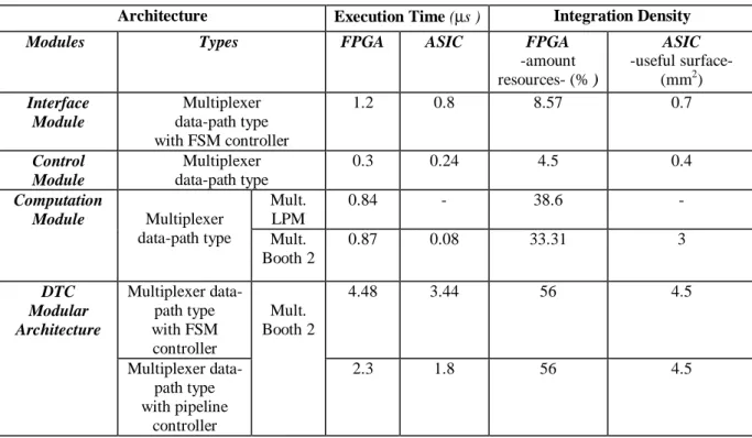
5.2.2 Hardware Implementation Results
The Table 2 compares FPGA and ASIC hardware
solutions by implementing modular DTC
architecture on an Altera Flex 10K100 FPGA (3V,
25 MHz) and on a AMS 0.6 µm ASIC (3.3V, 25
MHz). In the case of FPGA target, we also
compare, for computation module, the
performances obtained with LPM multiplier from Altera’s library of parameterized modules and our reuse multiplier based on Booth2 algorithm.
The FPGA hardware resources rate is nearly 56% with approximately 2496 logic cells used for 4992 available. The execution time of the circuit can reach 2.3µs (pipeline controller) for at least 4,48µs (FSM controller). As expected, ASIC implementation results are much better in term of speed processing with 1.8 µs (pipeline controller) for at least 3.44µs (FSM controller). In term of integration density, a useful integrated surface
reaches 4.5 mm2.
As planned, size of the computation module of the DTC architecture is much bigger than Interface Module and Control Module. In detail, adder/subtraction and multiplier operators used in the Computation module are respectively based on Carry Look-Ahead and Booth2 algorithms which constitute respectively 10% and 75% of the size chip. Moreover, the execution time of the computation module given in Table 2 represents the time for a multiplication operation with the result stored in the register file.
TABLE 2. FPGA and ASIC Integration results for DTC implementation
Architecture Execution Time (µs ) Integration Density
Modules Types FPGA ASIC FPGA
-amount resources- (% )
ASIC
-useful surface- (mm2)
Interface Module
Multiplexer data-path type with FSM controller
1.2 0.8 8.57 0.7
Control Module
Multiplexer data-path type
0.3 0.24 4.5 0.4
Computation
Module Multiplexer data-path type
Mult. LPM
0.84 - 38.6 -
Mult. Booth 2
0.87 0.08 33.31 3
DTC Modular Architecture
Multiplexer data-path type with FSM controller
Mult. Booth 2
4.48 3.44 56 4.5
Multiplexer data-path type with pipeline
controller
2.3 1.8 56 4.5
The different hardware results show that the
developed architecture is in excellent
appropriateness with the modular partitioning applied to DTC algorithm. The Figure 11 shows the final DTC ASIC layout with the new control strategy for AMS 0,6µm technology. Benefit of the modular approach is shown.
C om putation M odule
C on trol M o du le Inte rfa ce
M o d ule
T o p C o ntroller
C om putation M odule
C on trol M o du le Inte rfa ce
M o d ule
T o p C o ntroller
5.2.3 Reuse results
In order to prove the interest of the modular methode to reduce conception time, we have developed a DTC architecture based on reuse Concordia/Park component (thick grain in the library of reuse components). Thus, the interface module was replaced with Concordia/Park component without modification of the other modules. In order to measure the profit in conception time, we use the simple relation (3) given by:(
Number of modules * 100)
Profit=
Number of reused modules
(3)
In the case of DTC controller, the profit reaches 33%.
Table 3 compares the ASIC results for both DTC architectures.
Figure 11.Final ASIC Layout of DTC modular
TABLE 3. ASIC integration results for DTC architecture based on with/without reuse Concordia/Park component.
DTC Technology Data
(bits) Clk (ns) Execution Time (µs)
Hardware Amount (mm2) Without thick
grain
AMS 0.6 µm 16 20 1.8 8.7
With thick grain
AMS 0.6 µm 16 20 1.8 11
The results are in accordance with the granularity effect developed in 3.2.1.1. In fact, the thicker Concordia/Park component allows reducing design time but increasing the hardware amount of the final architecture.
6. CONCLUSION
In this paper, the authors develop a new architecture approach for electrical controllers. They propose to apply modular design principles quite well-known nowadays in microelectronic industry. Specific modular partitioning principles were defined, and then these modules are regrouped into a modular architecture. The methodology developed is principally based on a library of reuse components. In fact, we have developed library of reuse components in two categories: high and low level of granularity. This approach was then used to design an ASIC integrated solution for a vector control structure called DTC. Three modules are identified and the architecture of each of them described. In order to reduce debugging time and improve design flexibility, a specific programmable architecture based on a microcode is proposed. Finally, the modular architecture optimized both hardware amount and processing time, making easier design reuse of circuit was presented. This example of modular development is shown to prove the contribution of the proposed approach
in improving hardware results, controller
performances and conception time that reach 33% compared with classic design.
7.
REFERENCES
1.Cecati, C., “Microprocessors for Power Electronics and Electrical Drives Applications”, Newsletter, IES Industrial Electronics, Vol. 46, No. 3, (1999).
2. Le-Huy, H., “Microprocessors and Digital IC’s for Motion Control”, proceedings of the IEEE, Vol. 82, (1994), 1140-1163.
3. Tzou, Y.Y. and Jyang, J.Y., “A programmable current vector control IC for AC motor drives”, The International Conference on Industrial Electronics, Control and Instrumentation (IEEE IECON’99), San Jose, USA, (1999), 216-221.
4. Riesgo, T., Torroja, Y. and Dela Torre, E., “Design Methodologies Based on Hardware Description Languages”, IEEE Transactions on Industrial Electronics, Vol. 46, (1999), 3-12.
5.De Doncher, R. and Novotny, D.W., “The universal field oriented controller”, The Industry Applications Society conference (IEEE IAS’88), (1988), 450-456.
6.Jerraya, A.A., Ding, H., Kission, P. and Rahmouni, M., “Behavioral synthesis and component reuse with VHDL” ,Kluwer Academic Publishers, (1997).
7.Trimberger, T., Rowson, J.A., Lang, C.R. and Gray, J.p., “A structured design methodology and associated software tools”, The IECS conference (IECS’1981),
Vol. 28, No. 7, (1981).
8. Lavarenne C., et Sorel Y., Modèle Unifié pour la Conception Conjointe Logiciel-Matériel », Revue Traitement du Signal, Vol. 14, No. 6, (1997), 569-578. 9. Kebbati, Y., “Développement d’une méthodologie de
conception matériel à base de modules génériques VHDL-VHDL-AMS en vue d’une intégration de systèmes de commande électriques”, Phd Thesis, Strasbourg, France, (2002).
10. Souffi, H., “Conception d’opérateurs numériques réutilisables: application à une méthodologie d’implantation rapide et optimale d’algorithmes de commandes”. Phd Thesis, Strasbourg, France, (2002). 11. Takahashi, I. and Noguchi, T., “A new quick response
and high efficiency control strategy of an induction motor” The Industry Applications Society conference (IEEE IAS'1985), (1985), 495-502.
12. Chapuis, Y.A., Girerd, C., Aubepart, F., Blonde, J.P., et Braun F., “Quantization Problem Analyze on ASIC-Based Direct Torque Control of an Induction Machine”,
Actes de IEEE Industrial Electronics, Control and Instrumentation (IECON), Aachen, Germany, (1998), 1527-1532.
13. Kebbati, Y., Girerd, C., Chapuis, Y.A., et Braun F., “Advances in FPGA/ASIC Digital Integration Solutions for Vectors Control of Motor Drive”, Actes de IEE International Power Electronics and Converter Conference (IPEC), (2000), 1177-1182.
14.Kebbati, Y., Girerd, C., Chapuis, Y.A., et Braun F., “Advances in FPGA/ASIC digital integration solutions for vector control of motor drive” The International Power Electronics and Converter conference (IEEE IPEC'2000), Tokyo, Japan, (2000), 1177-1182. 15. Girerd C., Aubépart F., Poure P., Blondé J.P., Chapuis
Y.A., et Braun F., « Modélisation VHDL/Spectre HDL et Simulation Mixte sous Cadence : Conception d’un ASIC de Commande de Moteur Asynchrone », Actes des Journées Thématiques sur l’Adéquation Algorithme Architecture du GDR ISIS, (1999). 16. Casadei D., Grandi G., Serra G., et Tani A., « Effects
of Flux and Torque of Induction Machines Based on Stator Flux Vector Control », Actes de IEEE Industrial Electronics, Control and Instrumentation (IECON), Bologna, Italia, (1994), 299-304.
17.Kang, J.K. and Sul, S.K., “New Direct Torque Control of Induction Motor for Minimum Torque Ripple and Constant Switching Frequency”, IEEE Transactions on Industrial Applications, Vol. 35, (1999), 1076-1082.
18. Martin, C.A., Roboam, X., Meynard, T.A. and Carvalho, A.S., “Multi-level Direct Torque Control with imposed switching frequency and reduced ripples”, IEEE Power Electronics Specialists Confrence (IEEE PESC’2000), Galway, Ireland, (2000).
19. Vaez-Zadeh, S. and Mazarei, G.H. “On Line Determination of Optimal Hysteresis Band Amplitudes in Direct Torque Control of Induction Motor Drives”
International Journal of Engineering, Transactions A: Basics, Vol. 15, No. 4, (2002), 329-338.