Technology (IJRASET)
Design of Single Master Inter-Integrated
Circuit Bus Controller
Anagha. A1, M. Mathurakani 2
1
M.TECH Student, 2 Professors, Dept. of Electronics & Communication Engineering
Toc H Institute of Science and Technology, CUSAT, Kerala
Abstract— Inter-Integrated Circuit Bus commonly known as IIC or I2C Bus was developed by Philips semiconductors. I2C is a multi-master, multi-slave, single-ended, serial computer bus and is typically used for attaching lower-speed peripheral ICs to processors and microcontrollers. The I2C bus physically consists of 2 active wires called SDA and SCL which are bi-directional. SDA is the Serial Data Line and SCL is the Serial Clock Line. Each slave connected to the I2C bus has its own unique address. In this paper, a single master – single slave Inter-Integrated Circuit bus has been developed. An EEPROM has been used as the slave device.The design was based on Finite State Machine using VHDL and was simulated using ModelSim.
Keywords— Integrated Circuits, FSM, Master, Slave, EEPROM, SCL, SDA.
I. INTRODUCTION
The I2C bus was invented during early 1980's by Philips Semiconductors to provide an easy way to connect a CPU to peripheral chips in a TV-set.Thus I2C bus reduced the complexity of the system , just by using 2 wires SCL and SDA.Other protocols like RS-232, SPI, RS-422,that require more pin connection in the IC(Integrated Circuit) for serial data communication to take place, as the physical size of IC have decreased over the years, we require less amount of pin connection for serial data transfer I2C protocol can overcome this problem which requires only two lines for communication with two or more chips and can control a network of device chips with just a two general purpose I/O pins whereas, other bus protocols require more pins and signals to connect devices. The I2C bus is a multi-master bus. This means that more than one IC capable of initiating a data transfer can be connected to it.
II. OVERVIEWOFI2CPROTOCOL
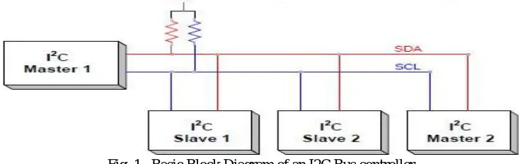
[image:2.612.122.493.478.594.2]The I2C is a two-wire serial bus as shown in figure 1, making it cheap and simple to implement in hardware.The two I2C signals are serial data (SDA) and serial clock (SCL). Together, these signals make it possible to support serial transmission of 8-bit of data-7-bit device addresses plus one control data-7-bit over the two-wire serial bus. The device that initiates a transaction on the I2C bus is termed as the master. The master normally controls the clock signal. A device being addressed by the master is called a slave.
Fig. 1 Basic Block Diagram of an I2C Bus controller
The I2C protocol supports multiple masters, but most system designs include only one. There may be one or more slaves on the bus. Both masters and slaves can receive and transmit data bytes. Each I2C-compatible hardware slave device comes with a predefined device address, the lower bits of which may be configurable at the board level. The master transmits the device address of the intended slave at the beginning of every transaction. Each slave is responsible for monitoring the bus and responding only to its own address. This addressing scheme limits the number of identical slave devices that can exist on an I2C bus without contention, with the limit set by the number of user-configurable address bits (typically two bits, allowing up to four identical devices).
transmission mode, after the initiation of the START sequence, the master sends out a slave address. The address byte contains the 7 bit slave address, which is followed by the direction bit (R/ w). After receiving and decoding the address byte the device outputs Acknowledge on the SDA line. After the slave device acknowledges the slave address + write bit, the master transmits a register address to the slave this will set the register pointer on the slave. The master will then begin transmitting each byte of data with the slave acknowledging each byte received. The master will generate a stop condition to terminate the data write.
[image:3.612.154.479.165.242.2]
Fig 2: Master Transmission mode
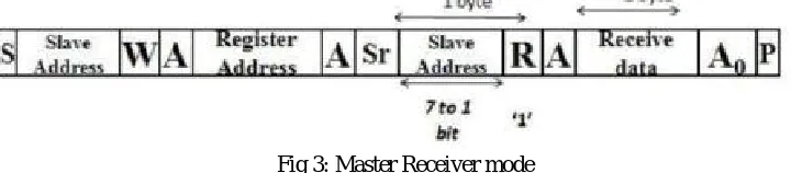
In master receiver mode, the first byte is received and handled as in the master transmission mode. However, in this mode, the direction bit will indicate that the transfer direction is reversed. Serial data is transmitted on SDA by the slave while the serial clock is input on SCL. START and STOP conditions are recognized as the beginning and end of a serial transfer (Figure 3). The address byte is the first byte received after the start condition is generated by the master. The address byte contains the 7-bit slave address, which is followed by the direction bit (R/ w). After receiving and decoding the address byte the device inputs acknowledge on the SDA line. The slave then begins to transmit data starting with the register address pointed to by the pointer. If the register pointer is not written before the initiation of a read mode, the first address that is read is the last one stored in the register pointer. The slave must receive a “not acknowledged” to end a read.
Fig 3: Master Receiver mode
IV.DESIGNIMPLEMENTATION
I2C master controller is designed using VHDL based on Finite State Machine (FSM). The algorithm of the FSM is explained below:-
A. Algorithm
State 1: Ready condition: I2C bus doesn‘t perform any operation.(SCL and SDA remains high) and enable is low. If Ena becomes HIGH it enters into next state.
State 2: Start condition: When ena is HIGH, Master initiates data transmission by entering into the next state adr.
State 3: Adr state: In this next adr state, master sends the slave address serially to the slave. Bit_cnt is used as counter to count the bits of address transferred and as it becomes 0,it enters into next state.
State 4: Ack state: If the slave address matches with the slave it sends an acknowledgement bit in response to the master. Now R/W bit is checked if it is LOW, it enters write state else read state.
State 5: Write state: The 8 bit data to be transmitted is sent to the slave by the master. After receiving the data, slave acknowledges the master.
State 6: Read state: The 8 bit data is read from the slave by the master. After reading the data, acknowledgement is sent. State 7: Stop condition: After the transmission of the data, STOP bit is sent.(SCL is high and SDA is from Low to high).
B. Finite State Machine (FSM)
[image:3.612.129.489.383.462.2]Technology (IJRASET)
Fig 4: FSM for single master I2C bus controller
V. SIMULATIONANDRESULTS
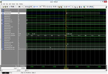
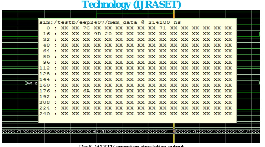
Here, EEPROM 24CXX Series is used as the slave. The simulation is done using ModelSim and verified the simulation results for READ and WRITE operations in the EEPROM. Figure 5 and Figure 6 shows the simulation outputs for READ and WRITE cycles respectively.
[image:4.612.91.525.402.700.2]Fig 5: WRITE operation simulation output
VI.CONCLUSION
The design for a single master I2C bus controller was developed successfully and the simulation of the design was done using ModelSim. The master performed READ and WRITE operations by making EEPROM 24CXX series as the slave device. This design successfully performed the READ and WRITE operations using I2C bus and the output waveforms were verified. This design can be expanded into multi-master design in future which will be more useful in connecting more peripheral devices.
AUTHORPROFILE
REFERENCES
[1] Philips Semiconductor, “ I2C Bus Specification”, April 1995.
[2] Frederic Leens, “An Introduction to I2C and SPI Protocols”, IEEE Instrumentation & Measurement Magazine, pp. 8-13, Feb 2009. [3] Peter Corcoran, “Two Wires and 30 Years”, IEEE Consumer Electronics Magazine, pp. 30- 36, July 2013.
[4] Kangshun Li, Yan Chen and Hezuan Liu, “A New Method of Evolving Hardware Design Based on IIC Bus and AT24C02”, IEEE, Proceedings of the 10th World Congress on Intelligent Control and Automation July 6-8, 2012, Beijing, China.
[5] Embedded System Design: A Unified Hardware/Software Introduction Frank Vahidand Tony Givargis ,John Wiley & Sons; ISBN: 0471386782.
ANAGHA A: She has received her B-Tech degree in Electronics and Communication Engineering from University of Kerala, Kerala, India in 2014. Currently she is pursuing her M-Tech Degree in Electronics and Communication Engineering with specialization in VLSI and Embedded System in Toc H Institute of Science and Technology, Cochin University of Science and Technology (CUSAT), Kerala, India. Her area of research interest includes Embedded System Design and Signal Processing.