DESIGN AND ANALYSIS OF LOW POWER
HYBRID ADDER
1M.JAYAPRAKASH, 2Dr.A.SHANMUGAM ,3 M.Peer Mohamed
1Asst.Prof., Department of ECE,SCAD Institute of Technology, Coimbatore
2Principal,Department of ECE, Bannari Amman Institute of Technology, Sathyamangalam.
3Asst.Prof., Department of ECE,SCAD Institute of Technology, Coimbatore
E-mail: [email protected]
ABSTRACT
For any digital system, digital signal processing or control system addition is a core operation. The performance of the resident adders greatly influences rapid and accurate operation of digital systems. Adders are one of the most prominent components in digital systems, as they are broadly used in other basic digital operations such as subtraction, multiplication and division. Improved the performance of the adder would therefore greatly advance the execution of operation greatly advance the execution of operations inside a circuit compromised of such blocks [1]. A comparative analysis on power consumption in three different adders, each offering different advantages and having tradeoffs has been performed based on circuit complexity and power consumption. The pioneer of CMOS traditional adder circuits, which consumes more power when compared to other two adders. The total number of transistors required for conventional CMOS adder is 28. Recently, it has been proved that the multiplexer-based multiplier outperforms the modified Booth multiplier both in speed and power dissipation by 13% to 26%, due to small internal capacitance [2]. The performance characteristics of conventional multiplier types which observed, it is found that the multiplexer-based and Transmission Gate based multiplication algorithm is more advantageous, especially when the size of the multiplied numbers is small. The number of transistors required for multiplexer based adders is 16. A heuristic approach, known as hybrid adder models is proposed to achieve optimal power savings at smaller geometry sizes. This hybrid adder model that consumes low power among three adders and the transistors required are 12. The design is simulated using MOSIS 90nm technology.
Keywords: Full Adder, Hybrid Adder, CMOS, Multiplexer, MOSIS
1. INTRODUCTION
The well-engineered deep submicron CMOS technologies are explored to address the challenging criteria of these emerging low-power and high-speed communication digital signal processing chips. The performance of many applications as digital signal processing depends upon the performance of the arithmetic circuits to execute complex algorithms such as convolution, correlation, and digital filtering [3]. In very-large-scale integration (VLSI) systems, there are most frequently and widely used circuits namely fast arithmetic computation cells including adders and multipliers. The most efficient implementation of simple gates (e.g. NAND/NOR) which have only a few transistors and nodes and a small delay due to single inversion level, are allowed by conventional CMOS. The large PMOS transistors have some disadvantages that result in high input capacitances and area requirements, and the weak output driving
capability caused by series transistors. The conventional CMOS adder is designed in tanner
s-edit and the circuit is simulated. When compared to
multiplexer based adder and hybrid adder, the power consumed by the conventional CMOS adder is high because the transistors count is high which may lead to large dynamic power dissipation, due to this the circuit will draw more power. Parallel combination of p-mos and n-mos are used in multiplexer based adder. For designing a 4:1 multiplexer full adder 16 transistors are required. Similar to conventional CMOS adder the multiplexer based adder is designed in tanner s-edit and the circuit is simulated. The power consumed
by multiplexer based adder is less than
2. ADDER TOPOLOGIES
Adder is the core element of complex arithmetic circuits like addition, multiplication, division, exponentiation, and so forth. There are standard implementations with various logic styles that have been used in the past to design full adder cells [1][4][5] and the same are used for comparison in this paper. Although they all have similar function, the way of producing the intermediate nodes and the transistor count is varied. Different logic styles tend to favor one performance aspect at the expense of the others. As addition forms the basis of many binary operations, adder circuits are of great interest in digital design. With the purpose to fulfill the various speeds, power and area requirements of implementations, a wide variety of adder circuits have been proposed in literature. As the most frequently used block in the overall design is full-adder, we turn our attention to design an efficient full-adder, which operates with the possible power consumption. Power is one of the essential resources, so the designers try to save it while designing a system. Power dissipation depends upon the switching activity, node capacitances, wire capacitances and control circuit size [2]. At the device level, reducing the supply voltage VDD and reducing the threshold voltage accordingly would reduce the power consumption. Scaling the supply voltage appears to be the well-known means to reduce power consumption. However, lower-supply voltage increases circuit delay and degrades the drivability of the cells designed with a certain logic style. One of the most significant obstacles in decreasing the supply voltage is the large transistor count and Vth loss problem. By selecting proper (W/L) ratio we can minimize the power dissipation without decreasing the supply voltage [6].
2.1 Conventional CMOS Adder
The 28 Transistor full adder is the pioneer CMOS traditional adder circuit. The schematic of this adder is shown in Figure 1.This adder cell is built using equal number of N-fet and P-fet transistors[11]. The logic for the Complimentary MOS logic was realized using the Equations.(1) and (2),
[image:2.612.318.522.101.288.2]Carry= AB+BC+AC (1) Sum = A B C (2)
Figure 1: Schematic Of Conventional Cmos 28-T One-Bit Full-Adder
The first 12 transistors of the circuit produce the Carry and the remaining transistors produce the Sum outputs. Therefore the delay for computing
Cout is added to the total propagation delay of the
Sum output. The structure of this adder circuit is huge and thereby consumes large on-chip area [7].
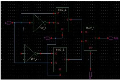
2.2 Multiplexer Based Adder
Figure 2: Multiplexer Based Adder
[image:2.612.310.521.413.553.2]design, creating a 2-to-1 MUX tree does not bring any drawback by means of speed or power dissipation [8]. The schematics of the cascaded block are given in Figure 2.
2.3 Hybrid Adder
The transistor connection for a complementary switch or transmission gate consists of an n-mos and p-mos transistor connected in parallel with separate gate connection. The control signal is applied to the gate of n-mos, and its complement is applied to the gate of the p-mos device[9]. The operation of transmission gate can be best explained by considering the characteristics of both the n-device and p-device as pass transistor individually. We will address this by treating the charging and discharging via transmission gate. n-mos pass transistor is good for transmission of ‘1’ and poor for transmission of ‘0’.p-mos pass transistor is good for transmission of ‘0’ and poor for transmission Of ‘1’. The circuit of the 12 pass transistor adder is shown in figure 3. If the signal degradation at the SUM and CARRY is significant for deep sub-micron circuits, drivers can be used to reduce the degradation. The driver will help in generating outputs with equal rise and fall times. This results in better performance regarding speed and low power consumption. The output voltage
swing will be equal to the VDD, if a driver is used at
the output.
Figure 3: Hybrid 12 Transistor Adder
3. COMPARISON
Here the performance measurement of conventional CMOS 28-T one-bit full-adder, Multiplexer-based full adder and Hybrid 12 transistor adder are compared. These results were
obtained from tanner s-edit simulator, the design constraints were the same for all the three adders. The results were obtained for the three circuits and the circuits were compared with respect to power consumed. For all the operand sizes, the multiplexer-based adder consumed considerably less energy when compared to the conventional CMOS 28-T full-adder. When compared to both Conventional CMOS and Multiplexer based adders,
Hybrid adder consumes less power. The
[image:3.612.312.543.323.590.2]comparisons between the three adders are shown in Table 1.
Table 1: Comparison of Adders
ADDERS No. of Transistors
Total Average Power (mW) Conventional
CMOS Adder 28 0.564
Multiplexer
Based Adder 16 0.337
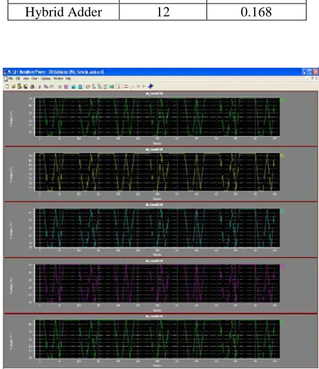
[image:3.612.85.303.462.628.2]Hybrid Adder 12 0.168
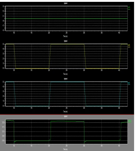
4. SIMULATION RESULTS
Figure 5: Waveform of Multiplexer Based Full adder
Figure 6: Waveform of Hybrid Full adder
5. CONCLUSION
The power performance characteristics of three different adders have been presented and the transistor count has been reduced. Compared to multiplexer based adder and conventional CMOS 28T adder, the hybrid adder exhibits better power performance. It is proved the logic restructuring
methods are effective in reducing power
consumption of the circuit, when the design of all architectures simulated using MOSIS 90nm Technology. The proposed approach resulted in low power consumption and high speed compared to the existing full adder architectures.
REFRENCES:
[1] S.Shah, A.J.Al-Khalili, and D.Al-Khalili, Comparison of 32-bit multipliers for various performance measures. Proceedingsof the
12th International Conference on
Microelectronics (2000), pp.75–80.
[2] Wang Q., Vrudhula S.B.K., “Multi-level logic optimization for low power using local logic transformations,” Computer-Aided Design,
1996. ICCAD-96., 1996 IEEE/ACM
International Conference on 10-14 Nov. 1996 Page(s):270 – 277
[3]Dhireesha Kudithipudi and Eugene John, Implementation of Low Power Digital Multipliers Using 10 Transistor Adder Blocks, Laboratory for Low Power Design, Department of Electrical and Computer Engineering, University of Texas at San Antonio, San Antonio, TX 78249, USA [4] Anantha P. Chandrakasan, Samuel Sheng, and
Robert W. Brodersen, Fellow, IEEE,
Low-Power CMOS Digital Design IEEE
JOURNAL OF SOLID-STATE CIRCUITS. VOL 27, NO 4. APRIL 1992.
[5] A. R. Fridi, “Partial multiplication: A low-power approach for parallel multiplier,” ECE729 Course Project, Dept. Electrical and Computer Eng., Univ. Waterloo, Apr. 1994. [6] R. V. Menon, S. Chennupati, N. K. Samala, D.
Radhakrishnan and B. Izadi, “Power
Optimized Combinational Logic Design,”
Proceedings of the International Conference on Embedded Systems and Applications, pp.
223 - 227, June 2003.
[7] J. J. F. Cavanagh, Computer Science Series:
Digital Computer Arithmatic. New York:
[image:4.612.79.298.433.679.2][8] A. Bellaouar and M. I. Elmasry, Low-Power
Digital VLSI Design Circuits and Systems.
Boston: Kluwer, 1995.
[9]J.Murugabharathi,M.Kalaiyarasi,Anusuyadevi, S.Kaliaivani, “Systematic Analysis on Power
Consumption in Conventional CMOS,
Multiplexer Based and Hybrid Adder” IOSR Journal of Electronics and Communication Engineering (IOSR-JECE) e-ISSN: 2278-2834, p-ISSN: 2278-8735. Volume 4, Issue 6 (Jan. - Feb. 2013), PP 89-93
[10] Y. Sasaki et al., “Pass transistor based gate array architecture,” in 1995 Symp. VLSI
Circuits, Dig. Tech. Papers, June 1995, pp.
123–124
[11] S. Devadas, S. Malik, “A Survey of Optimization Techniques Targeting Low Power VLSI Circuits,” Annual ACM IEEE Design Automation Conference, Proceedings of the 32nd ACM/IEEE conference on Design automation, San Francisco, California, United States, pp. 242 – 247, 1995
[12] Shih-Chieh Chang, Marek-Sadowska M, “Perturb And Simplify: Multi-level Boolean
Network Optimizer,” Computer-Aided
Design, 1994., IEEE/ACM International
Conference on November 6-10, 1994
Page(s):2 - 5