2018 International Conference on Computer, Communications and Mechatronics Engineering (CCME 2018) ISBN: 978-1-60595-611-4
Memristor Based Quantization Circuit Design for ADCs
Hai-jun LIU
1,*, Yue-wei HOU
1,2and Zhi-wei LI
11
College of Electronic Science, National University of Defense Technology, Changsha, P. R. China
2
31002 PLA troops, P. R. China
*Corresponding author
Keywords: Memristor, SPICE model, Quantization circuit.
Abstract. As the fourth fundamental circuit element, memristor will introduce great change to the conventional electronic circuits. Quantization circuit of ADC (Analog to Digital Converter) is one of the promising circuits applications that can be improved by memristors. In this manuscript, a parallel memristors quantization circuit design is proposed. The circuit with such implementation scheme is able to achieve high rate and high precision quantization conversion. Compared with other memristor based quantization circuit, it shows good performance in power dissipation and circuit size.
Introduction
Since the ADC (Analog to Digital Converter) is the main block in mixed signal applications, the design requirement for a low power, high speed and wide bandwidth ADC has increased tremendously, which becomes a bottleneck in data processing applications. And the performance of the quantization circuit mostly determines the performance of the ADC. Because the conversion rate, accuracy, and power consumption of the ADC are mainly determined by the quantization circuit part. At present, there is variety of quantization circuits with different CMOS circuit based architecture. The most widely utilized architectures include flash (parallel) ADCs, folding/interpolation ADCs and pipeline ADCs [1]. The fully parallel structure is characterized by high speed, but the resolution is difficult to increase and the power consumption is large. The folding/interpolation type has high resolution, low power consumption, but low speed and difficulty in further improvement. And the speed and resolution of the pipeline structure are relatively balanced, and have almost reached the theoretical upper limits. So it is imperative to study new quantitative circuit architectures based on some emerging devices.
Recently, memristors considered as a new fundamental two terminal circuit devices [2, 3], exhibit the expected advantages in high-density integration, low power consumption, and high-speed read and write [4]. Besides the crossbar architecture of memristor integration can significantly increase memory density while reducing power consumption. It should be highlighted that memristor has been highly considered to be one of the promising candidate for implementation of next generation non-volatile memory, which thus could advance Moore’s Law beyond the present silicon roadmap horizons. Moreover, memristive devices naturally combine the logic, storage and computing function together, which have a wide range of applications, covering almost all existing electronic circuits, and is constantly expanding its application fields [5-7].
Quantization Circuit Design with Memristors
Existing Memristor-based ADC Design
threshold, the memristor is activated and the state transitions. The voltage controlled memristor can be described by the following formula:
IM = [M (x, VM, t)]-1VM (1)
dx/dt = f (x, VM, t) (2)
Where IM is the current through the memristor and VM is the voltage across the terminals. M is the
memristance value, x is the internal state variable, and f is the dynamic function of the device. Assuming that the threshold voltage of the memristor is Vth, when |VM |>Vth the M value will be
changed. RON and ROFF are low resistance state and high resistance state, respectively, and the
corresponding logic values are 1 and 0.
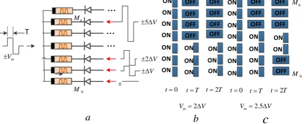
The published memristor-based ADC circuit and coding scheme are shown in Fig. 1. All the state of memristors in the same column are initially set to "on" (low resistance configuration). A synchronized pulse signal is applied to the two terminals of the memristor. The pulse width is T, and T is the shortest time that can guarantee changing the state of the memristor when the voltage exceeds the threshold. The amplitude of left pulse is Vin which is the pulse for the input signal sampling. The
amplitude of pulse on the right side is i∆V, i=0, 1, ..., N-1. In order to avoid an error when the input voltage is close to the threshold, let ∆V=4/3Vth. The pulse signals on both sides are inverted and
synchronously loaded on this series of memristors. Since the voltage difference across the memristor is greater than Vth, the memristor will transition from the "on" state to the "off" state. It can be seen
that when the first positive pulse acts on the memristor, all memristors with i>(Vin+Vth)/∆V are set to
the "off" state (the high resistance state). Since the diode at the right end, which only allows the forward current to pass, the latter negative pulse sets the memristor i<(Vin-Vth)/∆V to the "off" state,
i.e. avoiding the memristor that has been converted to the "off" state changing back to "on" state. When the pulse signal is applied, only one or two adjacent memristors are in an "on" state. When Vin is
close to an integer multiple of ∆V, there is a memristor in the "on" state, and when Vin is close to
(j+0.5) ∆V, where j is an integer, two memristors are "on" status. Figure 1 b and c show the main steps of the two conversion results.
T
…
… …
in
V
5 V
6 M
2 V
V
OFF ON
ON
ON
ON
ON
ON
ON OFF OFF
OFF OFF
OFF
OFF OFF
OFF
OFF
OFF OFF
OFF
OFF
OFF
OFF
ON ON
ON
ON ON ON
ON
ON
ON
ON
ON ON
ON
ON ON
ON
ON ON
ON
0
t tT t2T t0 tT t2T
2 in
V V Vin2.5V a
6 M
0 M
0 M
b c
[image:2.595.152.459.479.604.2]0
Figure 1. a. Existing memristor-based ADC design. b. The main steps of only one memristor in the "on" state after conversion. c. The main steps of having only one memristor in the "on" state after conversion.
Too much time cost in the read operation limits the conversion speed of the ADC and there is much room for improvement.
Improvement of ADC Design Based on Memristor
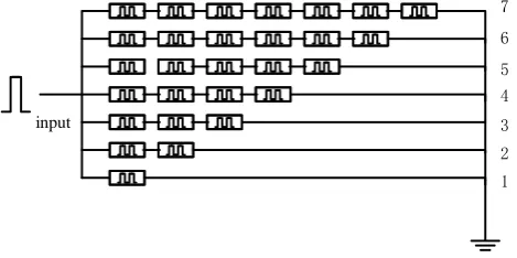
In this paper, a new quantization circuit based on memristor is designed for ADCs, as shown in Figure 2, which is an upper triangular resistance matrix formed by memristors. The i-th row has i memristors, and the memristors in each row are connected in series. The lines are connected in parallel, the left terminal is connected to the input signal, and the right terminal is grounded.
Initially, all memristors are "on" states. The input terminal applies a pulse signal with a width of ∆T, where ∆T is the minimum time for pulse changing the memristor’s state when the voltage Vin exceeds
the switching threshold value Vth. Since each memristor is in series relationship, the whole applied
voltage is divided by each other, the voltage amplitude of each memristor in the i-th row is shrinked to
Vin/i. When Vin>i*Vth, each memristor of the row number less than i is switched from the "on" state to
the "off" state, and the input pulse is quantized as iVth, and Vth is the minimum quantization unit.
input
[image:3.595.177.412.281.398.2]7 6 5 4 3 2 1
Figure 2. New design of Analog-to-Digital Converter Module Based on Memristor.
Lets’ take a 3-bit ADCs as an example to illustrate the design of this article. When the system has a input signal Vin, which equals 2.3Vth. Since 2.3Vth>2Vth, one memristor in the first row and two
memristors in the second row are converted to the "off" state, and the memristors on the row from line 3 to line 7 remain "on". That is, the input is quantized to 2Vth, and Vth is the quantized minimum unit
∆V. The high resistance state of the memristor indicates a logic value of ‘1’, and the low resistance state indicates a logic value of ‘0’. Finally, the quantization code stored in the memristors is 000011. The quantization coding scheme is shown in the following table:
Table 1. The proposed quantization coding scheme.
The amplitude of input signal The coding result 0 ≤ Vin < ∆V 0000000 ∆V ≤ Vin < 2∆V 0000001 2∆V ≤ Vin < 3∆V 0000011 3∆V ≤ Vin < 4∆V 0000111
… ...
Since the half of the converted memristor matrix is in the "on" state and the other half is in the "off" state, the order is arranged, so the strategy of folding the half can be used when reading the quantized result. Since the states of the individual memristors on each line are the same, each row only needs to read the state of one memristor. i.e. The n-bit ADCs module has a (2n-1-1) line, and first reads the state of the last memristor of the 2n-2th row, if it is the "on" state, Then read the last line of the (2n-2-2n-3) line; if it is "off state, read the second (2n-2+2n-3) the state of the row. By analogy, until an i-th behavior is "off" and its neighboring behavior is "on", the quantized result can be judged as iVth. Theoretically, for
Similarly, taking the above 3-bit ADC as an example again, when a signal Vin having a size of
2.3Vth is input to the left end of the system, the step of reading the quantized state is further explained,
which further explains the reading strategy. First read the last memristor on line 4 and find that its status is "on". Then read the last memristor on line 2 and find that its status is "off". Then read the last memristor on line 3 and find that its status is "on". Therefore, after three reading operations, it can be judged that the quantization result is 2Vth.
Simulation and Disscussion
The software used in this simulation was OrCAD Capture CIS, using the Spice simulation tool. The 3-bit quantization circuit in Figure 2 was constructed using the threshold memristor model. In this model, the equation (1) and (2) would be rewrite as:
IM = [M (x, VM)]-1VM (3)
dx/dt = {βVM+0.5(α-β)[|VM+Vth|-|VM-Vth|]}[θ(VM)θ(ROFF-x)+θ(-VM)θ(x-RON)] (4)
where Vth is threshold voltage, ROFF and RON are the high resistance and low resistance of memristor,
respectively. α and β are the fitting variable. Here the memristor simulation parameters are: RON=1000, ROFF=6K and the threshold voltage is Vset to 0.1V.
The simulation schematic is as follows:
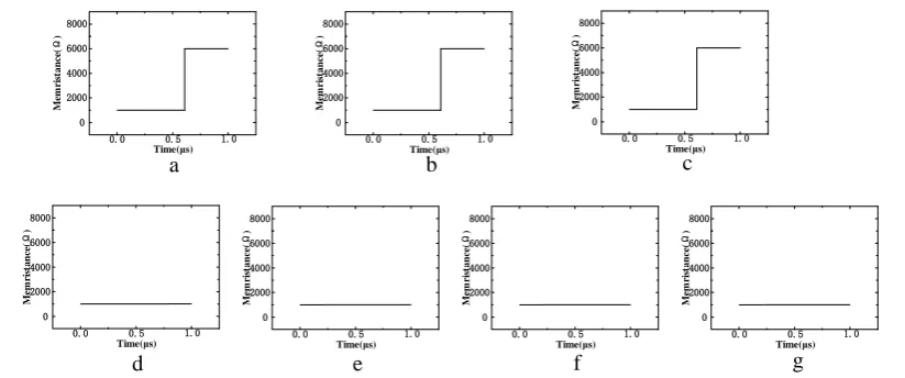
Set the input signal to 3Vth, and the output result is as shown in the figure below. The last memristor
in the first, second, and third rows becomes high resistance, and the last memristor in the remaining rows is in a low resistance state. The simulation result is shown in Figure 3.
0 2000 4000 6000 8000
0.0 0.5 1.0
Time(μs)
M
em
ri
st
an
ce
(
Ω
)
0 2000 4000 6000 8000
0.0 0.5 1.0
Time(μs)
M
em
ri
st
an
ce
(
Ω
)
0 2000 4000 6000 8000
0.0 0.5 1.0
Time(μs)
M
em
ri
st
an
ce
(
Ω
)
1.0 0
2000 4000 6000 8000
0.0 0.5
Time(μs)
M
em
ri
st
an
ce
(
Ω
)
1.0 0
2000 4000 6000 8000
0.0 0.5
Time(μs)
M
em
ri
st
an
ce
(
Ω
)
1.0 0
2000 4000 6000 8000
0.0 0.5
Time(μs)
M
em
ri
st
an
ce
(
Ω
)
1.0 0
2000 4000 6000 8000
0.0 0.5
Time(μs)
M
em
ri
st
an
ce
(
Ω
)
a b c
[image:4.595.95.507.392.564.2]d e f g
Figure 3. a~g is the resistance of the last memristor in the 1st row to the 7th row when the voltage is 0.3V.
Another test bench is to set the input signal 4.9Vth. The last memristor on the 1st, 2nd, 3rd, and 4th
0 2000 4000 6000 8000
0.0 0.5 1.0
Time(μs) M em ri st an ce ( Ω ) 0 2000 4000 6000 8000
0.0 0.5 1.0
Time(μs) M em ri st an ce ( Ω ) 0 2000 4000 6000 8000
0.0 0.5 1.0
Time(μs) M em ri st an ce ( Ω ) 1.0 0 2000 4000 6000 8000 0.0 0.5 Time(μs) M em ri st an ce ( Ω ) 1.0 0 2000 4000 6000 8000 0.0 0.5 Time(μs) M em ri st an ce ( Ω ) 1.0 0 2000 4000 6000 8000 0.0 0.5 Time(μs) M em ri st an ce ( Ω )
a b c
d e f g
0 2000 4000 6000 8000
0.0 0.5 1.0
[image:5.595.109.498.66.237.2]Time(μs) M em ri st an ce ( Ω )
Figure 4. a~g is the resistance of the last memristor in the 1st row to the 7th row when the voltage is 0.49V.
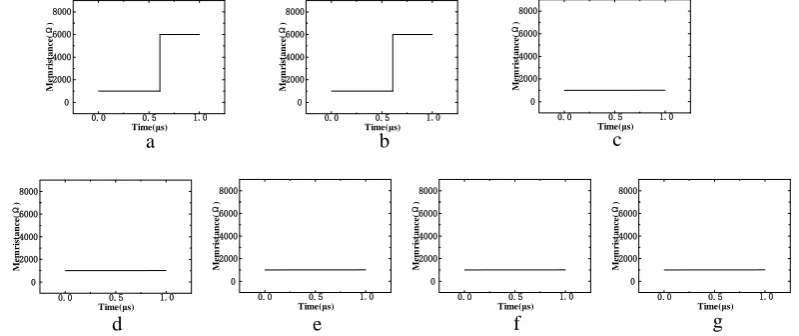
Then the final test bench is to set the input signal 2.3Vth. The last memristor on the 1st, 2nd, 3rd,
and 4th lines becomes high resistance, and the last memristor remains unchanged in 3 lines. The simulation result is shown in Figure 5.
0 2000 4000 6000 8000
0.0 0.5 1.0
Time(μs) M em ri st an ce ( Ω ) 0 2000 4000 6000 8000
0.0 0.5 1.0
Time(μs) M em ri st an ce ( Ω ) 1.0 0 2000 4000 6000 8000 0.0 0.5 Time(μs) M em ri st an ce ( Ω ) 1.0 0 2000 4000 6000 8000 0.0 0.5 Time(μs) M em ri st an ce ( Ω ) 1.0 0 2000 4000 6000 8000 0.0 0.5 Time(μs) M em ri st an ce ( Ω )
a b c
d e f g
1.0 0 2000 4000 6000 8000 0.0 0.5 Time(μs) M em ri st an ce ( Ω ) 1.0 0 2000 4000 6000 8000 0.0 0.5 Time(μs) M em ri st an ce ( Ω )
Figure 5. a~g is the resistance of the last memristor in the 1st row to the 7th row when the voltage is 0.23V.
All the simulation results show that it is feasible to construct an analog-to-digital conversion module and quantize the analog input signal into three state digital signals using a pure memristor network. According to the same circuit expansion and promotion, it is also feasible to construct a multi-bit analog-to-digital conversion circuit in principle. The quantized results are relatively stable and can be stored directly in the memristor. The conversion time is faster, which is the shortest time to convert the on and off states after the input exceeds the threshold voltage.
Summary
In this paper, a new quantization circuit based on memristor is designed for ADCs. Compared with the existing memristor-based ADC design, the power consumption is lower, the circuit is easier to implement, and the conversion speed is faster.
Acknowledgement
[image:5.595.99.499.307.475.2]References
[1] J V Patel, H Bhatt, Performance Evaluation of Different Types Of Analog To Digital, Converter Architecture. Esrsa Publications (2012).
[2] L. Chua, Memristor-The missing circuit element. IEEE Trans. Circuit Theory, (1971) 507-519.
[3] D. B. Strukov, G. S. Snider, D. R. Stewart, R. S. Williams. The missing memristor found, Nature, (2008) 80-83.
[4] J. J. Yang, D. B. Strukov, D. R. Stewart, Memristive devices for computing, Nature Nanotechnology, (2012) 13-24.
[5] Yu S. Neuro-Inspired Computing with Emerging Nonvolatile Memory, P. IEEE. (2018) 1–26.
[6] S. Kvatinsky, Memristor-based Logic Circuit Design, IEEE/ACRC Workshop on Memristors and Resistive Memory: Devices and Applications in Computer Architecture and Brain-Inspired Systems (2012).