Techniques for Low Power and Area Optimized VLSI
Testing using Novel Scan Flip-Flop
R. Jayagowri
Associate Professor,
Department of Electronics and Communication Engineering BMS college of Engineering, Bangalore
ABSTRACT
Power consumption of any circuit is high during test mode than its normal mode of functioning. Different techniques are proposed to reduce the test power. This paper presents the consolidated research work carried to reduce the test power. Usually the power dissipation is due to the sequential and combinational elements presents in the circuit. In this paper we proposed different methodologies and they are at cell level optimization to reduce test power. The structure of the scan flip-flop is modified to reduce the power due to sequential elements and gating techniques are proposed to reduce power duo to combinational elements. The proposed methodologies are implemented on the different ISCAS benchmark circuit and the experimental results were observed. These experimental results showed that our proposed methods reduced the switching power by 44.58-61.97%including the proposed gating technique, area by 30-45% and the test time by 50%.
General Terms
VLSI Testing, cell level optimization, Scan flip-flop modification.
Keywords
Scan flip-flop, Low power test, Shift cycle, Capture cycle
1.
INTRODUCTION
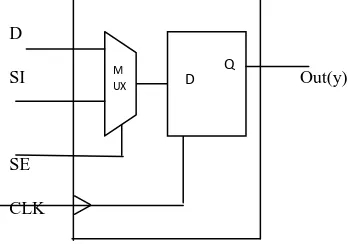
[image:1.595.79.254.608.730.2]Testing of any chip is mandatory to guarantee its functionality after the manufacturing Process. Based on type of the circuit, different testing techniques were proposed. Scan based testing is one of the popular testing technique for digital circuits [1]. During the logic synthesis phase of ASIC design the classical D- flip-flop is replaced by the scan flip-flop as a design for testability. The logic diagram of scan flip-flop is as shown in figure.1 usually the scan flip-flop is the combination of multiplexer and a D-flip-flop. These scan flip-flops are connected as a shift register to pass the test vectors into the circuit. [2].
Fig 1: Block diagram of Scan flop
Testing cycle includes sequence of three different cycles as shift-in, capture and shift-out. During shift-in and shift-out cycles the circuit remains in test mode and during capture cycle the circuit remains in normal mode. The power consumption during shift cycle is directly proportional to the switching activity of the number of components in the circuit due to the serial shifting of test vectors. Zorian showed that Power dissipation during test mode of an IC is significantly higher than during normal mode [3].
Different techniques are proposed to reduce the test power during both shift cycle and capture cycle. Software based method of reducing test power during shift cycle proposed by Dobholkar [4] where test vectors are reordered such that to reduce the number of transition in the circuit by 10% - 14%. Kajihara [5] proposed the software based method to reduce the switching activity in the circuit by filling the don‟t care value with the value of adjacent on the left. This method reduces the switching activity by 36% - 47%. Preferred fill is the software based power reduction method proposed by Ramersaro in [6] to reduce the switching activity of the circuit during capture cycle. There are few hardware based methods of reducing test power. Gerstendorfer [7] proposed a method of adding NOR gate with the scan cell to hold the constant output value in combinational circuit during scanning. Swarup Bhunia [8] proposed a technique of inserting extra supply gating transistor in the supply to ground path for the first-level gates at the outputs of the scan flip-flop. This method showed improvement of 62% in area overhead, 101% in power overhead and 94% in delay overhead. Amit Mishra [9] proposed a modified scan flip-flop for low power testing in which the flip-flop disables the slave latch during scan and uses an alternate low cost dynamic latch. There are different latches and flipflops with many different techniques are proposed in[14-16] to reduce power and delay during testing. This paper presents the consolidated research work for power optimized testing of VLSI chips. The rest of the paper is organized as follows. Section-2 describes the different approaches in our work. Section-3 presents the experimental results and detailed discussion about it. The conclusion is given in section-4.
2.
PROPOSED TECHNIQUES
The major objective of our work is to reduce the power consumption of dedicated circuit for DFT in the design. This objective leads us to frame the problem as a modification on the scan flip-flop used for the purpose of testing. To satisfy the objective and solve the problem, sequence of approaches were followed in our experiment and they are presented in this section.
D
SI Out(y)
SE CLK
op M
UX
2.1
Approach1
The first approach of our experiment is using a double edge triggered (DET) flip-flop which is constructed using a positive edge triggered and a negative edge triggered flip-flop s with a multiplexer as a selector. This architecture preceded by a multiplexer used as a DET scan flip-flop. It has 4 latches and 2 multiplexers as in the Fig.2. When the clk=0 the negative latch (L1) of the positive edge triggered flipflop and the negative latch (L4) of negative edge-triggered flipflop is transparent. The latch (L4) is responsible for the output change of negative edge triggered flip flop. The selector (or) the multiplexer selects the output of the latch (L4), which is needed to be transferred to the output (Y). Similarly when clk=1 the positive latch (L2) of the negative edge triggered flipflop and positive latch (L3) of the positive edge triggered flipflop are transparent .The multiplexer selects the output of L3 to Y. When clk=1 the value of L1 is need to be passed out through the latch (L3) to Y and the latch(L4) left idle until the „0‟ logic clock arrives. Similarly during clk=0 the output of latch (L2) is need to be passed to Y through latch (L4) and the latch (L2) left idle. This type of scan flip-flops captures the required n-bit data by n/2 clock cycles where the classical scan flip-flops needs n clock cycles for the same. So, it reduces the clock switching power of the flip-flop as shown in equation1
Pclk = V2dd . fclk [(Cclk+Cclkp) + DR. Cdap] (1) Even though double edge triggered flip-flop is able to capture the data fast with less power consumption, this technique is not so popular because it occupies double the amount of area when compared to the single edge triggered flip-flop [10]. This sentence is the original motivation for our work. To overcome this problem the pipelined double edge triggered (PDET) scan flip-flop has been proposed. The classical double edge triggered scan flip-flop has two multiplexer and 4 latches. The proposed PDET scan flip-flop has only two latches and two multiplexer cells as shown in Fig.3.The right hand sided multiplexer in the Fig.3 will act both like a selector switch and also as a latch. This is achieved by bringing a pipelined architecture in the latches of double edge-triggered flip flop as shown in Fig.2 the blocks that performs the Pipelined architecture is denoted by the dotted line. To reduce the area of the flip-flop, the latches L3, L4 and the selector are overlapped to generate the pipelined double edge triggered flip flop.
D
Si
Clk
Se Out(Y)
[image:2.595.315.538.76.227.2]Clk
Fig 2: Block diagram of DET scan flip-flop
D
Si Out(Y) Se
Clk
Fig 3: PDET scan flip-flop
The results of these experiments are discussed in section-3.
2.2
Approach2
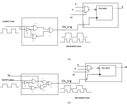
In approach-2 a scan flip-flop is proposed which is constructed by only one positive latch. This single positive latch itself made to work as a flip-flop which can capture the change in data only during the edges of the clock pulse. This is achieved by generating a clock trigger signal from the system clock pulse. The generated clock trigger signal has very narrow ON time which exactly coincides with the edges of the system clock to capture the data either at the positive or negative edges of the system clock. The same flip-flop can be made to capture the data during both positive and negative edges of clock then it works like a double edge triggered (DET) flip-flop. The OLDET flip-flop can be introduced into testing as a scan flip-flop just by combining it with the multiplexer. The block diagram of one latch-double edge triggered (OLDET) scan flip-flop is shown in Fig.4 (a). The total number of cells and the switching nodes of the cells in the OLDET scan flip-flop is less when compared to the other type of scan flip-flops. This leads for the reduction in total switching and leakage power.
During the shift-in and shift-out cycle of testing the circuit works in test mode where the entire scanflop works as a shift register and it is independent of the combo cloud present in the circuit and it can work comfortably with half a clock cycle. But, during capture cycle the circuit works in the data mode. It is necessary that combo cloud should evaluate the vector values from the flip-flop and the output from combo is captured again by the flip-flop in the RTL design. The entire evaluation of combo should happen in half a cycle, if the scan flip-flop is a double edge triggered scan flip-flop. It is advantageous in one way as a fast system but, another way it may lead for more number of timing issues. To overcome this problem the same scan flip-flop is modified as dual mode double edge triggered (DMOLDET) scan flip-flop just by modifying the clock trigger generator circuit. The circuit diagram of modified clock trigger generator is shown in Figure.4 (b).
In the proposed modified dual mode one latch double edge triggered (DMOLDET) scan flip-flop is made to work both as a positive edge triggered flip-flop in one mode and double edge triggered flip-flop in another mode. The and-gate (A1) is responsible for generating the pulse with a narrow on time as a output of clock generator, during the positive edge of the system clock. Similarly Nor-gate (A2) is responsible for the generating pulse with narrow ON time during the negative edge of the system clock. The inverter (A6) in the circuit is a slow gate when compared to other gates. This gate is responsible for a narrow ON time of the generated clock
(-) ve
latch
L1
1
0 0
1
1
(+) ve
latch
L2
(-)ve latch
L1
(+)ve latch
L2
(+)ve latch
L3
(-)ve latch
L4
1
0 0
1
1
pulse. During ON time of the generated clock pulse the latch in Flip-flop captures the change in the data. The and-gate (A4) in the circuit helps the entire flip-flop to work in the dual mode. During the test mode scan enable (se = 1) which allows the clock trigger generator to generate narrow positive pulse (ON time) during both positive and negative edges of the system clock. So, the flip-flop works as a double edge triggered flip-flop during shift-in and shift-out cycle of testing. During the capture cycle the circuit enters into the data mode with the values of scan enable (se= 0) which stops generating the positive narrow pulse during the negative edge of the system clock. It allows the circuit to generate the narrow pulse only during the positive edge of the system clock. So, the DMOLDET scan flip-flop works as a single edge (only positive) triggered flip-flop in data mode. It solves
the timing problem and reduces the unnecessary partitioning of the circuit required to satisfy the timing issue of circuit during its functional mode.
The proposed DMOLDET scan flip-flop is efficient enough to reduce the power during testing like OLDET scan flip-flop because, the total number of cells and the switching nodes of the cells in the DMOLDET scan flip-flop is also less when compared to the other type of scan flip-flops. The DMOLDET scan flip-flop also requires only n/2 number of cycles of system clock to shift-in or shift-out n-vectors into the „n‟ number of flops of scan chain. Because these scan flip-flops can captures two data per system clock cycle. So, this scan flip-flop can reduce the switching power, leakage power and required silicon area for scan flip-flop in the design. It can also increase the speed of testing.
(a)
Generated clock (b)
Fig:4 (a) Block diagram of one latch Double Edge Triggered Scan flip-flop (b) Block diagram of Dual Mode one latch Double Edge Triggered Scan flip-flop
[image:3.595.55.500.233.596.2]2.3
Approach3
Fig :5 Switch level circuit of the proposed scan flip-flop(excluding the clock driver circuit)
In order to apply the test vectors into the circuit the scan flip-flops are stitched as a scan chain. When output of clock driver circuit is high then the data is latched into the scan flip- flops. Since all the latches in the DMOLDET scan flip-flop is positive level triggered latches it is wide open for the data from first latch to till the output of the last flip-flop in the scan chain. To overcome this problem a simple dynamic latch circuit is connected with the output of every proposed DMOLDET scan flip-flop. If the clock driver circuit output is in logic low, the data is stored in the dynamic latch until the next narrow positive pulse arrives in the scan flip-flop. The switch level circuit diagram of the proposed scan flip-flop is shown in Fig. 5.
Pos latch D
Q Si
Se
Clk_trig
A3 A2
A1
A5 System clock
Generated clock
Se
A3
A2 A1
Clk_trig
System clockA4 A5 A6
Pos latch D
Q Si
Se
clk-trigout
clk-trig_out
q
D
[image:3.595.63.267.639.738.2]2.4
Approach4
Usually the RTL circuit is a combination of registers and combinational circuit cloud. All the above approaches are concentrated to reduce the power consumption of the registers. In this approach we propose two gating methods for our proposed DMOLDET scan flip-flops to reduce the combinational circuit switching power[13]. They are,
Technique1: Using the gate at the output of the dynamic latch, Technique2: Using the gate at the output of the static latch.
Technique1: The PMOS pass transistor is connected between the output of the dynamic latch and the combinational cloud. The gate of the PMOS pass transistor is connected with the „se‟ signal. During the test mode and the PMOS will be in OFF condition it does not allow the data to pass from flip-flop to the combinational circuit. During the functional mode the transistor allows the data to pass from flip-flop to the combinational circuit. Even though PMOS Pass transistor face the threshold drop while passing the logic value of „0‟ it can be easily compensated by the CMOS circuit in the combo cloud. The circuit arrangement for the gated DMOLDET scan
(a)
(b)
Fig:6 Switch level circuit diagram of the Gating technique (A) PMOS gated DMOLDET scan flip-flop (B) NMOS and NOR gated DMOLDET scan flip-flop
flip-flop is shown in Fig.6 (A). In this gating method, the dynamic latch inverter should be strong enough to drive the fan-out faced by it, due to the combinational circuit connected with it. To overcome this problem if we select the strong inverter it may lead for increase in power dissipation. It is observed as a drawback for the high fan-out circuits.
Technique2: The drawback of the above said technique has been overcome by further modifying the gating circuit as shown in Fig.6 (B). In this gating method the NMOS can be connected between the output of the static latch and the combinational circuit in the cloud. The gate terminal of NMOS is connected to the output of NOR gate (U1) and the NOR gate‟s two inputs are clk_trig and se. When both the inputs are at at logic ‟0‟ then the value retained in the static latch is passed to the combinational circuit. This helps to
select the weak inverter in dynamic latch because it need to drive only the multiplexer of the next scan flip-flop in the scan chain so it reduces the power dissipation due to gating circuit. But here the extra silicon area for the amount of NOR gate is need to be sacrificed only once for the entire design. The amount of extra silicon area required for this technique is less when compared to the other gating techniques.
2.5. Characterization of proposed flip-flop
Setup time: It is the time required for the input signal at the flip-flop to be valid before the incoming clock edge arrives. To measure the setup time of the proposed scan flip-flop the time gap between the falling edge of data input before the rising edge of clock to rising edge of the clock. To measure the setup time and the corresponding clk-q delay it isDynamic latch Static latch
si se D
q
clk-trig
clk-trig
Gating circuit
se
To combinational cloud
Q (to the
input terminal
si of next
scan flip-flop )
Dynamic latch Static latch
clk-trig
si se
D
clk-trig
Q (to the
input terminal
si of next
scan flip-flop )
Gating circuit
To
combinational
cloud
se
necessary to begin the data arriving much earlier than the clock rising input. The experiment carried out here the data began at 2ns earlier than the clock rising edge. The setup time is determined. by continuously reducing the time interval between falling edge of data and rising edge of clock. The experimentation is continued until the flop reaches the metastable state.
T setup = max (ts 0 ->1, ts 1 ->0) (2.1) Hold time: It is the time required for the input signal at the flip-flop to be stable after the rising edge of clock. To measure the hold time of the proposed scan flip-flop, the time gap between the falling edge of data input after rising edge of clock to the rising edge of the clock. To measure the hold time and the corresponding clk-q delay it is necessary to begin the data remains stable much later than the clock rising input. The experiment carried out here, the data began at 2ns difference between data falling and the clock rising edge. The hold time is determined by continuously reducing the time interval between falling edge of data and rising edge of clock. The experimentation is continued until the flip-flop reaches the metastable state. The metastable state of the scan flip-flop is observed in experimentation as an oscillation in the output. This is done for both data rising (0 -> 1) and data falling (1 -> 0).
T hold = max (th 0 ->1, th 1 ->0) (2.2)
3.
RESULTS AND DISSCUSSION
The proposed techniques are implemented into the different ISCAS benchmark circuits. These benchmark circuits are then simulated and synthesized to evaluate its performance after implementing the proposed techniques. The circuit functionality is verified using NCSIM of cadence tool and the simulated output of approach2 is shown in Fig.7. Production of narrow pulses in the clock driving circuit are clearly seen from the simulated output that the circuit functions in the test mode when se=1 and the narrow pulses are generated by the clock driver circuit both at the rising edge and falling edge of the system clock. Similarly when se=0 the circuit functions in the normal mode, the clock driver circuit generates the narrow pulse only at rising edge of the clock. The switch level circuits using both the gating techniques are implemented and simulated using cadence spectre with 180nm technology. The simulated output of first proposed gating technique and second proposed technique are shown in Fig. 8(A) and Fig. 8(B) respectively. Fig. 8 clearly shows that there is no switching takes place in the combinational circuit during the signal se at logic „1‟ and that is shown in the waveform as „from_combo‟ signal.
Fig:7 Simulated output of the DMOLDET scan flip-flop.
(a)
(b)
(c)
Fig: 8 Simulated output of the proposed DMOLDET scan flip-flop with dynamic latch and gating technique for combo at 100 MHz (A) at the output of dynamic latch (B) at the output of static latch (C) scan chain with 3 flip-flops
at test mode including gating technique
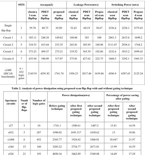
The area analysis of different techniques from the table.1 shows that the required area for the PDET scan flip-flop is slightly higher when compared to the classical scan flip-flop. In case of proposed scan flip-flop the required area of the scan flip-flop should be lesser when compared to the other scan flip-flops because each flip-flop contains only one latch. But, it is greater if a single proposed scan flip-flop is considered and it rapidly reduces the number of flip-flops increases in the scan chain. That is because the proposed scan flip-flop needs only one clock driver circuit for the different number of flip-flops.
The switching power dissipation and leakage power dissipation are compared for different techniques. It can be observed from the table.1 that there is reduction of switching power is achieved by PDET scan flip-flop but the leakage power is high compared to the classical flip-flop because of its total number of cells in the circuit. The significant amount of power reduction has been observed with the proposed technique. The reason for this power reduction is the total number of cells and the switching nodes of the cells in the DMOLDET scan flip-flop is also less when compared to the other type of scan flip-flops like OLDET scan flip-flop.
[image:6.595.64.533.210.710.2]Table 1 Comparison of different scan flip-flops
Table 2. Analysis of power dissipation using proposed scan flip-flop with and without gating technique
Specimen circuits
Numb er of flip-flops
Number of logic gates
Power dissipation(nws) Percentage of power saving after gating Before gating
technique
After first proposed gating technique
After second proposed
gating technique
After first proposed gating technique
After second proposed
gating technique
s27 3 10 1741.1 1500.61 1487.2 13.81 14.58
s832 5 287 1990.02 1691.517 1630.62 15 18.06
s1488 6 652 2365.77 1924.62 1846.01 18.647 21.97
s344 15 160 3203.22 2754.77 2671.81 13.99 16.59
s526 21 193 4050.16 3462.89 3349.88 14.49 17.29
To analyze the power saving of using gating techniques with the proposed scan flip-flop some of the ISCAS bench mark circuits taken as the specimen circuits. The switching power dissipation before and after gating technique is observed and
listed in Table2. The table shows the further reduction of power after gating technique when compared to before gating technique. With the usage of proposed scan flip-flop the improvement in terms of area for DFT in the circuit, Speed of testing and test power reduction have been achieved.
#FFS Area(µm2) Leakage Power(nws) Switching Power (nws) classica
l scan flipflop
PDET scan flipflop
proposed scan flipflop
classical scan flipflop
PDET scan flipflop
Propos ed scan flipflop
classical scan flipflop
PDET scan flipflop
Propose d scan flipflop
Single
flip-flop 1 59.70 80.73 65.89 52.43 60.19 38.67 2526.4 2236.1 1575.63 Circuit 1 3 185.11 248.18 149.62 160.06 183 100 2861.3 2615.6 1698.2 Circuit 2 5 310.53 415.64 233.35 265.81 305.95 160.98 3111.07 2936.4 1764.2 Circuit 3 6 373.23 499.37 275.21 319.52 365.39 192.86 3232.6 3015.2 1899.43 Circuits 4 7 435.94 580.09 317.07 375.81 427.62 222.75 3460.5 3292.1 1965.33
s1488 (ISCAS benchmark)
6 + 652 logic gates
The characteristics of the flip-flop are observed using the cadence tool. The characteristic curve which is observed during experimentation for setup time is shown in Fig.9 and for hold time is shown in Fig.10.
Fig:9 setup time Vs clock-to-q delay. Ts 0 ->1 = 0.2236ns, Ts 1 ->0 = 0.2235ns T setup = max (0.2236ns, 0.2235ns) = 0.2236ns
Fig:10 Hold time Vs clock-to-q delay. Th 0 ->1 = 0.14725ns, Th 1 ->0 = 0.14720ns T hold = max (0.14725ns, 0.14720ns) = 0.14725ns
4.
CONCLUSION
The proposed DMOLDET scan flip-flop reduces the power dissipation during shift cycles of the scan. This technique is suitable for any scan based testing circuit. The result shows that usage of the proposed scan flip-flop reduces the silicon area by 30% - 45%, the power dissipation by 25% - 35%. It doubles the testing speed. When compared to the scan flip-flop in [9], the proposed scan flip-flop shows 45% reduction in terms of required silicon area and double the amount of increase in terms of testing speed. This technique can be easily incorporated with other power reducing techniques. Our scan flip-flop output is gated as the method proposed in this paper to eliminate the unnecessary switching in combinational circuit during the scan. It further reduced the power dissipation in the ISCAS benchmark specimen circuits by 13.81-18.647% using the first proposed technique and by 14.58- 21.97% using the second proposed gating method. As a future work different power optimized techniques can be implemented on the DUT by substituting this scan flip-flop in the design.
5.
REFERENCES
[1] Vishwani D Agarwall, Michael „L‟ Bushnell, “Essentials of electronic testing for digital memory and mixed signal vlsi circuits, kluwar academic publisher, 2000 .
[2] Alfred.L.Crouch, “ Design-for-Test for Digital IC‟s and Embedded Core Systems”, Prentice Hall PTR,ISBN 0-13-084827-1,2000.
[3] Zorian, Y.,:A distributed BIST control scheme for complex VLSI devices. In.: IEEE VLSI test symposium, pp. 4-9.(1993)
[4] Dobholkar, V. et al.,:Techniques to minimize power dissipation in scan and combinational circuits during test application. In: IEEE Transactions on computer aided design, pp.1325-1333.Dec (1998)
[5] Kajihara, S. et al.,: Test vector modification for power reduction during scan testing. In: Proceedings VLSI test symposium, (2002)
[6] Ramersaro et al.,:Preferred Fill: A Scalable Method to Reduce Capture Power for Scan Based Designs. In: International Test Conference, pp.1-10. (2006)
[7] Gerstendorfer, S., Wunderlich, H. J.,:minimized power consumption for scan based BIST. In: proceeding International Test Conference, (1999)
[8] Swarup Bhunia, Hamid Mahmoodi, Dabjyothi Ghosh, saibal Mukhopadhyay, k.roy,: low power scan design using first level supply gating. In: IEEE transactions on VLSI system, vol 13, no 3, pp.384-395. (2005)
[9] Amit mishra, Nidhi sinha, Satdev, virendra singh, Sreejit chakravarthy, Adit.D. Singh,:Modified scan flip flop for low power testing. In: Proceedings 19th IEEE Asian Test Symposium, pp.367 – 370. (2010)
[10] Kiat-seng Yeo,samir.S Rafail,s Wangling croh, CMOS BICMOS VLSI- low voltage ,low power, Pearson education pvt.Ltd.2002.
[11] Jayagowri, R., Gurumurthy, K.S.,: Design and Implementation of Area and Power Optimised Novel ScanFlop. In: International Journal of VLSI design & Communication(VLSICS),Vol.2, no. 1, pp. 37-43.(2011) [12] Jayagowri, R., Gurumurthy, K.S.,: A Technique for Low
Power Testing of VLSI Chips. In: Proceedings of IEEE International Conference on Devices, Circuits and Systems,DOI:10.11.1109/ICDCSyst.2012.6188654, pp. 662-665.(2012).
[13] Jayagowri, R, Gurumurthy, K. S,: Implementation of Gating Technique with Modified Scan Flip-Flop for Low power Testing of VLSI Chips. Progress in VLSI Design and Test, DOI: 10.1007/978-3-642-31494-0_7, Proceedings of 16th International Test Symposium, VDAT 2012, LNCS Vol.7373, pp. 52-58(2012).
[14] Yang Lu, Lombardi, F, Pontarelli,S, Ottavi, M,: Design and Analysis of Single event Tolerant Slave Latches for Enhanced Scan Delay Testing. IEEE Transaction on Device and Material Reliability, Vol.1, Issue 14, pp. 333-343(2014).
[15] Hsing-Chung liang, Chang-Jung Ho,: Multifunction Controller for low-power multiple scan test of transition delay Faults, In: Proceeding of International Symposium on Next Generation Electronics, DOI: 10.1109/ISNE.2014.6839366, pp. 1-3(2014).