Structural and electronic properties of Li-intercalated graphene on SiC(0001)
Nuala M. Caffrey,1,*Leif I. Johansson,1Chao Xia,1Rickard Armiento,1Igor A. Abrikosov,1,2,3and Chariya Jacobi1 1Department of Physics, Chemistry and Biology (IFM), Link¨oping University, SE-581 83, Link¨oping, Sweden
2Materials Modeling and Development Laboratory, NUST “MISIS,” 119049 Moscow, Russia 3LACOMAS Laboratory, Tomsk State University, 634050, Tomsk, Russia
(Received 26 February 2016; published 16 May 2016)
We investigate the structural and electronic properties of Li-intercalated monolayer graphene on SiC(0001) using combined angle-resolved photoemission spectroscopy and first-principles density functional theory. Li intercalates at room temperature both at the interface between the buffer layer and SiC and between the two carbon layers. The graphene is stronglyn-doped due to charge transfer from the Li atoms and twoπbands are visible at the ¯Kpoint. After heating the sample to 300◦C, theseπbands become sharp and have a distinctly different dispersion to that of Bernal-stacked bilayer graphene. We suggest that the Li atoms intercalate between the two carbon layers with an ordered structure, similar to that of bulk LiC6. An AA stacking of these two layers becomes energetically favourable. Theπbands around the ¯Kpoint closely resemble the calculated band structure of a C6LiC6system, where the intercalated Li atoms impose a superpotential on the graphene electronic structure that opens gaps at the Dirac points of the twoπcones.
DOI:10.1103/PhysRevB.93.195421
I. INTRODUCTION
The epitaxial growth of graphene on SiC substrates is a viable and attractive way of producing large homogeneous monolayer samples suitable for electronic device applica-tions [1,2]. When grown on the Si terminated SiC(0001) surface, the first carbon buffer layer has a detrimental effect on the graphene charge carrier mobility and needs to be eliminated [3]. Intercalation of elements such as hydro-gen [4,5], gold [6], germanium [7], silicon [8,9], nitrogen [10], fluorine [11], oxygen [12], lithium [13–15], and sodium [16–18] have all been shown to decouple the buffer layer and transform it into a quasi-free-standing graphene layer with varying degrees of doping depending on the intercalant. The alkali metals induce a strongn-type doping when deposited on graphene samples. Potassium [19,20], rubidium, and cesium [21] remain on the surface after deposition and do not penetrate to the interface even after heating. Lithium [13–15] and sodium [16–18], on the other hand, intercalate readily at room temperature, decoupling the buffer layer. Increasing the temperature to 300◦C (100◦C) promotes the complete intercalation of Li (Na), while higher temperatures result in the deintercalation and desorption of the metal from the sample. Interest in Li-intercalated graphene was originally motivated by the possibility of using it to improve the capacity of Li-ion batteries. However, the structural degradation of the carbon layers after Li deposition renders this unlikely [14]. More recently, superconductivity was discovered to occur in Li decorated monolayer graphene on SiC(0001) at low temperatures [22,23]. Detailed studies of the structural and electronic properties of Li intercalated graphene will be required in order to determine the origin and mechanism of this behavior.
Low-energy electron microscopy (LEEM) imaging provide evidence that Li atoms form small islands on the graphene surface directly after deposition [14]. Over time, these islands
coalesce, shrink and eventually disappear; this process can be accelerated by annealing. Core level spectra, combined with angle-resolved photoemission spectroscopy (ARPES) data, show that Li intercalates both at the interface between the substrate and the buffer layer and between the carbon layers, with the result that multipleπ bands become visible [13,15]. A (√3×√3)R30◦ diffraction pattern was observed after Li deposition on monolayer graphene using low-energy electron diffraction measurements. This pattern did not appear when Li was deposited on a sample containing only the (6√3× 6√3)R30◦carbon buffer layer, suggesting that it is due to an ordered intercalated Li layer between the two graphene sheets. The decoupling of the buffer layer was also shown to occur when Li was deposited on samples with an initial coverage of only the buffer layer. In this case, a singleπ band becomes visible directly after Li deposition [14], which can only occur if the buffer layer has been decoupled.
Several recent investigations have attempted to elucidate the exact nature of the Li intercalation on both zero- and monolayer graphene and its temperature dependence. Bisti et al. determined that the Li atoms occupy the T4 site of the topmost SiC bilayer after they intercalate underneath the buffer layer, thereby decoupling it from the substrate [24]. Sugawara et al. deposited Li on bilayer graphene at 30 K and reported the appearance of a sharp (√3×√3)R30◦ diffraction pattern [25], but did not observe this pattern after the deposition of Li on monolayer graphene. They suggested Li intercalates between the top two adjacent carbon layers and takes the same well-ordered superstructure as in bulk C6Li. However, the band structure around the ¯K point for both Li-deposited monolayer and bilayer graphene contained only a singleπband (see Figs.2(e)and2(f)in Ref. [25]). This contrasts significantly with earlier findings [13–15] where at least twoπbands appear around the ¯Kpoint after Li deposition on monolayer graphene.
present and their dispersions. Directly after deposition, we show clearly the presence of multipleπ bands around the ¯K
point. After heating the sample to 300◦C, these bands become considerably sharper and their dispersions do not resemble that of Bernal stacked bilayer graphene [26,27]. To understand these observations, tight-binding and density functional theory band structure calculations were performed for Li intercalated free-standing bilayer graphene, as well as for Li-intercalated graphene systems that explicitly take the SiC(0001) surface into account.
Our combined experimental and theoretical results lead us to suggest the following: Directly after deposition, Li intercalates both underneath the buffer layer and between the two carbon layers. Heating the sample promotes the complete intercalation of the Li atoms to the interface, as well as the development of an ordered Li configuration between the two carbon layers. In the process, it becomes energetically more favorable for the carbon layers to become AA rather than Bernal-stacked. We show that theπbands visible around the ¯K
point closely resemble the band structure of a C6LiC6system as calculated with density functional theory. The periodic perturbation of the graphene electronic structure by the ordered Li layer induces “gaps” to open at the Dirac point of each of the
π cones. Tight-binding calculations show that the interlayer coupling is enhanced by the presence of the Li atoms beyond what is typical in clean bilayer graphene, and the impact of the enhanced coupling terms on the band dispersion is verified by ARPES spectra.
II. METHODOLOGY A. Experimental details
Monolayer graphene samples were grownin situonn-type wafers of 4H-SiC(0001) purchased from SiCrystal, which were specified to have a misorientation error within 0.05◦. ARPES measurements were performed using Beamline I4 on the MAX III ring at the MAX IV Laboratory, which is equipped with a spherical grating monochromator and a PHOIBOS 100 mm CCD analyzer from SPECS. The wide angular dispersion mode was selected, providing an acceptant angle of±14◦. Each ARPES spectrum was collected parallel to theA- ¯K-Adirection of the Brillouin zone of graphene [see Fig.1(j)], in steps of 0.25◦along the ¯- ¯K- ¯Mdirection, using photon energies of 33 and 70 eV. From this data, theπ-band structure along certain directions in the Brillouin zone can be determined, as well as the angular distribution pattern, Ei(kx, ky), at selected initial state energies. A Ta foil was used as a reference to determine the Fermi level.
Deposition of Li was performed during a five minute interval using a commercial alkali metal source (from SAES Getters) and with the sample at room temperature. Further details can be found in Refs. [13–15]. Subsequent heating was carried out for four minutes at each selected temperature.1The sample temperature was determined using optical pyrometers.
[image:2.608.313.558.65.379.2]1Two sets of data were collected from two different monolayer graphene samples. For the first sample, the heating was carried out in steps at 8 different temperatures from 150◦C to 450◦C, while for the second sample the temperature was raised directly from room
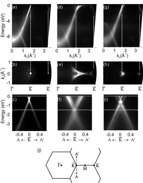
FIG. 1. Band dispersion recorded from monolayer graphene samples before [(a)–(c)] and after [(d)–(f)] Li deposition, and after heating to 300◦C [(g)–(i)]. The dashed lines are guides to the eye for illustrating the location of the first and second ¯Kpoints or an initial state energy of 0 eV and−1.4 eV. The Fermi energy is located at 0 eV. (j) The 2D Brillouin zone of graphene showing the ¯, ¯M, and
¯
Khigh-symmetry points. TheAandAdirections are also shown.
ARPES measurements were taken after the sample had cooled to room temperature. The Si 2p and Li 1score level spectra were recorded before and after deposition, as well as after heating, and their peak areas were extracted. After Li deposition a Li 1s/Si 2p peak area ratio of around 1.6 was obtained which decreased to around 0.5 after heating to 300◦C. Using a simple layer attenuation model,2 these ratios suggest the presence of three layers of Li in the surface region after Li deposition; one layer at the interface, one in
temperature to 300◦C. The band structure data obtained for both samples, both after Li deposition and after heating at 300◦C, were essentially identical.
between the carbon layers and one on top of the graphene. After heating at 300◦C the ratio suggests that only the Li layers at the interface and in between the carbon layers remain while the Li on top of graphene has disappeared, in agreement with earlier LEEM/PEEM results [14]. As the core level data showed the same features and changes upon heating as reported earlier [13], no core level data are included below.
B. Computational details
Density functional theory calculations were performed using VASP-5.3 [28–30]. The Perdew-Burke-Ernzerhof (PBE) [31] parametrization of the generalized gradient ap-proximation (GGA) was employed. The plane-wave basis set was converged using an 800 eV energy cutoff. Structural relaxations of the C6LiC6 cell were carried out using a 9×9×1 k-point Monkhorst-Pack mesh [32] to sample the Brillouin zone. A 24×24×1 mesh was used to determine the total energies. The Tkatchenko-Scheffler method was used to describe van der Waals interactions [33]. The free-standing bilayer structures were optimized until all residual forces were less than 0.001 eV ˚A−1.
The SiC(0001) substrate was modelled using an asymmetric slab consisting of six bilayers of SiC(0001), arranged in the ABCACB stacking associated with the 6H polytype. A bulk termination was assumed. The GGA calculated lattice constant of bulk SiC is 3.09 ˚A, in good agreement with the experimental value of 3.08 ˚A. A vacuum layer of at least 15 ˚A was included in the direction normal to the surface to ensure no spurious interactions between repeating slabs and the dipole correction was applied where appropriate. The dangling C bonds on the SiC(000¯1) surface were passivated with H atoms. The positions of the top two bilayers of SiC(0001), as well as the H-terminating atoms, the Li atoms, and all carbon layers, were optimized until all residual forces were less than 0.01 eV ˚A−1. The remaining atoms were held fixed at their bulk positions. The (6√3×6√3)R30◦surface reconstruction [34–37] of the buffer layer on SiC(0001) was modelled using the simplified (√3×√3)R30◦cell which corresponds to a 2×2 graphene cell. Such an approximation was shown to be adequate to correctly describe the interaction between the SiC(0001) surface and the carbon layers [38].
III. RESULTS
A. Experimental ARPES spectra
The band structure obtained from the as-grown monolayer graphene sample, along the ¯- ¯K- ¯Mdirection of the Brillouin zone of graphene, is displayed in Fig.1(a). The contribution from the π band dominates, with branches visible at both the first and second ¯K point. The photoelectron angular distribution pattern, Ei(kx,ky), obtained at the Fermi energy is shown in Fig. 1(b). The image has been overexposed to show the presence of six replica π cones surrounding the Dirac cone at the first ¯K point, as well as the presence of the Dirac cone at the second ¯K point. The Fermi surface at the second ¯K point appears, when further exposing the image, as a segment of a circle [39,40]; it is a mirror image of the one at the first ¯K point. The lower intensity obtained around the second ¯K point is attributed to photoelectron
matrix effects [39,41]. The π-band structure obtained along the A- ¯K-A direction around the first ¯K point is shown in Fig.1(c). A single, linearly dispersingπ band is visible with the Dirac point located approximately 0.45 eV below the Fermi level. Taken together, the ARPES spectra in Figs.1(a),1(b), and1(c)demonstrate that high quality, monolayer graphene is present on the SiC(0001) surface [26].
Depositing Li on the sample at room temperature induces significant changes in the band structure, as illustrated in Figs. 1(d),1(e), and 1(f). Figure1(d) shows that the entire
π-band structure, here displayed in the ¯- ¯K- ¯Mdirection, is rigidly shifted downwards by about 1 eV; the position of the
πband at the ¯point is now located at−10 eV, whereas for the clean sample, it is located at approximately−9 eV [cf. Fig.1(a)]. A secondπ band is now visible close to the Fermi energy and the dispersion of these bands is no longer linear. The lower branch is instead quite flat and located below the Fermi level. This can be seen clearly in the Fermi surface [Fig.1(e)] where theπ bands are shown to be occupied all the way between the first and second ¯K points. Again, the Fermi surface near the second ¯K point is a mirror image of that near the first; this is visible when the image exposure is increased. Theπ bands in the A- ¯K-A direction are shown in Fig.1(f). The Dirac point has now shifted down in energy to approximately 1.4 eV below the Fermi level. This is due to the strongn-type electron doping provided by the Li atoms to the graphene layers.
Heating the sample to 300◦C induces further changes in the band structure, as illustrated in Figs.1(g),1(h), and1(i). The entire band structure, displayed in Fig.1(g), is now rigidly shifted by about 0.8 eV back towards the Fermi level. This can be seen by comparing theπ bands at the ¯point in (g) and (d). Twoπ-band branches are now clearly resolved in an energy window between the Fermi level and−6 eV. The Fermi surface in Fig.1(h)shows that neither of theseπ-band branches is continuously located below the Fermi level between the first and second ¯Kpoint. Again, the Fermi surfaces at the first and second ¯Kpoints are mirror images of each other.
Comparing Figs. 1(i) and 1(f), one can see that the π
bands around the ¯Kpoint are considerably sharper, and their dispersions distinctly different, after heating than directly after Li deposition at room temperature. The Dirac point has moved to approximately 0.6 eV below the Fermi level with two distinct π bands visible above and below it. The bands show neither the parabolic dispersion of Bernal stacked bilayer graphene nor the linear dispersion predicted for AA stacking [26,27].
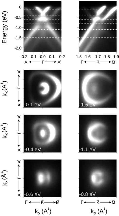
FIG. 2. Band dispersion recorded in the vicinity of the ¯Kpoint (top two panels) and angular distributions extracted at fixed energies close to the Dirac point. The six energies are shown as white dashed lines through the band dispersions in the top panels. The Fermi energy is located at 0 eV. An incident photon energy of 33 eV was used.
not correspond to that predicted for Bernal-stacked bilayer graphene [39,40].
B. DFT band structures
[image:4.608.50.295.69.513.2]The ARPES spectra presented in the previous section shows clearly the presence of twoπbands after Li deposition, which implies that Li has intercalated to the interface and decoupled the buffer layer from the substrate. This has previously been corroborated by both experimental core-level spectra and DFT calculations and verified in the current work (see Appendix). We will now address the relationship between the presence of Li between the two carbon layers and its effect on the dispersion by calculating the band structure of free-standing
FIG. 3. Calculated band structure of (a) AB-stacked clean bilayer graphene, (b) AA-stacked clean bilayer graphene (c) AB-stacked C8LiC8, (d) AA-stacked C8LiC8, (e) AB-stacked C6LiC6, and (f) AA-stacked C6LiC6. The high-symmetry labels are those of the graphene unit cell.
bilayer graphene with and without intercalated Li, and with different graphene stackings.
We first consider the case where Li does not intercalate between the two carbon layers. These two layers then remain Bernal stacked and the resulting band structure has a symmet-ric, parabolic band dispersion around the ¯K point, as shown in Fig.3(a). The band structure of clean AA-stacked bilayer graphene, shown in Fig.3(b), is comprised of two Dirac cones with linear dispersion, separated in energy by 0.5 eV.
FIG. 4. Band structure of free-standing C6LiC6as calculated with DFT (red solid lines) and using a tight-binding model (blue dashed lines), compared to the experimental ARPES spectra [cf. Fig.1(i)]. The calculated band structures have been shifted rigidly in energy to match the topπ∗band.
carbon sheets [42,43]. The resulting band structure is shown in Fig.3(d). It has the linear dispersion typical of AA-stacked bilayer graphene. The effect of the intercalated Li can be seen in the increased energy separation in the two Dirac cones, from 0.5 to 0.6 eV.
The highest concentration of Li found in GICs at ambient conditions is LiC6. The (√3×√3)R30◦ diffraction pattern observed after Li deposition at room temperature [13] would suggest that this Li concentration is also the most favourable in bilayer graphene. If we consider AB-stacked graphene with a C6LiC6 concentration, we find three π bands are visible, due to the asymmetric doping of the two graphene layers, as shown in Fig.3(e). Finally, we consider AA-stacked graphene at the same concentration. The energy dispersion, shown in Fig.3(f), is comprised of two Dirac cones shifted relative to one another by the interlayer coupling and with a gap opened in both at the ¯K point. We find that AA-stacked C6LiC6 is 36 meV/C lower in energy than the equivalent AB-stacked configuration. As a comparison, Bernal stacked clean bilayer graphene is 6 meV/C lower in energy than AA-stacked bilayer graphene.
Comparing the band structures presented in Fig.3with the experimental ARPES spectra in Fig.1(i), we find that good agreement is only achieved if we assume a C6LiC6 concen-tration of Li atoms between AA-stacked bilayer graphene. This is shown in Fig.4. The development of severe cracks and wrinkles after Li deposition [14] further supports this postulation. We suggest that this is due to the strain induced in the system when the top carbon layer attempts to shift to an AA stacking. These cracks do not appear when Li is deposited on the buffer layer only.
C. Tight-binding model
We will now discuss the unusual shape of the electronic band dispersion close to the Dirac point, and in particular the opening of gaps at the ¯Kpoint of the two Dirac cones, using a simple tight-binding model. The Li atoms, which intercalate in an ordered fashion, cause a periodic modification of the graphene electronic structure. The effect can be described
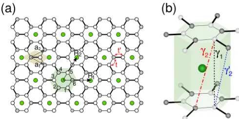
FIG. 5. Structure of C6LiC6. (a) Top view showing the graphene lattice vectorsa1and a2and the lattice vectors of C6LiC6, R1 and
R2. R1 and R2 are rotated by 30◦ with respect to a1 and a2 and are√3 longer. The two carbon sublattices are denoted with gray and white circles and Li atoms are shown as green circles. The two types of bonds associated with the Kekul´e textured graphene are shown as thin and thick solid lines. The two different intralayer hopping parameters between carbon atoms associated with these two bonds are denotedtandt. The six atoms belonging to the C6LiC6unit cell of one of the graphene layers are labeled 1–6, and are used to generate the Hamiltonian of the system. (b) Side view showing the interlayer coupling parameters,γ1 between carbon atoms directly on top of one another, andγ2 and γ2 describing the textured skew coupling terms.
by a periodic potential U(r)=U(r+l1R1+l2R2), where
R1 =n1a1+m1a2, R2=n2a1+m2a2, and a1 and a2 are the graphene lattice vectors [44].l,n, andmare integers. In our case,R1andR2describe the lattice vectors of C6LiC6as shown in Fig.5(a). Here, a1=(
√ 3 2 ,−
1
2)a0,a2=( √
3 2 ,
1 2)a0,
R1 =(
√
3,0)a0, andR2=( √
3 2 ,
3
2)a0, wherea0is the graphene lattice constant. A gap will open at the ¯K point when the periodic potential in reciprocal space,U(K), is not equal to zero. This condition will be satisfied when (n1−m1) mod 3= 0 and (n2−m2) mod 3=0. This rule is reminiscent of that describing the gap chirality in carbon nanotubes [45] and the effect has already been harnessed to open band gaps in monolayer and bilayer graphene through the periodic pattering of antidot lattices [46,47]. The triangular symmetry associated with a (√3×√3)R30◦Li adsorption pattern has already been shown to satisfy the conditions necessary to open a gap in monolayer graphene at the Dirac point [48,49].
We will now extend the model of Ref. [49] from Li decorated monolayer graphene to AA-stacked bilayer C6LiC6 graphene using a tight-binding model that takes the effect of the intercalated Li into account via a Kekul´e texturing of the nearest-neighbor hopping parameters. The 12×12 matrix that describes the Hamiltonian of such as system has the following form:
H =
HT HTB
HBT HB
,
[image:5.608.69.277.70.201.2]HT=HB, is given by ⎛ ⎜ ⎜ ⎜ ⎜ ⎜ ⎜ ⎜ ⎝
t 0 teik.τ1 0 t
t t 0 te−ik.τ2 0
0 t t 0 teik.τ3
te−ik.τ1 0 t t 0
0 teik.τ2 0 t t
t 0 te−ik.τ3 0 t
⎞ ⎟ ⎟ ⎟ ⎟ ⎟ ⎟ ⎟ ⎠ ,
where t and t are the textured nearest-neighbor carbon hoppings [see Fig. 5(a)], is the on-site energy and τ1,2=a0(
√ 3 2 ,∓
3
2) and τ3=a0(−
√
3,0). The interlayer coupling matrix,HTB=HBT, is given by
⎛ ⎜ ⎜ ⎜ ⎜ ⎜ ⎜ ⎜ ⎝
γ1 γ2 0 γ2e
ik.τ1 0 γ 2
γ2 γ1 γ2 0 γ2e−ik.τ2 0
0 γ2 γ1 γ2 0 γ2eik.τ3
γ2e−ik.τ1 0 γ
2 γ1 γ2 0
0 γ2eik.τ2 0 γ
2 γ1 γ2
γ2 0 γ2e−ik.τ3 0 γ
2 γ1
⎞ ⎟ ⎟ ⎟ ⎟ ⎟ ⎟ ⎟ ⎠ ,
whereγ1is the vertical interlayer coupling between two carbon atoms directly on top of one another andγ2 and γ2 are the textured skew hopping terms. These are sketched in Fig.5(b). The resulting band structure is shown by blue dashed lines in Fig.4. We find that, as a result of the intercalation symmetry, gaps open at the ¯K point of each Dirac cone. These two cones are then shifted in energy relative to one another with an energy equal to the magnitude of the vertical interlayer couping, |γ1| =0.34 eV. The in-plane hopping parameters,
t =2.79 eV andt=2.59 eV, agree with those found in in Ref. [49] to describe Li-adsorbed monolayer graphene. The values ofγ1= −0.34 eV andγ2=0.04 eV are characteristic of AA-stacked bilayer graphene and graphite [50].
In contrast to clean AA-stacked graphene or graphite, how-ever, the effect of the skew coupling terms,γ2andγ2, cannot be neglected. The effect of their textured nature on the band struc-ture can be seen in the breaking of the equivalence of the gaps at the ¯Kpoint of each Dirac cone. Ifγ2andγ2were equal, the gap opened in each cone would also be equal. Instead we have that one gap, Eg1, is 0.20 eV wide, while the other, Eg2, is 2.3 times larger, at 0.46 eV. This ratio is approximately equal to that betweenγ2andγ2, which are 0.10 and 0.04 eV, respectively.
To conclude, we have shown that Li intercalation serves to switch the stacking in a graphene bilayer from AB to AA. The highly-ordered Li layer generates a periodic perturbation of the graphene electronic structure such that a gap opens in each cone at the Dirac point. The increase in magnitude of the skew coupling terms is significant and its effects are visible in the experimental ARPES spectra.
IV. CONCLUSION
We have carried out detailed ARPES (angle-resolved photoelectron spectroscopy) studies of the band structure of monolayer graphene samples, before and after Li deposition at room temperature as well as after subsequent heating to 300◦C. Li intercalation is shown to have a large impact on the dispersion of the bands at energies close to the Dirac point, as well as donating charge to the graphene layers. Directly after
Li deposition we observe the appearance of a secondπband. Upon heating to 300◦C the electronic band structure changes significantly: theπbands become sharper and have a distinctly different dispersion to that of Bernal stacked bilayer graphene. To understand these observations, we performed density func-tional theory band structure calculations for Li intercalation in free-standing bilayer graphene for different stacking of the layers. Our combined experimental and theoretical results show that, after Li deposition and subsequent heating, Li both intercalates underneath the buffer layer—decoupling it from the substrate—and between the two carbon layers. In the process, it becomes energetically more favorable for the carbon layers to become AA-stacked rather than Bernal stacked. We show that theπ bands around the ¯K point closely resemble the calculated band structure of a C6LiC6 system, where the intercalated Li atoms introduce a periodic perturbation to the graphene electronic structure that opens gaps at the ¯Kpoint of the two Dirac cones.
ACKNOWLEDGMENTS
The authors wish to acknowledge the Swedish Research Council (VR) Grant Nos. 4252 and 621-2011-4426, the Swedish Foundation for Strategic Research (SSF) program SRL Grant No. 10-0026, the European Union Seventh Framework Programme under Grant Agreement No. 604391 Graphene Flagship and the Swedish Government Strategic Research Areas SeRC and in Materials Science on Functional Materials at Link¨oping University (Faculty Grant SFO-Mat-LiU No 2009 00971). R.A. acknowledges financial support from SRC VR Grant No. 621-2011-4249 and the Linnaeus Environment at Link¨oping on Nanoscale Functional Materials (LiLi-NFM) funded by VR. I.A.A. acknowledges the support from the Grant of Ministry of Education and Science of the Russian Federation (Grant No. 14.Y26.31.0005) and Tomsk State University Academic D. I. Mendeleev Fund Program (Project No. 8.1.18.2015). All calculations were performed using the supercomputer resources of the Swedish National Infrastructure for Computing (SNIC) at the National Supercomputing Center (NSC) and at the PDC Center for High Performance Computing (PDC-HPC).
APPENDIX A: LI-INTERCALATED GRAPHENE ON SIC(0001)
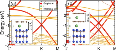
FIG. 6. Electronic band structure of (a) the Li intercalated zero layer graphene on SiC(0001) system and (b) Li intercalated monolayer graphene on SiC(0001). The Li concentration corresponds to LiC8 and LiC8LiC8, respectively. The insets show the relaxed structure of both configurations. The Fermi energy is located at 0 eV.
The band structure for the configuration that includes only zero layer graphene is shown in Fig.6(a). A singleπ band, associated with the now decoupled carbon layer, is visible. The Dirac point is located 0.93 eV below the Fermi energy due to the strong doping from the Li atom. Figure6(b)then shows the band structure of the configuration that includes a second carbon layer. Li atoms are now present both underneath the buffer layer and between the two carbon layers. As in the free-standing case, the AA-stacked configuration is energetically preferred. Two Dirac cones are now visible, separated in energy by 0.7 eV. This would suggest an interlayer coupling,γ1, of approximately 0.35 eV, similar to what we found for the free-standing intercalated bilayer. As a result of the doping due to these Li atoms, the Dirac points of the two cones are located 1.5 and 0.8 eV below the Fermi level, respectively.
APPENDIX B: REDUCTION IN DOPING AFTER HEATING Finally, we discuss the observation that the graphene doping level decreases significantly, from −1.4 to−0.6 eV, after heating to 300◦C [cf. Figs. 1(f) and 1(i)]. Core-level spectra shows that this dramatic reduction in doping occurs despite evidence that almost half of the Li atoms have not deintercalated or desorbed from the sample. The Li 1s core level spectrum shows that the component assigned to surface-adsorbed Li essentially disappears while the components assigned to intercalated Li remain, in agreement with earlier observations [13–15,24]. We therefore suggest that some Li atoms which were initially adsorbed on the surface, or between
FIG. 7. Side view of a 2×1 unit cell of SiC(0001) that includes two layers of graphene (16 C atoms in each) and three Li atoms. Isosurfaces of charge density difference show how charge is trans-ferred from a Li atom inserted (a) between the two carbon layers and (b) at the interface between SiC and the bottom carbon layer. A purple (orange) isosurface refers to a gain (loss) in charge density. The isosurface value is 0.0005 e/a.u.3.
the two graphene layers, intercalate to the interface between SiC and graphene after heating. In doing so, part of the charge which was previously transferred to the carbon atoms is now transferred to the SiC substrate, thus reducing the graphene doping level. If we consider a 2×1 SiC(0001) unit cell, that includes two graphene layers and three Li atoms, as sketched in Fig.7, we find that it is energetically more favourable, by 0.54 eV, for one of the Li atoms to move from between the two graphene layers to the interface between the substrate and the bottom graphene layer.
To visualize the charge transfer, we show in Fig.7(a)the charge density difference (CDD) that occurs when a Li atom is inserted between the top two carbon layers. The CDD is defined asρ =ρfinal−ρinital−ρLi, where ρfinal,ρinital, and
ρLiare the charge densities of the final system, the initial sys-tem that includes only two Li atoms, and an isolated Li atom, respectively. The charge is transferred equally between the two carbon layers. In contrast, Fig.7(b)shows how the charge is distributed from the Li atom when it is placed at the interface between SiC and the buffer layer. In this case, the majority of the charge is transferred to the substrate, with only a small amount transferred to the decoupled buffer layer. This process can explain the shifting of the Dirac cones towards the Fermi level after heating as observed in the ARPES spectra.
[1] C. Virojanadara, M. Syv¨ajarvi, R. Yakimova, L. I. Johansson, A. A. Zakharov, and T. Balasubramanian, Homogeneous large-area graphene layer growth on 6H-SiC(0001),Phys. Rev. B78,
245403(2008).
[2] Konstantin V. Emtsevet al., Towards wafer-size graphene layers by atmospheric pressure graphitization of silicon carbide,Nat. Mater.8,203(2009).
[3] E. Pallecchi, F. Lafont, V. Cavaliere, F. Schopfer, D. Mailly, W. Poirier, and A. Ouerghi, High electron mobility in epitaxial graphene on 4H-SiC(0001) via post-growth annealing under hydrogen,Sci. Rep.4,4558(2014).
[4] C. Riedl, C. Coletti, T. Iwasaki, A. A. Zakharov, and U. Starke, Quasi-Free-Standing Epitaxial Graphene on SiC Obtained by Hydrogen Intercalation,Phys. Rev. Lett.103,246804(2009). [5] Chariya Virojanadara, AA Zakharov, Rositsa Yakimova, and
Leif I Johansson, Buffer layer free large area bi-layer graphene on SiC(0001),Surf. Sci.604,L4(2010).
[image:7.608.50.295.70.179.2][7] Konstantin V. Emtsev, Alexei A. Zakharov, Camilla Coletti, Stiven Forti, and Ulrich Starke, Ambipolar doping in quasifree epitaxial graphene on SiC(0001) controlled by Ge intercalation,
Phys. Rev. B84,125423(2011).
[8] C. Xia, S. Watcharinyanon, A. A. Zakharov, R. Yakimova, L. Hultman, L. I. Johansson, and C. Virojanadara, Si intercala-tion/deintercalation of graphene on 6H-SiC(0001),Phys. Rev. B85,045418(2012).
[9] S. Oida, J. B. Hannon, and R. M. Tromp, Controlled synthesis and decoupling of monolayer graphene on SiC(0001),Appl. Phys. Lett.104,161605(2014).
[10] Nuala M. Caffrey, Rickard Armiento, Rositsa Yakimova, and Igor A. Abrikosov, Charge neutrality in epitaxial graphene on 6H-SiC(0001) via nitrogen intercalation,Phys. Rev. B92,
081409(2015).
[11] Andrew L. Walteret al., Highly p-doped epitaxial graphene obtained by fluorine intercalation,Appl. Phys. Lett.98,184102
(2011).
[12] Myriano H. Oliveira, Timo Schumann, Felix Fromm, Roland Koch, Markus Ostler, Manfred Ramsteiner, Thomas Seyller, Joao Marcelo J. Lopes, and Henning Riechert, Formation of high-quality quasi-free-standing bilayer graphene on SiC(0001) by oxygen intercalation upon annealing in air,Carbon52,83
(2013).
[13] Chariya Virojanadara, Somsakul Watcharinyanon, A. A. Zakharov, and Leif I. Johansson, Epitaxial graphene on 6H-SiC and Li intercalation,Phys. Rev. B82,205402(2010).
[14] Chariya Virojanadara, A. A. Zakharov, Somsakul Watcharinyanon, Rositsa Yakimova, and Leif I. Johansson, A low-energy electron microscopy and x-ray photo-emission electron microscopy study of Li intercalated into graphene on SiC(0001),New J. Phys.12,125015(2010).
[15] Somsakul Watcharinyanon, L. I. Johansson, A. A. Zakharov, and Chariya Virojanadara, Studies of Li intercalation of hydro-genated graphene on SiC(0001),Surf. Sci.606,401(2012). [16] Somsakul Watcharinyanon, Leif I. Johansson, Chao Xia, and
Chariya Virojanadara, Changes in structural and electronic properties of graphene grown on 6H-SiC(0001) induced by Na deposition,J. Appl. Phys.111,083711(2012).
[17] Andreas Sandin, Thushari Jayasekera, J. E. Rowe, Ki Wook Kim, M. Buongiorno Nardelli, and Daniel B. Dougherty, Mul-tiple coexisting intercalation structures of sodium in epitaxial graphene-SiC interfaces,Phys. Rev. B85,125410(2012). [18] Chao Xia, Somsakul Watcharinyanon, A. A. Zakharov, Leif
I. Johansson, Rositsa Yakimova, and Chariya Virojanadara, Detailed studies of Na intercalation on furnace-grown graphene on 6H-SiC(0001),Surf. Sci.613,88(2013).
[19] Aaron Bostwick, Florian Speck, Thomas Seyller, Karsten Horn, Marco Polini, Reza Asgari, Allan H. MacDonald, and Eli Rotenberg, Observation of plasmarons in quasi-freestanding doped graphene,Science328,999(2010).
[20] Andrew L. Walter, Aaron Bostwick, Ki-Joon Jeon, Florian Speck, Markus Ostler, Thomas Seyller, Luca Moreschini, Young Jun Chang, Marco Polini, Reza Asgari, Allan H. MacDonald, Karsten Horn, and Eli Rotenberg, Effective screening and the plasmaron bands in graphene,Phys. Rev. B 84, 085410
(2011).
[21] Somsakul Watcharinyanon, Chariya Virojanadara, and Leif I. Johansson, Rb and Cs deposition on epitaxial graphene grown on 6H-SiC(0001),Surf. Sci.605,1918(2011).
[22] Gianni Profeta, Matteo Calandra, and Francesco Mauri, Phonon-mediated superconductivity in graphene by lithium deposition,
Nat. Phys.8,131(2012).
[23] BM Ludbrook et al., Evidence for superconductivity in li-decorated monolayer graphene,Proc. Natl. Acad. Sci. USA112,
11795(2015).
[24] F. Bisti, G. Profeta, H. Vita, M. Donarelli, F. Perrozzi, P. M. Sheverdyaeva, P. Moras, K. Horn, and L. Ottaviano, Electronic and geometric structure of graphene/SiC(0001) decoupled by lithium intercalation,Phys. Rev. B91,245411(2015). [25] K. Sugawara, K. Kanetani, T. Sato, and T. Takahashi, Fabrication
of Li-intercalated bilayer graphene,AIP Adv.1,022103(2011). [26] Taisuke Ohta, Aaron Bostwick, J. L. McChesney, Thomas Seyller, Karsten Horn, and Eli Rotenberg, Interlayer interaction and electronic screening in multilayer graphene investigated with angle-resolved photoemission spectroscopy, Phys. Rev. Lett.98,206802(2007).
[27] A. H. Castro Neto, F. Guinea, N. M. R. Peres, K. S. Novoselov, and A. K. Geim, The electronic properties of graphene,Rev. Mod. Phys.81,109(2009).
[28] G. Kresse and J. Furthm¨uller, Efficient iterative schemes for
ab initiototal-energy calculations using a plane-wave basis set,
Phys. Rev. B54,11169(1996).
[29] G. Kresse and D. Joubert, From ultrasoft pseudopotentials to the projector augmented-wave method,Phys. Rev. B59,1758
(1999).
[30] P. E. Bl¨ochl, Projector augmented-wave method,Phys. Rev. B
50,17953(1994).
[31] J. P. Perdew, K. Burke, and M. Ernzerhof, Generalized Gradient Approximation Made Simple,Phys. Rev. Lett.77,3865(1996). [32] Hendrik J. Monkhorst and James D. Pack, Special points for
brillouin-zone integrations,Phys. Rev. B13,5188(1976). [33] Alexandre Tkatchenko and Matthias Scheffler, Accurate
Molec-ular Van Der Waals Interactions from Ground-State Electron Density and Free-Atom Reference Data,Phys. Rev. Lett.102,
073005(2009).
[34] Fredrik Owman and Per M˚artensson, The SiC(0001) 6√3× 6√3 reconstruction studied with STM and LEED, Surf. Sci.
369,126(1996).
[35] Wei Chen, Hai Xu, Lei Liu, Xingyu Gao, Dongchen Qi, Guowen Peng, Swee Ching Tan, Yuanping Feng, Kian Ping Loh, and Andrew Thye Shen Wee, Atomic structure of the 6H-SiC(0001) nanomesh,Surf. Sci.596,176(2005).
[36] M.-H. Tsai, C. S. Chang, John D. Dow, and I. S. T. Tsong, Electronic contributions to scanning-tunneling-microscopy im-ages of an annealedβ-sic(111) surface,Phys. Rev. B45,1327
(1992).
[37] J. Hass, R. Feng, T. Li, X. Li, Z. Zong, W. A. de Heer, P. N. First, E. H. Conrad, C. A. Jeffrey, and C. Berger, Highly ordered graphene for two dimensional electronics,Appl. Phys. Lett.89,
143106(2006).
[38] K. V. Emtsev, F. Speck, Th. Seyller, L. Ley, and J. D. Riley, Interaction, growth, and ordering of epitaxial graphene on SiC(0001) surfaces: A comparative photoelectron spectroscopy study,Phys. Rev. B77,155303(2008).
[39] M. Mucha-Kruczy´nski, O. Tsyplyatyev, A. Grishin, E. McCann, Vladimir I. Fal’ko, Aaron Bostwick, and Eli Rotenberg, Char-acterization of graphene through anisotropy of constant-energy maps in angle-resolved photoemission,Phys. Rev. B77,195403
[40] Choongyu Hwang, Cheol-Hwan Park, David A. Siegel, Alexei V. Fedorov, Steven G. Louie, and Alessandra Lanzara, Direct measurement of quantum phases in graphene via photoemission spectroscopy,Phys. Rev. B84,125422(2011).
[41] Isabella Gierz, J¨urgen Henk, Hartmut H¨ochst, Christian R. Ast, and Klaus Kern, Illuminating the dark corridor in graphene: Polarization dependence of angle-resolved photoe-mission spectroscopy on graphene,Phys. Rev. B83,121408
(2011).
[42] Yoji Imai and Akio Watanabe, Energetic evaluation of possible stacking structures of Li-intercalation in graphite using a first-principle pseudopotential calculation,J. Alloys Compd.439,
258(2007).
[43] JingJing Zhou, WeiWei Zhou, ChunMei Guan, JingQin Shen, ChuYing Ouyang, MinSheng Lei, SiQi Shi, and WeiHua Tang, First-principles study of lithium intercalated bilayer graphene,
Sci. China: Phys., Mech. Astron.55,1376(2012).
[44] Marc Dvorak, William Oswald, and Zhigang Wu, Bandgap opening by patterning graphene, Sci. Rep. 3, 2289
(2013).
[45] Stephanie Reich, Christian Thomsen, and Janina Maultzsch,
Carbon Nanotubes: Basic Concepts and Physical Properties
(Wiley-VCH Verlag GmbH, Weinheim, Germany, 2004).
[46] Ren´e Petersen, Thomas Garm Pedersen, and Antti-Pekka Jauho, Clar sextet analysis of triangular, rectangular, and honeycomb graphene antidot lattices,ACS Nano5,523(2010).
[47] Søren Schou Gregersen, Jesper Goor Pedersen, Stephen R. Power, and Antti-Pekka Jauho, Graphene on graphene antidot lattices: Electronic and transport properties,Phys. Rev. B91,
115424(2015).
[48] Z.-H. Pan, J. Camacho, M. H. Upton, A. V. Fedorov, C. A. Howard, M. Ellerby, and T. Valla, Electronic Structure of Superconducting KC8and Nonsuperconducting LiC6Graphite Intercalation Compounds: Evidence for a Graphene-Sheet-Driven Superconducting State,Phys. Rev. Lett. 106, 187002
(2011).
[49] M. Farjam and H. Rafii-Tabar, Energy gap opening in sub-monolayer lithium on graphene: Local density functional and tight-binding calculations,Phys. Rev. B79,045417(2009). [50] J.-C. Charlier, J.-P. Michenaud, and Xavier Gonze,
First-principles study of the electronic properties of simple hexagonal graphite,Phys. Rev. B46,4531(1992).