Adiabatic Split Level Charge Recovery Logic Circuit
Aruna Rani
EXTC Department
Dwarkadas J. Sanghvi College of Engineering Vile-Parle (West), Mumbai
Poonam Kadam
EXTC Department
Dwarkadas J. Sanghvi College of Engineering Vile-Parle (West), Mumbai
ABSTRACT
This paper describes the design and circuit simulation of split level charge recovery logic (SCRL). In conventional circuits the bits are thrown away for every transformation in the output level, And their associated energy becomes heat, which directly affects the cost of computation by increasing the system overhead required to get rid of the heat causing inconvenience of weight, short battery life etc. SCRL adiabatic logic promises to be an efficient technique to design low power digital VLSI circuit. The power efficiency of SCRL circuit is observed by comparing its performance with static CMOS inverter. A power efficient SCRL CLA is also designed and verified in this paper. Computer simulation using LTSPICE4 is carried out on SCRL circuit’s implemented using CMOS technology.
General Terms
Performance, Design, Verify.
Keywords
Low power, adiabatic Logic.
1.
INTRODUCTION
The vital trend of scaling in CMOS technology is the prime reason enabling today’s design capable of performing very high speed computations. As MOSFET inherently supports scaling, the complexity and number of devices on a given IC is no longer an issue [12]. With the growing use of portable devices proficient of performing computations comparable to desktop computers, it has become necessary to explore new design methodologies that would consume less power and provide high throughput. The concern of low power is becoming imperative even in non-portable applications where power is available. Interest in low energy computing is growing as the cost of power dissipation become preposterous [8,9].
Adiabatic computing is exact approach in this view point. Adiabatic circuits are those circuits which work on the principle of adiabatic charging and discharging [1]. The term adiabatic is derived from thermodynamics that describes a process in which there is no exchange of heat with the environment. Today’s novel adiabatic logic approach also offers a means to recycle the energy from output nodes instead of wasting this energy by discharging it to ground [4,5,6]. Conventional CMOS circuits achieve a logic ‘1’ or logic ‘0’ by charging the load capacitor to supply voltage Vdd and discharging it to ground respectively. As such every time a charge-discharge cycle occurs, an amount of energy equal to CV2dd is dissipated. Unlike the conventional CMOS circuits, in adiabatic circuits energy is recycled [8]. Instead of discharging the capacitor to ground, the charge is discharged to the power supply. SCRL is a fully adiabatic technique, which does not have non adiabatic loss. This paper focuses on
the concept and operation of SCRL. Also practical design considerations of implementing few basic gates are described. Some simulation results are also shown. Power comparison between CMOS logic circuit and SCRL circuit are performed.
2.
BASIC SCRL OPERATIONS
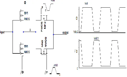
[image:1.595.321.564.323.470.2]The schematic of the SCRL inverter is illustrated in Fig 1. The SCRL inverter consists of a static CMOS inverter circuit with time varying supply followed by an additional transmission gate at the output [3].
Fig 1. SCRL Inverter and Power clocks Input
Fig 2. SCRL inverter output
[image:1.595.319.557.503.671.2]transmission gate at the output is gradually turned ON by swinging P and /P to Vdd and ground respectively. Then clock Φ and / Φ swing to Vdd to ground respectively. If the input to the gate is Vdd then the node marked x and the output will follow / Φ and ground and if the input was at ground the node x and output follow Φ and Vdd [3].
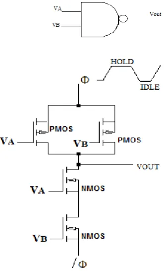
Fig 3 SCRL NAND gate
Fig 3 shows the symbol and schematic of a SCRL NAND gate. Although a static CMOS logic can be used for the same purpose, here power clocks is applied instead of Vdd and ground since the loading capacitance seen by clocks remain constant regardless of their input combinations, which is important for clock circuits.
3.
CARRY LOOK-AHEAD ADDER
In a digital system an adder is a fundamental component, so the design of the adder is selected to show the effectiveness of the adiabatic logic family. Adiabatic logic computes only one logic level per phase, so it’s difficult to put into operation a complex logic with a long chain of stages. Since a Ripple Carry Adder needs many phases to obtain a result, it’s not practical with the adiabatic method [2]. A 32-bit ripple carry adder would need at least 32- phases to carry out one addition. To overcome the drawback of an adiabatic circuit, CLA structure is adopted in the design of SCRL adder.CLA not only reduces logic depth, but also offers a pipelined structure if buffers are added in the circuit.
Carry Look Ahead Adders is used to avoid linear growth of the carry delay. In CLA the carries can be generated in parallel. The Carry of each bit is generated from propagate and generate signals (Pi, Gi) as well as the input carry (Co).
(1) (2) The carries from the four carry generator blocks are given by
(3) (4)
(5)
(6)
Fig 4 Block diagram of 4-bit Carry Look ahead Adder(CLA)
Fig 4 shows the block diagram of a 4 bit CLA adder. The carries C1 to C4 are generated in parallel from the four carry generator blocks (CG1-CG4) with the carry in signal C0 and propagate and generate signals serving as the inputs for the carry generator blocks[13]. The generate and propagate circuit is shown in Fig 5.
Fig 5 Generate and Propagate circuit
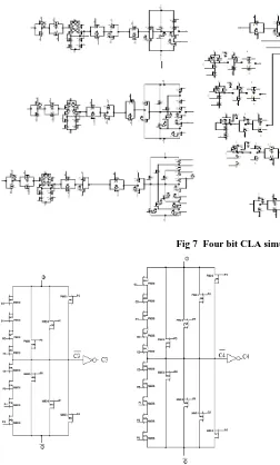
The Schematic 6 and 7 shows the static mirror circuit for four carry signals (C1 TO C4).
[image:2.595.58.224.143.419.2] [image:2.595.325.520.381.450.2] [image:2.595.320.536.516.713.2]Fig 7 Four bit CLA simulation in LTSPICE
Fig 8 SCRL C3 and C4 carry generator circuit
Fig. 7 is the complete schematic of a 4- bit carry look ahead adder circuit. The generate and propagate signals are generated in parallel and are fed to all carry generators with the input carry signals C0. The carry signals are generated simultaneously [11].
4.
ENERGY COMPARISION AND
RESULTS
Energy comparison is an interesting concern in adiabatic logic design. The energy loss of a conventional fully static CMOS including the discharge power-dissipation term is
and the above equation is the basis of the analysis of simulation results. Operating frequency term is excluded in this expression, so the energy loss equation represents energy loss per cycle. When the pull-up network is turned on, capacitor C charges up to through the ON resistance of the switch. The current through the resistance decreases exponentially over time [12]. The energy dissipation is equal to (1/2) .Where, is the voltage change at the node
out. Similarly (1/2) amount of energy is dissipated when pull-down network is ON. Thus overall energy dissipated by static CMOS circuit is . The transition at the output can be slowed down by using a time-varying voltage source instead of a static voltage supply. By spreading the transfer of charge to the capacitor over time, the current is greatly reduced [10]. If the current flow is maintained constant where T is total switching time, the total energy dissipation is reduced to (RC/T)
.SCRL saves the energy by returning
delivered energy back to the supply. The AC-power supply is needed to efficiently restore the charge, and thus it is required to design an efficient clock circuit which converts DC power to AC [7]. The SCRL inverter is already shown in Fig 1.and Fig 4.shows the basic static CMOS circuit. The energy CVDD 2
, which is consumed in the conventional CMOS circuits, is unavoidable since the charge is transferred from the supply and returned to the ground [10,12].
Fig.9 Static CMOS Inverter
[image:3.595.322.524.538.719.2]however, the supply voltage can be varied in a manner that would reduce the drain current, the energy will be significantly reduced. This can be achieved by using adiabatic circuits. Comparison of power dissipation between SCRL inverter and CMOS inverter is shown in the Table 1.
Table 1. Summary of Power dissipation of SCRL inverter Operating at 100MHZ
Technology
Power Dissipation (watts)
conventional CMOS inverter 1252uW
SCRL Inverter 290uW
power gain of SCRL over
conventional inverter 43%
conventional NAND gate 210uv
SCRL NAND gate 75uv
power gain of SCRL over
conventional NAND gate 28%
4.1 Simulations
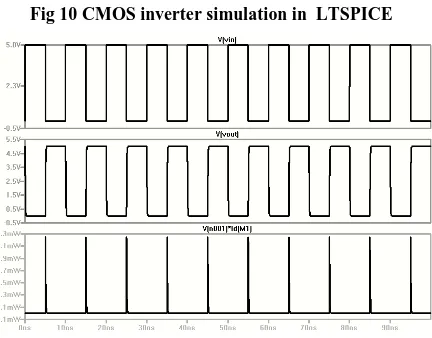
[image:4.595.317.549.71.420.2]The CMOS inverter is tested by LTSPICE simulation using a standard CMOS technology.
Fig 10 CMOS inverter simulation in LTSPICE
[image:4.595.57.285.157.327.2]Fig 11 CMOS inverter Simulation power, input and Output waveform in LTSPICE
Fig 12 SCRL inverter Simulation in LTSPICE
Fig 13 SCRL inverter Simulation output in LTSPICE
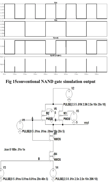
A SCRL NAND gate comprising of two NMOS transistors in pull down network connected in series and two PMOS transistors in pull network connected in parallel is simulated using a time varying supply and its power result is shown in the waveform.
[image:4.595.324.538.265.426.2] [image:4.595.336.533.530.707.2] [image:4.595.61.277.544.713.2]Fig 15conventional NAND gate simulation output
Fig 16 SCRL NAND gate Simulation
Fig 17 SCRL NAND gate Simulation output
This result shows that the SCRL reduces the energy consumption by about two (or four) times as compared to static CMOS logic in the 10MHz to 100 MHz range.
5.
CONCLUSION
This paper presents the Adiabatic SCRL logic. The performance of SCRL has less power dissipation as compared with that of static CMOS logic circuit. SCRL is a low energy adiabatic logic. Simulation indicates power saving over static CMOS circuits. Simulation of an inverter circuit, a two input NAND gate and 4 bit CLA circuit is studied. SCRL proves to
be a large power saving technique and shows the promising usage of SCRL in a low power system.
6.
REFERENCES
[1] A.G. Dickinson and J.S.Denker,”Adiabatic Dynamic Logic,” IEEE J.Solid-state Circuits,vol.30, pp.311-315,Mar,1995.
[2] Yong Moon, Deog-Kyoon Jeong,” An Efficient Charge Recovery Logic Circuit ,” IEEE J. Solid-State Circuits,vol,31.No 4, April, 1996.
[3] S. Younis and T.K. Knight, “Asymptotically Zero Energy Split- Level Charge Recovery Logic”. Proc. Workshop on low Power Design, pp.177-182, 1994. [4] S.Kim and M. C. Papaefthymiou, “Single-phase source
coupled adiabatic logic,” Proc. Int. Symp. Low-Power Electronics and Design, pp. 97-99, Aug. 1999
[5] W. C. Athas, L. J. Svensson, J. G. Koller, N. Tzartzains, and E. YC.Chou, Low-power digital systems based on adiabatic-switching principles,. IEEE Trans. Very Large Scale Intgr. (VLSI) Syst., vol. 2, no. 4, pp. 398.407, April 1994.
[6] J. S. Denker. A review of adiabatic computing. In Proceedings of the 1994 Symposium on Low Power Electronics/Digest of Technical Papers, pages 94–97, October 1994.
[7] J. S. Denker, S. C. Avery, A. G. Dickinson, A. Kramer, and T. R.Wik, Adiabatic computing with 2N-2N2D logic family,. in Proc. Int.Workshop Low Power Design, pp. 183.187, April 1994.
[8] K. T. Lau and F. Liu, .Improved adiabatic pseudo-domino logic,.Electron. Lett., vol. 33, no. 25, pp. 2113.2114, Dec. 1997.
[9] Y. Ye and K. Roy, .QSERL: Quasi-static energy recovery logic,. IEEE J. Solid-States Circuits, vol. 36, no. 2, pp. 239.248, Feb. 2001.
[10] K. Takahashi and M. Mizunuma, .Adiabatic dynamic CMOS logic circuit,. IEICE Trans. Electron. (Japanese Edition), vol. J81-CII, no. 10, pp. 810.817, Oct. 1998 (Electronics and Communications in Japan Part II (English Translation), vol. 83, no. 5 , pp. 50.58, April 2000).
[11] T. Gabara,“Pulsed Power Supply CMOS,” Technical Digest IEEE Symposium Low Power Electronics, San Diego, pp. 98- 99, October 1994.
[12] K. Kaishita, M. Hashizume, H. Yotsuyanagi, and T. Tamesada, .Low power dynamic CMOS logic circuits,. in Shikoku-Section Joint Convention Record of the Institute of Electrical and Related Engineers(Japanese Edition), p. 138, Oct. 2003.,