753
©IJRASET: All Rights are Reserved
Performance Evaluation of Ternary Content
Addressable Memory and 3T-2R TCAM
K. Vamsi Vardhanarao1, L. Srikanth2
1
Post Graduate Student, 2Asst Professor, Department of Electronics communication Engineering, GMRIT Engineering College, RAJAM, AP, India- 532127
Abstract: The content addressable memory (CAM) is implementing the functionality of the lookup table in a one clock cycle. It is utilizing dedicated circuitry. Ternary content-addressable memories (TCAM) is operating at low power dissipation and fast data recovery. The CMOS based TCAMs provides, fast data access by storing information in the SRAM cell, but it consumes high leakage power. The memristors are replaced with the SRAM cell, it gives the best solution for decreases leakage power. It takes less area compared to SRAM cell and also decreases the delay, stand by power of circuit and voltage swing at the matched line ML, by using a memristor device maximum power dissipation can be reduced along with area efficiency compared to Conventional TCAM. Here Comparison between NOR-type TCAM with memristor equivalent 3T-2R TCAM and PE TCAM is done in terms of power, area. The proposed design has 30% area efficiency and high-power consumptions compared to Conventional TCAM. Simulations are performed with the help of cadence software in 45nm technology.
Keywords: Ternary Content addressable memory (TCAM), 3T-2R TCAM, PE TCAM.
I. INTRODUCTION
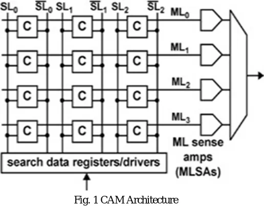
[image:1.612.183.441.441.645.2]Present days in human life one of the most important things is to access the internet with the high speed of data level. And the speed of internet services depends on the performance router. The router can be searching the IP address from the lookup table and packets promoting to the endpoint. The efficiency of the good network depends on the two factors one is a time delay and another one is packet transmission. Overcome these two factors, automatically increases the speed of the internet and the fast lookup table operation is searched and processed to the destination in less time. A software-based search is used. Content addressable memory (CAM) takes data as an input and gives the address as an output, with the help of the CAM user gets the location in which the data is stored. Searching speed of content addressable memory is higher than software-based search algorithms. CAMs are used in many routing applications and hardware such as network router, cache memories, etc… The architecture of cam is shown in fig.1
Fig. 1 CAM Architecture
Memristor is a semiconductor device. It has two terminals, in section II, III TCAMS has memristor components in the unit cell. Mainly they are used to store the data. So that here the memristor is replaced with SRAM and the resistance of the memristor is varied by the charge passes through the device. And memristor resistance depends on the amount charge flows through it.
754
©IJRASET: All Rights are Reserved
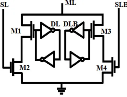
[image:2.612.202.408.236.394.2]stored. Here DL, DLB is high, then m1, m3 is off state. So that case, ml is always high due to irrespective of search lines. Because of don`t care (x) state, an extra state consumes high power, compared to the BCAM cell.
[image:2.612.131.484.423.568.2]Fig. 2 Basic TCAM cell
Table 1: Functionality of TCAM cell
STORED DL DLB SL SLB ML
0 0 1
0 1 HIGH
1 0 LOW
1 1 0
1 0 HIGH
0 1 LOW
X 1 1 X X HIGH
The 3T-2R TCAM cell has 3 transistors and 2 resistors and the functionality of the 3T-2R Based TCAM is shown in fig.3, a (PMOS) m1 is placed in between two memristors and gate terminal of the (NMOS) m2 & m3 transistors. And Von voltage is applied the m1. Pre is connected to the ground terminal, preb is connected to the gate terminal of m4 and the output of matched line is connected to the drain terminals of the m2 & m3. The tabular form of the 3T-2R TCAM is shown in table.2.
4) When the logic ‘0’ is stored in 3T-2R TCAM; [R1 = LOW R2 = HIGH]: If R1 = RL, R2 = RH then the stored value is ‘0’. And if SL = 0, SLB = 1 Then therefore searched data matches with the stored data matched line will be high And R1 = RL, R2 = RH and SL = 1, SLB = 0 Then stored data doesn’t match with searched data therefore ML discharges to ground.
5) When the logic ‘1’ is stored in 3T-2R TCAM; [R1 = HIGH R2 = LOW]: If R1 = RH, R2 = RL then the stored value is ‘1’. And if SL = 1, SLB = 0 Then therefore searched data matches with the stored data matched line will be high And R1 = RL, R2 = RH and SL = 0, SLB = 1 Then stored data doesn’t match with searched data therefore ML discharges to ground.
755
[image:3.612.244.398.80.207.2]©IJRASET: All Rights are Reserved
[image:3.612.133.480.240.406.2]Fig.3 3T-2R TCAM unit cell structure..
Table 2: Functionality of 3T-2R TCAM cell STORE
D
R1 R2 SL SLB ML
0 RL RH
0 1 HIGH
1 0 LOW
1 RH RL
1 0 HIGH
0 1 LOW
X RH RH X X HIGH
III. PRIORTY ENCODER TCAM
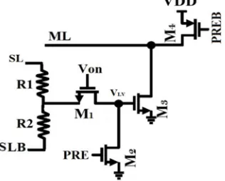
The operation of the PE TCAM design is similar to the 3T-2R TCAM. The NMOS transistor M1 is placed in between two memristors and gate terminal of the (NMOS) m2 & m3 transistors. Search data and stored data operations are the same as a 3T-2R TCAM cell. And this cell reduces the overhead of PE and it controls the three-phase of VLV. The comparison circuit memristors having different voltage levels according to the search outcome. Therefore using a sophisticated control method of the current flow through M3 (matched line current) IML based on 3T-2R TCAM to execute the priority encoding function during the search process. M4 is connected to the matched line (ML). The PE TCAM cell is connected to M4 that makeup one word. M4 is used to increase the ML voltage. M1 and M4 are the main components of the PE TCAM operation. These two transistors are used to control the priority encoding operation, The PE TCAM cell performs two phases of functions in a single operation. One is the evaluation phase and another one is the encoding phase. In the evaluation phase the search inputs SL/SLB is applied R1 and R2, The M1 is on at that time M4 is off state. M1 transfers the node point of the M2 and M3 to be different from one another according to the comparison result. Then matched line voltage preserves a precharge level Vss has no current path in between ML. And the second phase, during the encoding period M1 is off and M4 is on. In this case current flow through M4, ML voltage increases. Here Von changes from high level to low level, the current driving capability of ML is determined by VLV, which acts to block the charge accumulation of the matched line. The current flowing through the m2 reduces the matched line current. In this section, the process to explain the operation of the PE TCAM cell and shown in fig.4.
[image:3.612.249.407.590.717.2]756
©IJRASET: All Rights are Reserved
X R
H
R H
X X HIGH
IV. RESULT AND DISCUSSION
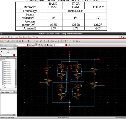
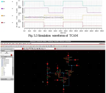
[image:4.612.145.467.82.257.2]The Ternary CAM, 3T-2R TCAM, and PE TCAM cells are implemented using cadence software 45nm technology. The Waveforms of TCAM, 3T-2R TCAM, and PE TCAM cell are shown in figures 5.3, 5.6 and 5.9 respectively. The waveforms we observed, the average power and the area values are shown in table.4.
Table 4: performance of TCAM, 3T-2R TCAM & PE TCAM
Parameter
BASIC TCAM
3T-2R
TCAM PE TCAM
Technology 45nm CMOS
Supply
voltage(V) 1V 1V 1V
Average
power(µw) 19.55 126.78 121.27
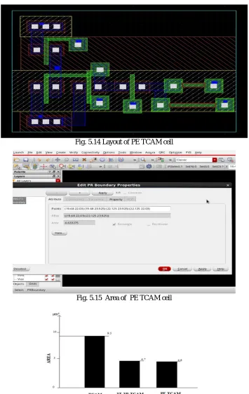
Area(µm²) 9.57 4.79 4.63
[image:4.612.98.527.312.718.2]757
©IJRASET: All Rights are Reserved
[image:5.612.129.497.75.268.2]Fig. 5.2 Test Bench of the circuit
By using cadence virtuoso software draw the schematic diagram and test bench of the tcam circuit. And shown in fig 5.1, fig 5.2.
Fig. 5.3 Simulation waveforms of TCAM
[image:5.612.129.497.384.709.2]758
[image:6.612.132.497.73.714.2]©IJRASET: All Rights are Reserved
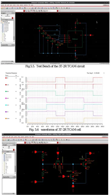
[image:6.612.135.492.77.292.2]Fig.5.5. Test Bench of the 3T-2R TCAM circuit
Fig. 5.6 waveforms of 3T-2R TCAM cell
759
©IJRASET: All Rights are Reserved
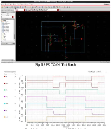
[image:7.612.135.491.75.486.2]Fig. 5.8 PE TCAM Test Bench
[image:7.612.127.501.505.719.2]Fig. 5.9 Simulation waveforms of PE TCAM cell
760
©IJRASET: All Rights are Reserved
Fig. 5.11 Area of TCAM cell
[image:8.612.146.485.67.727.2]Fig. 5.12 layout of 3T-2R TCAM cell
761
[image:9.612.136.491.71.633.2]©IJRASET: All Rights are Reserved
Fig. 5.14 Layout of PE TCAM cell
Fig. 5.15 Area of PE TCAM cell
Fig. 5.16 Area comparison in diffent cams
V. CONCLUSION
762
©IJRASET: All Rights are Reserved
AUTHORS PROFILE
K Vamsi Vardhanarao Received the B.Tech degree in (ECE) from JNTUK in 2016, Now he pursuing M.Tech Specialization in
(VLSI&ESD) (ECE Dept.) from GMRIT in JNTU Kakinada. His areas of interest are Low power electronics circuits and low power VLSI.
L. Srikanth, Assistant Professor in Department of ECE, GMR Institute of Technology, GMR Nagar, Rajam-532127, Srikakulam Dist.