Ni B Electroless Plating as Cap Layer for Ag Multi Level Metallization*
6
0
0
Full text
(2) 1616. M. Tsujimura, H. Inoue, H. Ezawa, M. Miyata and M. Ota Table 1 Contents of Ni–B EL chemicals. NiSO4 ·6H2 O. 0.1 mol/L. Malic acid. 0.1 mol/L. Glysine. 0.15 mol/L. DMAB. 0.1 mol/L. pH. 5 to 10 by ammonia 60◦ C–80◦ C. Temperature. Fig. 2 Test piece configuration.. 3.3 Polarization measurement Anode oxidization current and cathode reduction current are measured by the following conditions: (1) Anode oxidization current [Electrode] RE : Ag|AgCL|KCL(sat.). rials. Thus, DMAB (Dimethylamine borane) is adopted as a reducing agent, although sodium hypophosphite would generally be used otherwise. (3) Barrier effect: Since the semi-conductor device is exposed in several thermal processes, ensuring the barrier effect to avoid diffusion in the dielectric layer is required, i.e. thermal stability. (4) Controllability of deposition rate: Thinner cap layers are preferred, as long as the barrier effect can be maintained. The deposition rate must be decreased as compared to industrial plating processes.. CE : Pt wire WE : Ag plating 3 µm/Cu plate (Area 0.25 cm2 ) [Measured liquid] Malic acid : 0.1 mol/L Glycine : 0.15 mol/L DMAB : 0.1 mol/L pH : Adjusted by ammonia. 3. Experimental Method Test pieces are made as shown on 3.1, which have same configuration as an actual device. The cap material Ni–B is plated on these test pieces with the condition as shown on 3.2. Polarization features are measured to confirm plating basic performances as shown on 3.3. In order to confirm the barrier effect, test pieces are heated as shown on 3.4. In order to examine the mechanism of the barrier effect, element analysis is made as shown on 3.5. 3.1 Test piece configuration: See Fig. 2 (1) Ti (20 nm)/TiN (70 nm) is deposited as a barrier layer by sputtering. (2) Cu (200 nm) is deposited as an electrode layer by sputtering. (3) Ag metal is deposited by electrochemical plating under the following conditions Plating liquid: KAg(CN)2 0.03 mol/L; KCN 0.23 mol/L, pH: 11, Temp.: 298 K, pulse electric density: 10 mA/cm2 . (4) The dimensions of the test piece are 25 mm × 50 mm. 3.2 Plating conditions Electroless plating of Ni–B was used due to its selective performance with respect to metal. DMAB was selected as the reducing agent.2) Reports had indicated that Ni–B is crystalline if the B content is less than 10 at%, and amorphous if B content is not less than 10 at%.3) The chemical contents are listed in Table 1. In addition to main components listed in Table 1, several additives are included.. (2) Cathode reduction current [Electrode] RE : Ag|AgCL|KCL(sat.) CE : Pt wire WE : Ag plating 3 µm/Cu plate (Area 0.25 cm2 ) [Measured liquid] Malic acid : 0.1 mol/L Glycine : 0.15 mol/L NiSO4 ·6H2 O : 0.1 mol/L pH : Adjusted by ammonia and NaOH to 10. 3.4 Thermal treatment Test piece is tested under the condition of 400◦ C–1 h in 1.3 × 10⁻³ Pa Ar. 3.5 Element analysis B contents are measured by ICP (Auger Electron Spectroscopy). Barrier effect is measured by AES (Inductively Coupled Plasma). Crystallization is measured by XRD (XRay Diffraction). 4. Results and Discussion 4.1 Deposition rate Control of the deposition rate is a crucial factor affecting the cap layer. The thinner the deposits, the better, as long as.
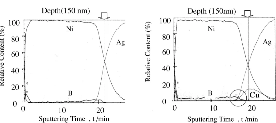
(3) 600. 1617. 16. 353 K. 14. 500. 12 400. 10. 300. 8 6. 200. 4 100. 2. 0. B Content (at ). Deposition Rate, DR /nm min-1. Ni–B Electroless Plating as Cap Layer for Ag Multi-Level Metallization. 0 4. 5. 6. 7. 8. 9. 10. 11. pH. 180. 5. Fig. 5 Anode polarization measurement.. pH10 4. 140 120. 3. 100 80. 2. 60 40. 1. 20 0 323. 328. 333. 338. 343. 348. 353. 0 358. Temperature, T/K Fig. 4 Deposition rate and B contents to temperature.. Cathode Current - Voltage (353K. Ammonia. 180. NaOH. 160 140. Electrode RE Ag AgCL KCL(sat.) CE Pt wire WE Ag plating 3 m/Cu plate Area 0.25cm2 Measured liquid Malic acid 0.1 mol/L Glycine 0.15 mol/L NiSO4 6H2O 0.1 mol/L pH Adjusted by ammonia and NaOH to 10. 120 100 80 60 40. the barrier effect is maintained. Thus, the targeted standard deposition rate is 100 to 200 nm/min, keeping the B content between 2 at% and 6 at%. Key parameters affecting the deposition rate are pH and temperature. First of all, the relationship between deposition rate and B content to pH is shown in Fig. 3. We were able to confirm that the deposition rate increased at pH levels up to 6, but decreased from pH 6 to 8. pH is controlled by ammonia. If pH 10 were adopted, the deposition rate would be around 200 nm/min and the B content less than 10 at%. Accordingly, a pH level of 10 was adopted. Next, the relationship of deposition rate and B content to temperature is shown in Fig. 4. It was confirmed that the deposition rate increases with temperature, while the B content was kept below 3% at a pH of 10. Based on these results, pH 10 and 353 K were adopted as standard conditions for electroless plating. 4.2 Polarization measurement In order to confirm the basic nature of electroless plating, anode and cathode polarization were measured. Anode polarization measurements are shown in Fig. 5, and cathode polarization measurements are shown in Fig. 6. As shown in Fig. 5, the oxidization current of DMAB to Ag could be obtained at a more non-noble side by adding ammonia to increase pH. The cathode current voltages in the case of ammonia and NaOH at 353 K are shown in Fig. 6. It was confirmed that reducing current to Ag of ammonia case is obtained at more non-noble side. Given these results, the plating conditions were set at. pH=10). 200. Current, A/ A m-2. 160. B Content (at ). Deposition Rate, DR /nm min-1. Fig. 3 Deposition rate and B contents to pH.. 20 0 -1.5. -1.3 -1.1 -0.9 -0.7 -0.5 -0.3 -0.1 Voltage(V) vs. Ag AgCL KCL(sat.) Fig. 6. Table 2. 0.1. Cathode polarization measurement.. Barrier effect of Ni–B by electroless plating.. B content. Ni–B thichkness. Barrier to Ag. Barrier to Cu. 3.2 at% 13.5 at%. 150 nm 300 nm. Effective Effective. Effective Not effective. pH 10 and 353 K. 4.3 Barrier performance Element analysis before and after thermal treatment was undertaken for the surfaces and below the surface by AES. It was confirmed in the case of Ni–B with 3.2 at% that Cu and Ag could not be detected on the surface after anneal from Fig. 7, and Cu diffused into the Ag metal layer as shown on Fig. 8, i.e. Ni–B with 3.2 at% has a barrier effect against Cu and Ag. It was also confirmed in the case of Ni–B with 13.5 at% that Cu was detected and Ag was not detected on the surface after anneal from Fig. 9, and that Cu diffused into the Ag metal layer as shown on Fig. 10, i.e. Ni–B with 13.5 at% does not have a barrier effect against Cu. The results are shown in Table 2..
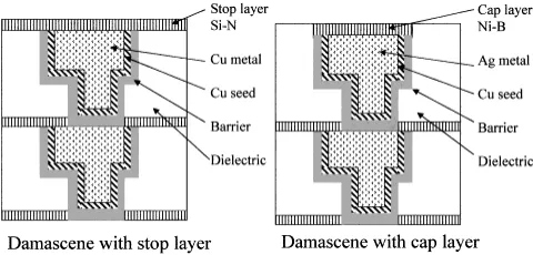
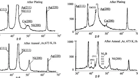
(4) 1618. M. Tsujimura, H. Inoue, H. Ezawa, M. Miyata and M. Ota. After Anneal ,Ar,673 K,1h. Intensity. Intensity. After Plating. (153) (64) (275). (185). Ni-B(3.2at%)150 nm. (153). Ag 500 nm. (64). Cu 200 nm (510). (510) (849). 500. Substrate. (849). (275). 1000. 500. 1000. Test piece construction. Kinetic energy (eV). Kinetic energy (eV). Fig. 7 Element analysis on surface by AES (Ni–B: 3.2 at%, 150 nm).. Fig. 8 Element analysis below surface by AES (Ni–B: 3.2 at%, 150 nm).. Table 3 Construction analysis of Ni–B by electroless plating. B content. Ni–B thichkness. Barrier to Ag. Barrier to Cu. 3.2 at% 13.5 at%. 150 nm 300 nm. Ni (crystalline) Amorphous. Ni (crystalline) Ni + Ni3 B. 4.4 Crystal structure An analysis of the crystal structure is shown in Fig. 11 (Ni–B: B 3.2 at%, 150 nm) and Fig. 12 (Ni–B: B 13.5 at%, 300 nm). Ni–B (Ni–B: B 3.2 at%, 150 nm) had a crystalline structure Ni(111) and Ni(200) before and after thermal treatment. However, Ni–B (Ni–B: B 13.5 at%, 300 nm) was confirmed to have an amorphous structure before treatment and a crystalline structure Ni(200) + Ni3 B afterwards. The results are shown in Table 3. 4.5 Barrier effect It was confirmed that the Ni–B layer with a reduced B content, such as 3.2 at%, exhibited a crystalline structure before. and after thermal treatment and that B was concentrated near the layer boundary between the Ag and Ni–B layers. It was assumed that the B concentrated near the layer boundary also existed in the grain boundary, and that this B interfered with the Cu diffusion in the grain boundary. On the contrary, in the case of Ni–B with a higher B content such as 13.5 at%, its structure changed from amorphous before thermal treatment to crystalline afterwards. It is assumed that Cu was diffused through the grain boundary created during this phase change. 4.6 Cap layer on damascene interconnects Damascene interconnects of Ag and cap layer of Ni–B were formed and are shown in Fig. 13. (Line and space is 1.0 µm × 1.0 µm, depth is 1.0 µm). The process flow is as follows: (1) trench etching by RIE (2) barrier sputtering of Ti 20 nm/TiN 70 nm (3) electrode sputtering of Cu 200 nm (4) CMP (5) electroless plating of Ni–B 100 nm.
(5) Ni–B Electroless Plating as Cap Layer for Ag Multi-Level Metallization. After Plating. 1619. After Anneal ,Ar,673 K,1h. (153) (64). Intensity. Intensity. Ni-B(13.5at. (510). (185) (153) (64). (849). (275). 500. Kinetic energy (eV). Ag 500 nm. (922) (510). (275). 1000. )300 nm. 500. (849). Cu detected. 1000. Cu 200 nm Substrate Test piece construction. Kinetic energy (eV). Fig. 9 Element analysis on surface by AES (Ni–B: 13.5 at%, 300 nm).. Fig. 10. Element analysis below surface by AES (Ni–B: 13.5 at%, 300 nm).. Fig. 11 XRD results (Ni–B: 3.2 at%, 150 nm).. Fig. 12 XRD results (Ni–B: 13.5 at%, 300 nm)..
(6) 1620. M. Tsujimura, H. Inoue, H. Ezawa, M. Miyata and M. Ota. Fig. 13 Damascene interconnects and cap layer.. It was confirmed that Ni–B was deposited selectively on Ag metal. 5. Conclusions (1) We confirmed that a Ni–B layer could be selectively deposited on Ag metal by the electroless plating method, using DMAB as the reducing agent. (2) A deposition rate of 150 nm/min and B content of 3.2 at% are obtained under conditions of pH 10 and temperature of 353 K. (3) It was confirmed that a Ni–B layer with 3.2 at%B content provides a barrier effect that prevents Ag and Cu diffusion through thermal processes. In this case, Ni–B remained crystalline before and after a thermal process.. (4) It was confirmed that a Ni–B layer with 13.5 at%B content does not provide a barrier effect that would prevent Cu diffusion through thermal processes. In this case, the structure of Ni–B changed from amorphous before to crystalline after the thermal process. (5) Damascene interconnects with Ag metal and Ni–B cap layer were formed as part of a trial effort. REFERENCES 1) S. Lopatin, Y. Shacham Diamand, V. Dubin, P. K. Vasudev, Y. Kim and T. Smy: Characterization of Electroless Cu, Co, Ni AND Their Alloys for ULSI Metallization Conference Proceedings ULSI XIII, (Materials Research Society, 1998) pp. 437–443. 2) I. Ohno: Electrical Chemical, 53 (1985) 196–201. 3) T. Hayashi: Electroless plating, (Nikkan Kogyo, 1994) pp. 41–42..
(7)
Figure


+3

Related documents
Few students have problems of managing moods (Mood Disorder). Very few students face problem of Attention Deficit Hyperactivity Disorder, Conduct Disorder
The case study aims to highlight the differences in the economic performance of the biorefinery supply chain when using exogenous biomass prices and forest industry production
1. Consider most appropriate form of disposal eg: charge, caution, advice file, no action etc. Ensure liaison is maintained with victim. Consider refusing/opposing bail
Er werden 2 vormen van behandelmotieven omtrent lijden genoemd namelijk lijden veroorzaakt door interne factoren (inadequate copingsvaardigheden en ruminatie/ piekeren) en
The axially magnetised permanent magnet found in the rotor of the hybrid stepping motor, is subject to demagnetising fields produced when current flows in the stator
Phase II trial of bevacizumab and erlotinib in patients with advanced hereditary leiomyomatosis and renal cell cancer (HLRCC) or sporadic papillary renal cell carcinoma. Motzer
To support this, the SV measured by the “reference” lidar has been compared against the SV measured by the “floating” lidar over the whole 38-day campaign (10-min data,
