Transmission Electron Microscopy Study on Microstructure
of Ag-Based Conductive Adhesives
Naoyuki Kawamoto
1;*, Yasukazu Murakami
2, Daisuke Shindo
2,
Yuichiro Hayasaka
3, Takeshi Kan
4and Katsuaki Suganuma
51World Premier International (WPI) Research Center for Materials Nanoarchitectonics (MANA),
National Institute for Materials Science, Tsukuba 305-0044, Japan
2Institute of Multidisciplinary Research for Advanced Materials, Tohoku University, Sendai 980-8577, Japan 3High-voltage Electron Microscope Laboratory, Tohoku University, Sendai 980-8577, Japan
4Electronics Materials Division, Fujikura Kasei Co., Ltd., Kuki 340-0203, Japan
5The Institute of Scientific and Industrial Research, Osaka University, Ibaraki 567-0047, Japan
We used advanced electron microscopy techniques to study the microstructure of Ag-based conductive adhesives, which are promising alternatives to Pb-free solders. Systematic microscopy observations revealed the development of connections between Ag agglomerates, when the weight density of Ag (Ag content) was increased up to 92 mass%. However, in a sample containing 94 mass% Ag, disconnection between well-defined Ag agglomerates and/or formation of voids between Ag-filler particles were observed. These results appeared to be consistent with the plot of resistivity versus Ag content: the resistivity decreased to a minimum value at 92 mass% Ag. We also demonstrated the formation of very small Ag particles in a thin-foil specimen subjected to electrical breakdown. This microscopic observation may be useful for understanding the process of electric breakdown in thin-foil specimens. [doi:10.2320/matertrans.MJ201022]
(Received April 28, 2010; Accepted June 1, 2010; Published July 14, 2010)
Keywords: transmission electron microscopy, conductivity measurement, discharge, electric breakdown, conductive adhesive, silver paste
1. Introduction
Development of new packaging materials such as Pb-free solders is of particular importance in materials science and engineering. As a result of the extensive research pursued in this regard in the last decade, Pb-free solders have been developed as alternatives to several types of conventional solders.1,2) However, the design of a Pb-free solder that is
resistant to high temperatures (up to 573 K) remains a challenge.3)Ag-based conductive adhesives, which consists
of an insulating epoxy resin and conductive Ag fillers, have attracted considerable attention because they are promising alternatives to Pb-free solders.4–7)The electric resistivity of a
cured Ag-based conductive adhesive (in commercial prod-ucts) is of the order of105cm, which is higher than that of metallic solders by two orders of magnitude. To increase the number of application of Ag-based conductive adhesives, the resistivity should be further reduced, at least to the order of 106cm. In this context, a microstructural analysis of the cured Ag-based conductive adhesive is important. Microstructural observations provide useful information that helps understand the mechanism of local conduction, which may be strongly affected by the form of agglomerations made of Ag fillers.
An unclear aspect related to the mechanism of conduction in Ag-based conductive adhesives is the relationship between the weight density of the Ag fillers and the resistivity. The resistivity decreases monotonically when the weight density of Ag (Ag content) is increased up to 92 mass%; however, with a further increase in the weight density, the resistivity starts to increase, as demonstrated in Fig. 1: refer to the section of experimental procedure for details of the resistivity measurement. The reason for this unexpected phenomenon is
not yet fully understood. Electron microscopy observations, which reveal the dispersion of Ag fillers in those specimens, may provide important information that helps in the analysis of these anomalous resistivity plots. Our electron microscopy study has been motivated by this unexpected behavior of Ag-based conductive adhesive.
In situelectron microscopy observations can be carried out on Ag-based conductive adhesives to identify the micro-structural changes that may be caused by the application of strong electric current. Some of the present authors have carried out simultaneous observations of the microstructure and the current-voltage (I-V) characteristics8) of thin-foil specimens of Ag-based conductive adhesive. They conducted an in situ experiment by using a special equipment called double-probe piezodriving holder,9,10) which is ideal for
Fig. 1 Relationship between resistivity and concentration of Ag fillers for Ag-based conductive adhesives containing 80 mass%, 88 mass%, 92 mass%, and 94 mass% flaky Ag fillers.
*Corresponding author, E-mail: [email protected]
Special Issue on Lead-Free and Advanced Interconnection Materials for Electronics
[image:1.595.327.521.372.547.2]carrying out conductivity measurements in a nanometer-scale area. On the basis of transmission electron microscopy (TEM) studies, they reported a close relationship between the morphological changes in the Ag fillers (probably caused by application of electric current) and the irreversible I-V characteristics of the specimen. We further expect that a microscopy observation offers a clue to understand the process of electric breakdown11–13) which is caused by an
excess voltage. For example, TEM observations may provide useful information about the conduction paths and/or the region of the specimen showing a significant temperature increase when excess current is applied to the specimen. This further motivated us to performin situTEM observations on Ag-based conductive adhesives.
This paper reports two types of microstructural investiga-tions on Ag-based conductive adhesives: (1) investigation of the relationship between the resistivity and changes in the internal structure (e.g., feature of dispersion of Ag fillers); (2) investigation of microstructural changes caused in the Ag fillers (in the form of thin films) when a high electric field of more106V/m is applied. The results of these observations can be used to obtain a thorough understanding of the mechanism of local conduction in Ag-based conductive adhesives.
2. Experimental Procedure
In this study, two types of Ag-based conductive adhesive specimens were employed: XA-5613 and XA-5617. The former (XA-5613), which comprised flaky Ag fillers, was used for a systematic study of the relationship between the
internal structure and the resistivity. XA-5613 specimens containing 80 mass%, 88 mass%, 92 mass%, and 94 mass% Ag fillers were prepared for SEM and TEM observations. XA-5617 specimens were used to carry out in situ TEM observations of the microstructural changes occurring upon the application of an applied voltage. The particle size and the resin composition of those specimens are summarized in Table 1. Note that the particle size is presented in terms of the median diameterd50%, which is graphically determined by the midpoint in the plot of the particle-size distribution. XA-5617 contained two types of Ag particles with different median diameter (particle type I: 6.7mm, and particle type II: 0.7mm), while the other specimens of XA-5613 had only one type of Ag particles (7.0mm). Both of these Ag-based conductive adhesives, XA-5613 and XA-5617, were pasted and cured on Cu substrate. The curing condition was at 423 K for 60 min.
The resistivity data shown in Fig. 1 were obtained by using the specimens (XA-5613) containing 80 mass%, 85 mass%, 86.5 mass%, 88 mass%, 92 mass%, and 94 mass% Ag fillers. The resistivity was determined by the four-terminal method in a constant electric current of 10 mA. The width and thickness of the specimens used in the resistivity measure-ments were 10 mm and 0.03 mm, respectively. The spacing between two probes to measure the potential drop (used in the four-terminal method) was 60 mm.
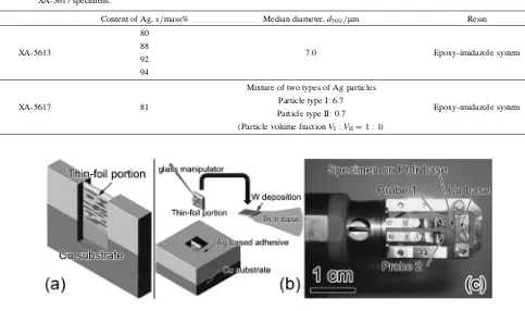
The specimens for TEM observations were made into thin foils by using a focused ion beam (FIB) apparatus (JEM-9310 FIB) (Fig. 2(a)). The thickness of the thin foils, which were used in conventional TEM observations, was approximately 100 nm. The method of preparation of another type of thin
XA-5617 specimens.
Content of Ag,x/mass% Median diameter,d50%/mm Resin
80
XA-5613 88 7.0 Epoxy-imidazole system
92 94
Mixture of two types of Ag particles
XA-5617 81 Particle type I: 6.7 Epoxy-imidazole system
Particle type II: 0.7
(Particle volume fractionVI:VII¼1 : 1)
[image:2.595.50.533.85.371.2]film for use in conduction measurements will be mentioned later in the text. Bright-field images of the thin foils were recorded by using a JEM-3000F transmission electron microscope. High-angle annular dark-field scanning TEM (HAADF-STEM) images were acquired by using an FEI Titan 80-300 transmission electron microscope. Chemical analysis of the specimens was performed by energy-dis-persive X-ray spectrometry (EDS) using the abovementioned FEI Titan 80-300 microscope. The acceleration voltage was 300 kV in all the TEM observations that were carried out in this study. The microstructures of the cured samples were observed by scanning electron microscopy (SEM) using a HITACHI-S4100 apparatus. The SEM images were obtained by using secondary electrons.
A different method of specimen preparation was adopted for the experiment in which voltage was applied to the thin foils. As shown schematically in Fig. 2(b), a thin foil (300 nm in thickness) was sliced off from the bulk sample of Ag-based conductive adhesive by using the FIB apparatus and a glass manipulator. The thin foil was put on a Pt-Ir probe tip. The
needle was fixed to a plate made of Cu (Cu base) in the double-probe piezodriving holder (Fig. 2(c)). The holder has two microprobes, both of which can be manipulated in three dimensions.9) A Keithley 2420 electric power supply was used in the experiment.
3. Results and Discussion
3.1 Correlation between microstructure and anomaly in resistivity plot
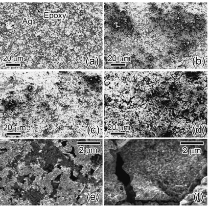
Figure 3 shows the SEM images of the specimens containing (a) 80 mass%, (b) 88 mass%, (c) 92 mass%, and (d) 94 mass% Ag.14)Bright portions in the images represent
Ag fillers. The dark portions represent the epoxy resin and/or the void produced during curing. In all the specimens, the Ag fillers are found to form agglomerates of the order of 1–10mm. The portion of the bright area appears to increase with an increase in the Ag content. More importantly, the observations indicate a close relationship between the dispersion of the agglomerates and the resistivity plot shown
[image:3.595.86.513.69.492.2]in Fig. 1. Although a large number of agglomerates are formed, as evident from Fig. 3(a), there exist non-metallic portions (shown in dark contrast) that separate the metallic agglomerates. As demonstrated in Figs. 3(b) and 3(c), connections are formed between the metallic portions (shown in bright contrast) when the weight density of Ag is increased. As shown in Fig. 3(c), there exists a wide area that includes a large number of Ag agglomerates. Interestingly, the resistivity is really minimized near the point of 92 mass%, as shown in Fig. 1. In contrast, a distinctive phenomenon is observed upon further addition of Ag fillers to this specimen. As shown in Fig. 3(d), the specimen with 94 mass% Ag includes well-defined, dense agglomerates whose sizes are of the order of 10mm. However, several of these agglomerates are likely to be separated by dark regions, which represent the voids and/or the naked epoxy resin. The difference in the microstructure can be discerned by another set of SEM images obtained in a higher magnification: refer to Fig. 3(e) and Fig. 3(f), which were collected from the specimens containing 92 mass% and 94 mass% Ag, respectively. As shown in Fig. 3(e), the connection of Ag agglomerates (bright portions) appears to be well developed in the specimen of 92 mass%. Although the size of Ag agglomer-ates is quite large in Fig. 3(f), they are surrounded by the well-defined insulator portions (dark portions). It is interest-ing to note that a slight change in the Ag content (92 mass% in Fig. 3(e) and 94% in Fig. 3(f)) results in the change as mentioned above in the microstructure. We anticipate that the disconnection of the agglomerates is a reason for the increase in resistivity observed in the heavily doped region (Ag content:>92mass%).
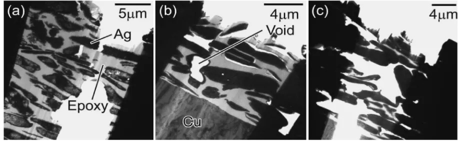
TEM observations as well provide useful information in understanding the microstructure of Ag-based conductive adhesives, although the images reveal only a limited area on the cured specimens. As shown in Fig. 4(a), which shows the image of the specimen containing 88 mass% Ag, the thin-foil region contains Ag fillers (the filler particles are stacked parallel to the surface of the Cu substrate) and the epoxy resin. Only a small number of intrinsic voids was observed in this specimen. Both the upper-right and lower-right portions were drop off the specimen when it was thin-foiled by using the FIB apparatus. The intrinsic voids, which must have been formed during the curing process, were more frequently observed in the specimens with a high density of Ag (for example, see the small void shown in the specimen with
92 mass% Ag (Fig. 4(b)). Voids occurred more frequently in the specimen containing 94 mass% Ag: the thin-foiled specimen showed a peculiar structure with many empty portions (Fig. 4(c)). The void formation makes the Ag filler particles detached from the epoxy resin which may mediate electric conduction when a very large voltage is supplied. Accordingly, the void formation appears to be another plausible mechanism explaining for the anomalous resistivity increase shown in Fig. 1 (>92mass%). Note that the interface between the Ag fillers in Fig. 4(a) is not as smooth as that between the fillers shown in Figs. 4(b) and 4(c). This was due to a chemical reaction (e.g., oxidization of the Ag fillers), which probably occurred as a result of prolonged exposure of the specimen shown in Fig. 4(a) to air at ambient temperature. No such reaction occurred in the other two specimens, as they were used for microscopy observations immediately after the FIB polishing.
In short, our electron microscopy observations have revealed two important features of the microstructures of Ag-based conductive adhesives. First, with an increase in the Ag content, connections may be developed between the Ag agglomerates, as demonstrated by the SEM images in Figs. 3(a)–(c). This trend is consistent with an idea of the percolation of individual metallic portions; the rate of percolation is expected to increase with the concentration of the Ag fillers. The second character is of the disconnection between well-defined Ag agglomerates and/or the formation of voids between Ag-filler particles, both of which suppress the electric conduction. Accordingly, the resistivity of Ag-based conductive adhesives should be affected by the crossover of these two competing features. It is reasonable to conclude that the anomalous increase in the resistivity when the weight density of Ag exceeds 92 mass% is attributed to the second feature.
3.2 Microstructural analysis of specimen subjected to electric breakdown
As mentioned in Introduction,in situelectron microscopy observation of electric conduction events in Ag-based conductive adhesives is also an interesting subject of research. The TEM observations in our recent study revealed the occurrence of morphological changes in the Ag fillers used in Ag-based conductive adhesives; such changes appear to influence the resistivity of these adhesives.8)In the present paper, we give a brief report of another application ofin situ
[image:4.595.67.525.73.214.2]observations performed using a double-probe piezodriving holder. The results in these observations have been obtained by using a thin-foil specimen. Nevertheless, the obtained results provide useful information for obtaining a thorough understanding of the behavior of Ag fillers under the influence of high current.
Figure 5(a) shows the experimental setup. A piece of the thin-foil specimen was pasted onto the tip of a Pt-Ir needle, which was grounded, by using a W deposition tool. This needle was placed in the double-probe piezodriving speci-men holder. An anode probe (made of a Pt-Ir needle) was brought in contact with a portion of the thin-foil specimen. Thus, an electric circuit such that shown in Fig. 5(a) was completed in the transmission electron microscope. Details of the experiments, such as the techniques used for surface cleaning of the probe tip, are provided in our recent paper.8)
Figure 5(b) shows the TEM image that was obtained before the application of voltage. The dark and gray portions represent the Ag fillers and the epoxy resin, respectively. Figure 5(c) shows the electron micrograph observed after supplying a voltage of 5 V, which resulted in electrical breakdown in the thin-foil specimen. After the electrical breakdown, several portions of the Ag agglomerates and the epoxy resin were probably destroyed. Furthermore, because of the breakdown, several agglomerates became spherical in shape, as indicated by the blue arrows. Small regions
in dark-gray contrast can be seen near the empty parts (destroyed by the electric breakdown), as indicated by the red arrow. It should be noted that the current density of incident electrons, which were used in the image acquisition, was only 1 A/m2. This is much smaller than the current density, 105A/m2, supplied to the specimen in the electric measurement as shown in Fig. 5. Furthermore, we could not observe an appreciable change in the microstructure with the exposure of the incident electrons only (without an applied voltage to the specimen). As far as these results are considered, the effect of incident electrons on the micro-structure can be negligible in this experiment, and the result in Fig. 5(c) can be attributed to the electric current/voltage supplied from the probe tip.
Figure 6(a) shows a HAADF-STEM image of a portion in the dark-gray contrast, such as the one indicated by the red arrow in Fig. 5(c). In general, the brightness of a HAADF-STEM image increases with the atomic number of con-stituents. This characteristic feature indicates that the bright dots in Fig. 6(a) represent Ag particles, which might have been dispersed in the epoxy layer (dark region) during the electrical breakdown. To confirm this prediction, EDS spectra were acquired from one of the bright dots (indicated by the red circle A) and a matrix portion (indicated by the red circle B); the results are shown in Figs. 6(b) and 6(c), respectively. The presence of Ag-L lines in the spectra
(a)
(b)
(c)
Fig. 5 (a) Schematic illustration of the electric circuit for supplying a local voltage to a thin-foil specimen. (b), (c) Bright-field images of thin-foil Ag-based conductive adhesive before and after electrical breakdown upon supplying a voltage, respectively.
[image:5.595.72.525.73.227.2] [image:5.595.67.523.278.427.2]line originated from the C atoms in the epoxy resin, and presumably from a small amount of contaminants in the specimen. The dispersion of these small Ag particles, whose diameter is of the order of a few nanometers, implies a significant temperature increase during the electrical break-down. Because of this temperature increase, the Ag fillers melt and/or evaporate within a short time. These observa-tions further indicate that such a significant temperature increase occurred in a small area near the electrode. In other words, we expect the distribution of the Ag particles (and/or related changes in the microstructure) to be indicative of the electric current path during electrical breakdown.
4. Summaries
We performed electron microscopy observations to ob-serve the microstructure of Ag-based conductive adhesives. The results obtained in the present study are summarized as follows.
(1) SEM observations reveal that with an increase in the weight density of Ag (up to 92 mass%) in the specimens, connections are formed between the Ag agglomerates. However, in the specimen containing 94 mass% Ag, several agglomerates appear to be disconnected by the epoxy resin and/or the voids that are probably formed during curing. TEM observations imply an increase in the number of voids within the cured Ag-based conductive adhesive when the weight density of Ag is increased.
(2) The aforementioned results indicate that the resistivity of Ag-based conductive adhesives is affected by the cross-over of the two tendencies, both of which are sensitive to the Ag content: (a) development of connections between the metallic agglomerates, and (b) disconnection between well-defined Ag agglomerates and/or the formation of voids between Ag-filler particles. It appears that the anomalous increase of resistivity, observed in the specimen containing 94 mass% Ag, can be attributed to the second tendency that is significant in the range of high Ag content.
(3) The observations carried out after applying a high voltage to a thin-foil specimen reveal the formed nanometer-sized Ag particles, which were dispersed in the epoxy layer.
breakdown in the thin-foil specimen. This implies that the changes in the microstructures of Ag-based conductive adhesives (e.g., dispersion of the Ag particles) can be used to identify possible conduction paths in the sample in the face of electrical breakdown.
Acknowledgements
This study was supported by the NEDO grant for the project ‘‘Development of Alternative to High-Temperature Lead Solders’’. This study was also supported by a Grant-in-Aid for JSPS Fellow (N. K.), Scientific Research (S), and Scientific Research (B) from the Japan Society for Promotion of Science.
REFERENCES
1) K. Suganuma: Curr. Opin. Solid State Mater. Sci.5(2001) 55–64. 2) I. E. Anderson: J. Mater. Sci.: Mater. Electron.18(2007) 55–76. 3) K. N. Tu, A. M. Gusak and M. Li: J. Appl. Phys.93(2003) 1335–1353. 4) D. Lu and C. P. Wong: IEEE Trans. Compon. Packag. Technol.23
(2000) 620–626.
5) D. Lu, Q. K. Tong and C. P. Wong: IEEE Trans. Electron. Packag. Manuf.22(1999) 223–227.
6) S. Ming, M. Loo and S. Dandia: Proc. Twenty-Sixth IEEE/CPMT Int. Electronics Manufacturing Technology Symp., (IEEE, Santa Clara, CA, 2000) pp. 279–287.
7) K. Suganuma: Kokomadekita Doudensei Secchakuzai Gijyutsu, (Kogyochosakai, Tokyo, 2004) [in Japanese].
8) N. Kawamoto, Y. Murakami and D. Shindo: J. Appl. Phys.107(2010) 044309.
9) Y. Murakami, N. Kawamoto, D. Shindo, I. Ishikawa, S. Deguchi, K. Yamazaki, M. Inoue, Y. Kondo and K. Suganuma: Appl. Phys. Lett.88
(2006) 223103.
10) N. Kawamoto, Y. Murakami, D. Shindo, K. S. Kim and K. Suganuma: J. Jpn. Inst. Metals70(2006) 384–388 [in Japanese].
11) J. V. Champion and S. J. Dodd: J. Phys. D: Appl. Phys.28(1995) 398– 407.
12) M. D. Noskov, A. S. Malinovski, M. Sack and A. J. Schwab: Tech. Phys.47(2002) 260–267.
13) F. Peruani, G. Solovey, I. M. Irurzun, E. E. Mola, A. Marzocca and J. L. Vicente: Phys. Rev. E67(2003) 066121.