Evolution in Metals. (Under the direction of Prof. Yuntian T. Zhu and Prof. Carl C. Koch).
Many material properties such as strength, ductility, thermal stability, irradiation resistance, etc. are determined by defects. When materials are subject to an extreme environment such as irradiation and high temperature, defects will further evolve and consequently result to very different configuration in microstructure. In this dissertation, the state-of-art works via direct transmission electron microscopy observation have been applied in order to provide deep understandings of defects and their evolution under such extreme environmental conditions. This work not only provides direct evidences for the defects formation and interaction, but also offers useful guidance to design materials with better properties.
As is known, it is the formation of nano-size Y-Ti-O enriched particles in microstructure that lead to high creep strength and enhanced irradiation damage tolerance for high temperature operations in ferritic oxide dispersion strengthened (ODS) alloys. Although Y/Ti based oxides have been extensively studied in the last decade, little is known whether there exist other type of oxides that have similar ultrafine sizes (<10nm) and dispersions in the matrix. In this dissertation work, new type of ZrO2 and HfO2 are observed in the Fe-14Cr
alloys with Zr and Hf additions, respectively via aberration-corrected scanning electron microscopy. The size and dispersion of these ZrO2 and HfO2 particles are comparable to
those of Y-Ti-O enriched oxides reported in irradiation-resistant ODS alloys, suggesting a potential application of the new alloy candidates for nuclear energy applications.
by Weizong Xu
A dissertation submitted to the Graduate Faculty of North Carolina State University
in partial fulfillment of the requirements for the degree of
Doctor of Philosophy
Materials Science and Engineering
Raleigh, North Carolina 2014
APPROVED BY:
_______________________________ ______________________________ Prof. Ronald O. Scattergood Prof. Suveen N. Mathaudhu
________________________________ ________________________________ Prof. Yuntian T. Zhu Prof. Carl C. Koch
DEDICATION
To my beloved wife, Yun.
BIOGRAPHY
ACKNOWLEDGMENTS
First I would like to express my deepest gratitude to my advisor Professor Yuntian Zhu and Professor Carl Koch for their steady guidance and patience in helping foster my development as a scientist during the past four years. Many thanks to Professor Suveen Mathaudhu for the immense knowledge he taught me, the insightful ideas and invaluable research experience he shared with me. I am also grateful to Professor Ronald Scattergood for his kindest supervision and the enlightening discussions we have made so many times throughout my graduate study. This thesis would not have been possible without your long-lasting encouragement, continuous funding, patience and guidance.
I am deeply indebted to Professor James LeBeau and Professor Thomas Rawdanowicz for their kind supervision and his great offer to sharpen my S/TEM skills while teaching their lab sessions of the course of Fundamentals of Transmission Electron Microscopy.
I would like to acknowledge the financial support from U.S. Army Research Office (W911NF-12-1-0009) and Department of Energy, Grant DE-NE0000538.
I would like to express my sincere appreciation for having the opportunity to cooperate with Dr. Yongfeng Zhang from Idaho National Laboratory, Dr. Paul Millett from University of Arkansas, and Dr. James Valdez from Los Alamos National Laboratory. I am especially grateful to Dr. Zhang for his selfless help and insightful suggestions in overcoming the difficulties during my research study.
I would like to thank Dr. Weiwei Jian for his very kind help during my graduate study. I wish to express my appreciation to Dr. Ming-Hung Tsai for his invaluable suggestions about doing research. I would like to express my sincere thanks to Dr. Guangming Cheng for his excellent advice, collaboration, and stimulating discussions. I am also grateful to Dr. Mostafa Saber for sharing his knowledge without reservation.
I wish to thank all the members of my research group who have made my life at North Carolina State University the most enjoyable journey: Haotian Deng, Lulu Li, Xiaolong Ma, Jordan Moering, Orm Piyawit, Xin Wang, Fan Wu, Hao Yuan, Yuchun Yuan, Liwen Zhang, Hao Zhou. I wish to thank all my dear friends inside and outside North Carolina State University for bringing me so many fond memories during my graduate life. A special thank you goes to Edna Deas and Mary Ann Lofgren for their enduring assistance whenever needed.
TABLE OF CONTENTS
LIST OF TABLES ... viii
LIST OF FIGURES ... ix
Chapter 1 Introduction ... 1
Chapter 2 Literature Review... 4
2.1 Radiation induced defects in crystals ... 5
2.1.1 Vacancy and self-interstitial ... 5
2.1.2 Dislocation and dislocation loops ... 18
2.1.3 Cavity and stacking fault tetrahedra (SFT) ... 28
2.2 Microstructure evolution and material damage under irradiation ... 33
2.2.1 Five stages of recovery ... 34
2.2.2 Radiation damage and void swelling ... 37
2.2.3 In-situ observation of defects interaction by TEM ... 43
2.3 Oxide dispersion strengthened (ODS) alloys and their nanostructured features ... 46
2.3.1 Synthesis of ODS alloys ... 47
2.3.2 Y-Ti-O enriched nano-size oxide... 49
2.3.3 Thermal and irradiation stability of ODS alloys ... 53
Chapter 3 Experimental Techniques... 59
3.1 Sample Preparation ... 59
3.1.1 Magnesium specimen... 59
3.1.2 Synthesis of Fe-14Cr alloys with Zr or Hf additions ... 59
3.2 Scanning/Transmission Electron Microscopy (S/TEM) ... 60
3.2.1 Sample preparation for S/TEM ... 60
3.2.2 In-situ TEM observation under electron Irradiation ... 63
3.2.2.1 Irradiation condition... 63
3.2.2.2 Effect of TEM foil thickness... 64
3.2.2.3 Stability of voids and c-components loops during the ―cool down‖ period ... 68
3.2.3 Thickness measurement using EELS ... 69
3.2.4 Aberration-corrected scanning transmission electron microscopy ... 70
3.2.5 Analysis of electron diffraction rings ... 71
3.3 Molecular Dynamic Simulation ... 72
3.3.1 Energy barrier calculation ... 72
3.3.2 Formation energy calculation ... 72
Chapter 4 In-situ Atomic-scale Observation of Irradiation-induced Void Formation ... 73
4.1 Introduction ... 73
4.2 Experimental Procedures... 75
4.2.1 TEM sample preparation and thickness measurement... 75
4.2.2 Electron irradiation conditions ... 76
4.2.3 Energy barrier calculation ... 76
4.2.4 Formation energy calculation ... 77
4.3.1 Void nucleation and early length growth ... 77
4.3.2 Void thickness growth. ... 80
4.3.3 Energy barriers for vacancy inter-facet diffusion ... 87
4.4 Discussion ... 89
4.5 Conclusion ... 92
Chapter 5 Dynamic Void Growth and Shrinkage in Mg under Electron Irradiation ... 94
5.1 Introduction ... 94
5.2 Experimental Procedures... 96
5.3 Results and Discussion ... 98
5.3.1 Statistics of Void Evolution ... 98
5.3.2 Void Coalescence ... 100
5.3.3 Interaction between self-interstitial atom (SIA) loop and void ... 103
5.4 Conclusion ... 108
Chapter 6 Nano ZrO2 Particles in Nanocrystalline Iron-Chromium-Zirconium Alloy ... 110
6.1 Introduction ... 110
6.2 Experimental Procedures... 113
6.3 Results ... 114
6.4 Discussion ... 120
6.5 Conclusion ... 124
Chapter 7 Microstructure and Nanocrystalline Stability of Iron-Chromium Alloys with Hafnium Addition ... 125
7.1 Introduction ... 125
7.2 Experimental Procedures... 129
7.3 Results ... 130
7.4 Discussion ... 143
7.4.1 Thermal stability mechanisms ... 143
7.4.2 The presence of oxygen and carbon ... 147
7.4.3 The precipitation of second-phases ... 148
7.5 Conclusion ... 150
Chapter 8 Conclusion ... 152
REFERENCES ... 157
APPENDIX ... 182
LIST OF TABLES
Chapter 2
Table 2.1 Threshold displacement energy of varies kinds of materials ... 9
Table 2.2 Formation and migration energy of vacancy in metals ... 12
Table 2.3 Formation energy of self-interstitials at different sites in hcp crystals ... 15
Table 2.4 Formation energy of self-interstitials in bcc metals with different configurations ... 16
Table 2.5 Migration energy of self-interstitials and the onset temperature of migration .. 18
Table 2.6 Summary of loop habit planes reported for hcp metals after neutron, ion and electron irradiation ... 26
Table 2.7 Summary of the microstructure observations in the annealed ODS powders. .. 50
Chapter 7
LIST OF FIGURES
Chapter 2
Figure 2.1 Schematic illustration of a Frankel pair formation when the material is
bombarded by a high energy electron. ... 6
Figure 2.2 Schematic illustration of a displacement cascade formation when materials are bombarded by an energetic neutron or ion. ... 7
Figure 2.3 Threshold displacement energy as a function of melting temperatures ... 10
Figure 2.4 The threshold displacement energy energies in Cu in different crystal orientations. (a) Calculated results from molecular dynamic simulation (b) experimental determination using electric resistivity ... 10
Figure 2.5 Octahedral sites and tetrahedral sites of interstitials in (a) fcc, (b) bcc, and (c) possible sites for interstitials in hcp crystal. ... 14
Figure 2.6 Dumbbell interstitials configurations in fcc along (a)<100> , (b)<110> (c) <111> direction, and in bcc along (d)<100> , (e)<110>, (f)<111> direction. . 15
Figure 2.7 Illustration of Crowdion configuration in fcc crystal along [110] direction ... 17
Figure 2.8 Atomic structures of (a) self-interstitial (b) vacancy type Frank loops formed in fcc crystal . ... 20
Figure 2.9 Atomic structures of perfect ½[110] (a) self-interstitial (b) vacancy loops in fcc crystal after unfault process ... 21
Figure 2.10 Experimental evidence of the unfault process of a self-interstitial dislocation loop in pure aluminum irradiated by 200 keV electrons. The yellow arrows indicated a loop before and after the transformation . ... 22
Figure 2.12 High resolution TEM image of a basal plane dislocation loops with Burgers vector b=⅙ 2 203
in Mg irradiated by 200 kV electrons. The stacking sequence is ABABABCBCB ... 25
Figure 2.13 Observation of voids in different materials (a) 316 stainless steel (b) Mo (c) Ni and (d) Zr ... 29
Figure 2.14 Formation of void lattice in Nb along (a) <100>, (b) <110> and (c) <111> zone axis ... 30
Figure 2.15 The specific energies of vacancy clusters in (a) Cu and (b) Fe ... 31
Figure 2.16 TEM of stacking fault tetrahedra (a) weak beam dark-field image in Cu
irradiated under 590 MeV protons irradiation, (b) high resolution TEM image in Ag ... 32
Figure 2.17 Formation of stacking fault tetrahedra (a) dissociation of Frank loops
b=⅓<111> (b) formation of the stir rod dislocations ⅙<110> (c) all six stair-rod dislocation are arranged . ... 33
Figure 2.18 Five stages of defect recovery for copper subject to electron irradiation at 4K 35
Figure 2.19 Comparison of dimensional size of aluminum rod before and after neutron irradiation (> 0.1MeV) with a total fluence of 1.5×10²¹ n/cm2. ... 39
Figure 2.20 Void swelling percentage as a function of dose in nickel, 316 stainless steel and Nimonic PE16 (Ni-Co based) super alloy, irradiated with carbon ions at 525ºC ... 40
Figure 2.21 Void swelling percentage as a function of temperature (T/Tm) in molybdenum and nickel. Solid dots show neutron irradiation (>0.1 MeV) with a fluence of 5×10²⁰ n/cm2 (Mo) and 2.3×10²⁰ n/cm2 (Ni). Open circlus show neutron irradiation (>0.1 MeV) with a fluence of 2.5×10¹⁹ n/cm2 (Mo) and 5×10¹⁹ n/cm2 (Ni) ... 40
Figure 2.23 Overview of JEOL ARM-1300S high-voltage transmission electron
microscope . ... 44
Figure 2.24 Overview of 200kV transmission electron microscope incorporated with heavy-ion accelerator installed in Sandia Natheavy-ional Lab ... 45
Figure 2.25 Overview of manufacturing process for ODS alloys . ... 48
Figure 2.26 Correlation between (a) Y/Ti ratio and Y-Ti-O enriched oxide particles, (b) particle size and oxide composition. ... 52
Chapter 3 Figure 3.1 Overview of SPEX 8000M Mixer/Mill ... 60
Figure 3.2 Overview of Struers TenuPol-2 twin-jet polishing machine ... 61
Figure 3.3 Overview of Allied MultiprepTM polishing machine ... 61
Figure 3.4 Overview of FEI Quanta 3D FEG dual-beam instrument ... 62
Figure 3.5 Illustration of FIB in-situ lift-out techniques. (a) Pt deposition, (b) Bulk milling, (c) U-shape cut, (d) Omniprobe lift-out, (e) thinning, and (f) final polishing. .. 63
Figure 3.6 Overview of JEOL JEM-2010F transmission electron microscope, equipped with Gatan electron energy loss spectroscopy (EELS) system. ... 65
Figure 3.7 Void morphology evolution in a thick irradiated region of 195 nm, for doses of (a) 2.5 dpa (b) 5.0 dpa (c) 7.5 dpa (d) 10.0 dpa. Voids are viewed along a [2110] direction. The scale bar is 20 nm. ... 66
Figure 3.9 HRTEM images of voids in a region (a) before and (b) after turn off the electron irradiation for 1 hour. ... 68
Figure 3.10 Electron energy-loss spectra (EELS) of an electron irradiated area. Thickness of this region is determined to be 70nm. ... 69
Figure 3.11 Overview of aberration-corrected FEI Titan G2 microscope. ... 71
Chapter 4
Figure 4.1 A series of HRTEM images of void length growth under electron irradiation. (a) A void (outlined by dashed lines) nucleated near the interstitial dislocation loop. (b)-(d), Stage 1 growth of the void, where it grew in length but not in thickness. The length growth direction is indicated by the yellow arrow. Detailed growth process is shown in Supplementary Movie 4.2. The specimen is irradiated over a dose range of 0.95-1.17 displacement-per-atom (dpa). The scale bar is 5 nm. ... 79
Figure 4.2 Void thickness growth in Stage 2 over a dose range of 2.27-2.36 dpa. (a) First vacancy layer nucleates on the top of the (0001) facet as indicated by an arrow. (b) The spreading of the vacancy layer on the (0001) facet, the size of the vacancy layer is designated by the dashed lines. (c) Vacancy layer extends over the whole (0001) facet surface. (d) Subsequent nucleation of a new vacancy layer (see Supplementary Movie 4.15 for more details). The scale bar is 5 nm.82
Figure 4.3 The formation of side facets of a void over a dose range of 3.37-3.41 dpa. (a) Facet plane indexes. (b) A vacancy layer nucleated on the (01 11) facet near its intersection with the (0001) facet. (c) The vacancy layer extended on the
(01 11) facet, which leads to (d) the growth of the (01 10) facet in the thickness direction. See Supplementary Movie 4.16 for more details. The scale bar is 2 nm. ... 83
Figure 4.4 Overview of the void shape and vacancy inter-facet diffusion paths. (a)
thick void (N=5). The image is projected along a [2 1 10] direction. Two possible different diffusion paths are considered due to the double lattice
structure in hcp . ... 84
Figure 4.5 HRTEM images of the void viewed along different orientations. (a) HRTEM images of voids when viewed along a [2110] direction with small thickness. The voids appear to have (0001) and (01 11) facets when their thicknesses are small. (b) when their thicknesses are larger, they have additional (0110)
facets. Voids are located between SIA loops (appear as line shape). (c) When viewed along a [0001] direction, voids appear hexagonal. (d) Void geometry when viewed along a [1100]
direction. The scale bars are 10 nm. ... 85
Figure 4.6 Specific formation energies of voids and basal plane vacancy dislocation loop versus the number of vacancies Nv. Green circles: Equilibrium void geometry (near equiaxed shape) as defined by the Wulff-construction adopting the {0001}, {01 10} and {01 11} surfaces. Red squares: Void of 5 atomic-layer thick (N = 5). Blue triangles: Void of 3 atomic-layer thick (N = 3). Yellow rhombs: Void of 1 atomic-layer thick (N = 1). Black rhombs: basal plane dislocation loop enclosing an extrinsic stacking fault. Among these vacancy clusters, the Wulff-shaped voids have the lowest specific vacancy formation energy Evf and is energetically most stable. For the plate-shaped voids, Evf decreases with increasing thickness N. For the basal plane vacancy loop, Evf is the higher than voids with thickness (N = 3 or larger) when the total number of vacancies Nv is small. When Nv is more than about 2500, the Evf of basal plane loop becomes smaller than that of a disk-shaped void with thickness N 5. ... 86
Figure 4.7 Void length and thickness variation with time under irradiation. Growth behaviors of two voids are compared. Both voids had a similar length growth rate in Stage 1, as well as thickness growth rate in Stage 2. In the later stage (over 1200 seconds), the length of void 2 shortened, which is similar to the trend found in zirconium[46, 71]. For void 1, however, the length of void 1 maintained nearly a constant value up to about 3000 seconds. ... 88
configuration. For example, the overall barrier for A B C path is determined as 0.20 eV (blue arrow), and the barrier for the reverse path
C B A is 0.41 eV (red arrow). Note that when a void is one atomic-layer thick (N=1), position G does not exist in the atomic configuration. ... 90
Figure 4.9 Energy barriers for vacancy diffusion between {0001} and {01 11} facets. (a) Energy barriers for forward diffusion along the path A B Cand its reverse diffusion (C B A) as a function of void thickness N. (b) Energy barriers for forward diffusion along the path D E F Gand its reverse diffusion (G F E D). ... 91
Chapter 5
Figure 5.1 Schematic illustration of the void morphology. (a) Overview of a void in three dimensions (3D). Voids are typically bounded by {0001}, {01 11} and {01 10} facets. (b) Projection of a void along a [2 1 10] direction. The void length, thickness and the dimension of {01 10} plane is marked as L, W and S,
respectively. ... 98
Figure 5.2 Statistics of void evolution behavior in the obvseved region with increasing irrdiation dosage. (a) Total void volume. (b) Average void length and thickness. ... 99
Figure 5.3 Evolution of (a) total number of voids and (b) number of newly nucleated voids within the irradiated region with increasing irratiation dosage. ... 100
Figure 5.4 The coalescence of two voids. (a) Ledges were formed when two voids met each other, as indicated by the green arrow. (b)-(f) Atoms on the ledges
gradually diffused out and filled the cavity in the dashed frame. The total length of the two voids decreased after coalescence (see Supplementary Movie 5.1). ... 101
Figure 5.6 Void shrink in length when it contacted with the edge of an extending self-interstitial atom (SIA) loop. (a) The loop is extending along (0001) basal plane towards the voids. The direction of loop extension is indicated by the blue arrow. (b) and (c) Voids shrank along length direction. (d) Voids vanish after the SIA loop extends over. (see Supplementary Movie 5.3) ... 104
Figure 5.7 The volume change of the void in Figure 5.5 (Supplementary Movie 5.3) as a function of the video recording time. This confirms that the void is undergoing volume shrinkage rather than a geometry change. ... 105
Figure 5.8 The void length grew as a SIA loop was passing through it. (a) and (b) Void shrank in size when it was located in front of an extending self-interstitial atom (SIA) loop edge. The extending direction of the SIA loop is indicated by the blue arrow. (c) and (d) The void began to grow in length when the SIA loop moved to its side (see Supplementary Movie 5.4). (e) Schematic illustration of a void located at the broad side of a SIA loop. Void tends to grow at this side. 107
Chapter 6
Figure 6.1 Microstructure of the Fe-14Cr-1.5Zr alloy after annealing for 1 hour at 900ºC. (a) Bright-field and (b) Dark-field image in TEM (c) Grain size histogram shows an average grain size of about 44 nm. ... 115
Figure 6.2 Formation of nanoparticles in the microstructure. (a) STEM high-angle annular dark-field (HAADF) image. Nanoparticles in dark contrast are uniformly distributed in the matrix. (b) Particle size histogram shows an average size of about 3.7 nm. (c) High-resolution TEM image of a grain boundary region. Some of these particles are located at a grain boundary, as indicated by the yellow arrows. ... 115
Figure 6.3 Energy dispersive X-ray spectroscopy (EDS) elemental mapping of an area near the grain boundary. (a) STEM high-angle annular dark-field (HAADF) image. Elemental mapping of (b) Fe-Kα, (c) Cr-Kα, (d) Zr-Kα and (e) O-Kα/Cr-L. Cr segregation is also found at some of the grain boundaries, as marked by the yellow arrows. ... 116
as illustrated by peaks covered by the light blue area. (b) Simulated electron diffraction pattern of ZrO2 in tetragonal and monoclinic crystal structure (red
lines) and bcc matrix (blue lines) as a function of the interplane spacing in reciprocal space (nm-1). The simulated pattern of tetragonal ZrO2 matches well
with the experiment data (light blue peaks). ... 118
Figure 6.5 High-resolution TEM (HRTEM) results of a ZrO2 particle. (a) HRTEM image
of the particle taken along a [010] zone axis. It appears bounded by several {002} and {011} surfaces. The orientation of the surfaces was marked on the top right side. The image also contained the phase contrast from the bcc ferritic matrix along a [120] direction. (b) Diffractogram showing the orientation relationship between the cluster (yellow color) and the matrix (blue color) as (002)ZrO2//(002)Matrix and [010]ZrO2//[120]Matrix. ... 120
Chapter 7
Figure 7.1 Microstructure of the Fe-14Cr-xHf alloy after annealing for 1 hour at 900ºC. TEM images for x equals to (a) 1 at.% Hf, (b) 2 at.%Hf, (c) 4 at.% Hf.
HAADF-STEM images for x equals to (d) 1 at.% Hf, (e) 2 at.%Hf, (f) 4 at.% Hf. ... 132
Figure 7.2 HAADF-STEM images of nano-size particles. (a) Some of particles are pinned at the grain boundaries (which are marked as yellow dash lines). The atomic resolution images of one particle located (b) at the grain boundary and (c) inside the ferritic grain are obtained. The distort region in (c) is drawn by a rectangular with yellow dash lines which includes a dislocation inside it. ... 133
Figure 7.3 Particle size histograms of the nano-size phase in the Fe-14Cr-xHf alloy where x equals to (a) 1 at.% Hf, (b) 2 at.% Hf, (c) 4 at.% Hf. The average particle sizes are 4.3 nm, 3.9 nm, 3.7 nm, respectively. ... 133
Figure 7.4 Chemical and crystal structure analysis of the nano-size particles. (a) Energy dispersive X-ray spectroscopy (EDS) mapping of the particle, which includes the HAADF-STEM image and the elemental mapping of the Hf, O, Fe, Cr species. (b) Selected area diffraction pattern of a region contains both the body centered cubic (bcc) ferritic matrix and nano-size particles in the Fe-14Cr-1Hf alloy. (c) Simulated electron diffraction patterns of HfO2 in orthorhombic,
Figure 7.5 Dark-field TEM images of the HfO2 particles in (a) 14Cr-1Hf alloy. (b)
Fe-14Cr-2Hf alloy. (c) Fe-14Cr-4Hf alloy (atom%). The dark-field TEM image is taken from the additional diffraction rings in figure 4b, suggesting that these diffraction rings belongs to the diffraction from these particles... 136
Figure 7.6 Selected area diffraction pattern of a typical sample region in (a) Fe-14Cr-2Hf alloy and (b) Fe-14Cr-4Hf alloy. ... 136
Figure 7.7 EDS elemental mapping of an area near the grain boundary in the Fe-14Cr-4Hf alloy. (a) HAADF-STEM image. Elemental mapping of (b) Hf-Lα, (c) Cr-Kα, (d) Fe-Kα and (e) O-Kα/Cr-L (f) C-Lα. As marked by the yellow arrows in (a), bright lines appear at grain boundaries in the HAADF-STEM image, which corresponds to Hf and Cr segregation in these areas. ... 138
Figure 7.8 EDS elemental mapping of a grain boundary area in the Fe-14Cr-4Hf alloy. (a) STEM HAADF image. Elemental mapping of (b) Hf-Lα, (c) Cr-Kα, (d) Fe-Kα, (e) O-Kα/Cr-L. (f) C-Kα ... 138
Figure 7.9 HAADF-STEM images of the Fe-14Cr-4Hf alloy. Hf and Cr grain boundary segregation has been shown as bright line features pointed out by the yellow arrows in (a) a typical region and (b) relatively rich region. ... 139
Figure 7.10 EDS elemental mapping of the Hafnium Carbides. (a) HAADF-STEM image, and elemental mapping of Hf-Lα, C-Kα, Fe-Kα, Cr-Kα and O-Kα/Cr-L. (b) HAADF-STEM images of a hafnium carbide and the corresponding cartoon of lattice projection view along [001], (b) [011] and (c) [112] direction. The Hf atoms is shown as blue dots, and C is shown as yellow dots. The STEM observation suggests a face-centered cubic structure of the phase which is consistent with the known hafnium carbide structure. ... 140
Figure 7.11 EDS elemental mapping and high resolution HAADF-STEM images of the M23C6 phase. (a) HAADF-STEM image and EDS elemental mapping (Cr-Kα,
C-Kα, Hf-Lα, Fe-Kα and O-Kα/Cr-L) of the M23C6 phase. The atomic ratio of
Cr to Fe within the carbide is determined to be 1:0.56 from the EDS data. The HAADF-STEM image, the simulated image (on the upper right corner of the HAADF-STEM image), and the cartoon of the lattice projection of the M23C6
Figure 7.12 EDS elemental mapping of a typical region of the Fe-14Cr-4Hf alloy (a) HAADF-STEM image and the elemental mapping of (b) Fe-Kα, (c) Hf-Lα, (d) Cr-Kα, (e) O-Kα/Cr-L (f) C-Kα and The Fe-Cr-Hf intermetallic particles are pointed out by yellow arrows. ... 142
Figure 7.13 Microstructure of the Fe-14Cr-1Hf alloy after annealing for 1 hour at 900ºC containing both μm size and ultrafine grains. (a) HAADF-STEM images (b) Bright-field TEM images of the same area. High density of nano-size HfO2
Chapter 1
Introduction
Nothing is perfect. This is absolutely right for materials. They inevitably contain a lot of defects in forms of vacancies, interstitials, dislocations, grain boundaries or cavities. Defects are important for materials since they determine many of material properties such as strength, ductility, thermal stability, conductivity, irradiation resistance, etc. The state-of-art works in materials science is to optimize the defect configuration or distribution in microstructure for better material performance. Experimentally, a number of processes have been employed to induce the defect evolution, such as thermal treatment, mechanical deformation, ion implantation or high energy particle irradiation. A deep understanding on how defects evolve during these processes not only helps clarify the correlation between material property and defect structure, but also provides useful guidance for designing better materials.
as energy dispersive spectroscopy (EDS) and electron energy loss spectroscopy (EELS), local chemical or bonding structure information that closely relates to defects becomes clearer.
One of the valuable features of TEM is its ability to carry out in-situ observation under electrons/ions irradiation or using special designed tensile/heating holders. It becomes increasingly interesting in performing in-situ TEM observation in recent years since it could simultaneously induce materials environment changes to observe the defects evolution. As is said: ―Seeing is believing‖, TEM provides a practicable way to reveal mechanisms that directly related to materials property changes and defects evolutions, which no other techniques can offer.
In this dissertation, in-situ observation of irradiation-induced void formation in magnesium is presented in Chapter 4. The observation of void nucleation and growth at the atomic scale resolution is presented for the first time. In Chapter 5, the dynamic motion of self-interstitial atom (SIA) dislocation loops and the corresponding void evolution are further investigated. These direct evidences provide fundamental understandings to help with the design and modeling of irradiation-resistant materials. The background knowledge of defects in crystals that are induced by high energy particles irradiation is reviewed in Chapter 2. The common experimental details used for the studies are given in Chapter 3.
Chapter 6 aims to provide an experimental discovery that new nano ZrO2 particles are
900ºC annealing. Very interestingly, the alloy shows similar particle dispersion in the microstructure to the oxide dispersion strengthening (ODS) alloys. The latter is known as a promising candidate for nuclear applications. The ODS alloys and the rationale of their irradiation damage resistance are also reviewed in Chapter 2.
In searching for other useful candidates to form nano-size dispersed oxides in microstructure, Fe-14Cr alloys with Hf addition are further investigated. In Chapter 7, similar Hf oxide dispersion in microstructure is studied with systematic variation with Hf addition. In addition, nanocrystalline stabilization mechanisms due to the HfO2 particle pinning and
Hf/Cr grain boundary segregation are directly revealed in this chapter.
Chapter 2
Literature Review
Many applications, such as nuclear plant, nuclear waste storage or outer space exploration requires materials to be reliable enough to withstand the extreme irradiation environment during their service lifetime [1-6]. The irradiation resistance becomes the critical issue in designing and selecting proper materials for nuclear applications. The studies on irradiation resistance have attracted more and more interests and studies in recent years.
When materials are bombarded by high energy particles such as neutrons, ions or electrons, atoms will be displaced from their equilibrium lattice sites and come to rest within the lattice as interstitial atoms. Consequently, point defects such as vacancies, self-interstitial atoms or their clusters will be introduced in materials microstructure at the first place. These defects will subsequently evolve into dislocations or cavities in a larger cluster size by diffusion, and will eventually result in materials property change or even materials dimensional variation, i.e. irradiation damage.
2.1Radiation induced defects in crystals
According to the geometrical dimensions, defects can be categorized into (1) 0D point defects: vacancies and self-interstitials, (2) 1D line defects: dislocation lines, (3) 2D planar defects: dislocation loops, (4) 3D volume defects: cavities, stacking fault tetrahedra (SFT). Among them, point defects are regarded to be the most basic ones since they can further evolve into other defects such as dislocation, cavities or SFTs depending on the irradiation temperatures and dose.
2.1.1 Vacancy and self-interstitial
Vacancies and self-interstitials are the primary products that generated from the collision events by the high energy particles. When an incoming energetic particle bombards the materials, it passes on certain recoil energy to the collided atom. If this recoil energy exceeds a critical value (called threshold displacement energy, Ud), this atom will be knocked
out of its lattice site, leaving a vacancy behind. Such displaced atom then comes to rest within the lattice and becomes a self-interstitial atom. After this event, a pair of a vacancy and a self-interstitial atom will be induced into the microstructure, called Frenkel pair as illustrated in Figure 2.1.
Figure 2.1 Schematic illustration of a Frankel pair formation when the material is bombarded by a high energy electron.
larger than the threshold displacement energy of the material. In this scenario, the displaced atom (called primary knock-on atom) will be energetically strong enough to further knock out other atoms in the lattice site during its movement. Again, the displaced secondary atoms may also gain enough kinetic energy to further displace other atoms in the lattice. As a result, a large number of vacancies and self-interstitials will be generated within one particle bombardment event, which is called displacement cascade[14, 15], as seen in Figure 2.2.
Figure 2.2 Schematic illustration of a displacement cascade formation when materials are bombarded by an energetic neutron or ion.
material is sensitive to defect concentrations in microstructure, defects of vacancies and self-interstitials that induced by the high energy electrons will thus increase the electrical resistivity of materials. By varying the incoming electron energy in the experiment, the threshold electron energy value Emin which does not cause resistivity increment can thus be
determined.
It is known that the threshold displacement energy Ud has correlation with Emin, which
can be expressed as [16]
2 min
min 2 2
min
2 2
( ) 2
d
mc E
U ME
M m c ME
(2.1)
where m and M are the mass of electron and recoiling atom respectively. Since m<<M, Ud
2
2 min
2
2 1 1
d E m U mc mc M
(2.2)
Crystal orientation could also affect the threshold displacement energy Ud. Bacon et al.
[18] calculated the Ud as a function of crystal orientations in Cu and Au as shown in Figure
2.4a. Similar trend was also seen in King et al. work from direct experimental measurement [19]. As seen in Figure 2.4b, the threshold displacement energy strongly varied with the orientations, i.e. being lowest along <110> and <100> direction, and becoming highest along <111> direction. Typically, the energy required to displace an atom will increase with the number of barrier atoms or their inter-atom distance, and decrease with distance of the closest approach to the barrier atoms[7]. The higher value of Ud near <111> direction
compared with that of <110> and <100> direction is most likely because this direction is perpendicular to the most close-packed {111} planes, and the distance of knocked out atoms to barrier atoms is the smallest. The orientation dependence of Ud is also seen in hcp metals.
Griffiths found that the <1120> orientation has the highest threshold displacement energy
(27.5 eV) in Zr, followed by <0001> (25.5 eV), <1010> (24.5 eV) and 112 3
orientation
(24.0 eV) [20].
Table 2.1 listed the experimental measurements of Ud and Emin for varies kinds of
materials [8, 16, 17]. Their melting points are also included for comparison. Figure 2.3 shows the plot of Ud as a function of the melting temperatures, in which Ud appears to be
suggests that material with large bond strength would be more likely to have better irradiation resistance.
Table 2.1 Threshold displacement energy of varies kinds of materials [8, 16, 17] Element Z Melting temperature
(K)
Emin
(kV) Ud
(eV)
Mg 12 923 100 10.0
Al 13 934 170 16.0
Si 14 1687 140 13.0
Ti 22 1941 320 19.0
V 23 2183 430 26.0
Cr 24 2180 28.0
Fe 26 1811 370 20.0
Co 27 1768 420 22.0
Ni 28 1728 440 24.0
Cu 29 1358 400 19.0
Zn 30 693 320 14.0
Ge 32 1211 370 15.0
Zr 40 2128 700 24.0
Nb 41 2750 800 33.5
Mo 42 2896 810 33.0
Pd 46 1828 890 34.0
Ag 47 1235 700 24.0
Cd 48 594 610 19.0
In 49 429.8 10.5
Sn 50 505 450 12.0
Nd 60 1289 9.3
Ta 73 3290 1230 33.0
W 74 3695 1300 35.0
Re 75 3458 44.0
Ir 77 2719 46.0
Pt 78 2041 1290 33.0 Au 79 1337 1300 33.0
Figure 2.3 Threshold displacement energy as a function of melting temperatures
Figure 2.4 The threshold displacement energy energies in Cu in different crystal orientations. (a) Calculated results from molecular dynamic simulation (b) experimental
Formation energy and migration energy are two parameters that determine the property of point defects. The formation energy of vacancy can be determined by measuring the vacancy concentration in the solids under thermal equilibrium, followed by the equation as below
f f f
v v v
G E TS
eq kT kT
V
C e e
(2.3)
where Gfv is the Gibbs energy of vacancy formation, Efv and Sfv is the enthalpy and entropy
of vacancy formation. k is Boltzmann constant, T is absolute temperature.
The thermal equilibrium vacancy concentration can be measured using varies kinds of methods such as capacity measurement, thermal expansion, quenching and annealing, positive electron annihilation experiment [21-23]. The summarization of the measured Efv is
given by Jung‘s and Wolfer‘s report [8, 16] as shown in Table 2.2. Regardless of different crystal structures, the value of Efv is proportional to the melting temperature of materials,
suggesting a close relationship between vacancy formation energy and bond strength.
The migration energy of vacancy can be obtained from diffusion coefficient measurement according to equation 2.4 as below
0 m v E kT v v
D D e (2.4)
Table 2.2 Formation and migration energy of vacancy in metals [8, 16] Crystals Z Melting temperature
(K)
Efv
(eV)
Emv
(eV)
Li 3 454 0.48 0.038
α-Be 4 1551 0.8 0.87
Na 11 371 0.34 0.03
Mg 12 923 0.8 0.5
Al 13 934 0.67 0.61
α-Ti 22 1941 1.27 0.6
V 23 2183 2.1 0.5
Cr 24 2180 2.1 0.95
Fe 26 1811 1.9 0.55
Ni 28 1728 1.79 1.04
Cu 29 1358 1.28 0.7
Zn 30 693 0.54 0.42
α-Zr 40 2128 1.79 0.84
Nb 41 2750 2.7 0.55
Mo 42 2896 3.1 1.35
Rh 45 2239 2.5 1.5
Pd 46 1828 1.85 1.03
Ag 47 1235 1.11 0.66
Ta 73 3290 3.1 0.7
W 74 3695 3.6 1.7
Re 75 3458 3.1 2.2
Pt 78 2041 1.35 1.43
Au 79 1337 0.93 0.71
Pb 82 601 0.58 0.43
0 m f v v E E kT atom V
D D e
(2.5)
(1) Located at the octahedral sites and tetrahedral sites of crystals. For fcc and bcc, their octahedral sites and tetrahedral sites are shown in Figure 2.5a and b, respectively. Note that in hcp crystals, because of their lower crystal symmetry, in addition to the octahedral sites and tetrahedral sites, other sites are also available for self-interstitial as seen in Figure 2.5c[26]. The corresponding formation energies of hcp metals at these sites are calculated by Bacon [26] in Table 2.3.
Table 2.3 Formation energy of self-interstitials at different sites in hcp crystals [26] Crystals Site Efi (eV)
Mg C 1.99
O 2.07 α-Ti C 3.68
BO 3.18, 3.85 BS/BC 3.01 α-Zr C 3.67, 4.59
O 4.59 BO 3.49, 4.59
Table 2.4 Formation energy of self-interstitials in bcc metals with different configurations[27]
Crystals <110> dumbbell
<111> dumbbell
<100>
dumbbell Crowdion Octahedral Tetrahedral V 4.23 4.72 4.98 4.7 4.84 4.82 Nb 4.54 4.88 4.85 4.95 4.91 4.95 Ta 6.97 7.32 8.16 7.31 8.08 7.75 Cr 4.14 3.58 3.99 3.58 4.04 4.09 Mo 7.08 7.28 7.23 7.24 7.61 7.58 W 9.71 9.02 9.88 8.99 10.06 10.05 Fe 3.93 3.98 4.75 3.99 4.77 4.43
Figure 2.7 Illustration of Crowdion configuration in fcc crystal along [110] direction
Although the formation energy of a self-interstitial can be lowered by forming the dumbbell or Crowdion configuration, its value is about 2-10 times larger than that of a vacancy. As a result, the self-interstitial concentration at the thermodynamic equilibrium (~10-15 m-3) is about 11 orders of magnitude smaller than that of vacancies (~10-4 m-3). Actually, sufficient amount of self-interstitial atoms could only be introduced into microstructures by severer plastic deformation or irradiation process.
self-interstitials could further diffuse to vacancy site causing recombination or further cluster together into other defects such as dislocation loops, known as Stage I recovery. The next section will introduce dislocations formed and their evolution behavior under the irradiation in detail.
Table 2.5 Migration energy of self-interstitials and the onset temperature of migration[8, 16]
Crystals Onset temperature
for migration (K) E
m i (eV)
Fe 23-144 0.25-0.32
Mo 33-39 0.083
W 11-38 0.054, 0.085
Ag 15 0.085, 0.088
Al 37 0.112, 0.115
Cu 38 0.117
Ni 56 0.14, 0.15
Pb 4 0.01
Pt 22 0.06-0.07
α-Co 45-50 0.1-0.15
Mg 13 0.029
Re 90 0.16
Zn 13 0.015
α-Zr 102 0.26, 0.30
2.1.2 Dislocation and dislocation loops
Frank-Read or double cross slip mechanisms. Since the basic features and properties of dislocations are reviewed in many literatures [7, 28, 29], the following section will be specifically focused on the mechanism of how dislocations are introduced by irradiation and their subsequent growth behaviors.
At the beginning stage of irradiation, dislocations are usually presented in the form of dislocation loops with diameters ranging from few nanometers to 100 nm due to the aggregation of point defects. These dislocation loops usually contain stacking fault when they are nucleated.
Figure 2.8 Atomic structures of (a) self-interstitial (b) vacancy type Frank loops formed in fcc crystal[29].
From Fisher and Alfred[30], the energy per unit length of a dislocation faulted loop is given by 2 0 ln 4 Kb R E r
(2.6)
where b is the loop Burgers vector, R is the outer limit of the dislocation strain field, r0 is
the cut-off core radium, K is the anisotropy factor that is related to the Poisson ratio and the elastic moduli.
For simplicity, considering a circular faulted loop in a diameter of d with stacking fault energy γ, the energy of this loop per unit length will be
2
0
ln
4 4
Kb R d
E
r
(2.7)
mechanism of this transformation was revealed from MD simulation via the nucleation and extension of certain partial dislocation loop on its fault plane[31]. As a vacancy loop for example, it is known that the stacking sequence across the loop is ABCACABC. If a slip of partial dislocation changes the stacking sequence to be CB, BA, and AC, it will change the stacking sequence of the vacancy fault loop (ABCACABC) to be ABCABCAB and restore the lattice to normal fcc sequence, which means the loop is unfaulted. The corresponding dislocation reaction can be seen in equation 2.8.
1 1 1
[111] [121] [101]
3 6 2
(2.8)
Figure 2.9 Atomic structures of perfect ½[110] (a) self-interstitial (b) vacancy loops in fcc crystal after unfault process[29].
experimental observation of pure aluminum specimen under the 200kV irradiation as shown in Figure 2.10.
1 1 1 1
[111] [112] [121] [011]
3 6 6 2
(2.9)
Figure 2.10 Experimental evidence of the unfault process of a self-interstitial dislocation loop in pure aluminum irradiated by 200 keV electrons. The yellow arrows indicated a
loop before and after the transformation.
more favorable than that in fcc metal. Followed by the two mechanisms expressed in the dislocation reactions as follows, two kinds of perfect dislocation b=½<111> and b=<100> can form. The formation of dislocation loop with b=<100> are important to Ferritic steel. As showed by Little et al[32], the existence of high density <100> loops in steel intrinsically define the enhanced void swelling resistance of steels. It should be noted that the <100> loops may also directly form from the self-interstitials accumulation from <100> dumbbells, despite their high formation energy.
1 1 1
[110] [001] [111]
2 2 2 (2.10)
1 1
[110] [110] [100]
2 2
(2.11)
In hcp metals, dislocation loops can be seen on prism {10 10}, basal {0001}, or pyramidal{10 10}planes. In general, loops on these planes has Burgers vector b= ⅓1120,
⅙ 2203 (or ½[0001] ) and ⅓ 1123 , respectively. A schematic illustration of corresponding habit plane and Burgers vector can be seen in Figure 2.11.
On prism plane, a fault loop with Burgers vector b= ⅓10 10 could nucleate and grow at very beginning, then followed by the transformation process to become a full dislocation loop via the following dislocation reaction.
1 1 1
[1010] [1210] [112 0]
2 6 3
Figure 2.11 Schematic illustration of habit plane and lattice vector direction in hcp crystal
For prismatic plane loops, since they are perfect dislocations, no further unfault process is needed.
For basal plane loops, interestingly, no mechanism can be applied to unfault the dislocation loops with Burgers vector b=½<0001> by transferring them to a full dislocation. In a different way, the basal plane ½<0001> loop could lower the loop energy by changing its stacking fault type to a lower energy configuration (I1 stacking fault). This process can be realized followed a dislocation reaction shown in equation 2.13. The dislocation loop with such low energy configuration is shown in Figure 2.12.
1 1 1
[1100] [0001] [2 203]
3 2 6
Figure 2.12 High resolution TEM image of a basal plane dislocation loops with Burgers vector b=⅙2203 in Mg irradiated by 200 kV electrons. The stacking sequence is
ABABABCBCB.
Besides that, the loop can further reduce its formation energy by forming a second loop on its fault plane so that the stacking fault can be removed. Such double-layer loops are experimentally observed in Zn, Mg and other hcp metals[33, 34]. In a similar way, triple-layer or fourth-triple-layer can also be seen in Mg subject to the quench and annealing process [34, 35].
different hcp metals and their possible habit plane for loop formation are summarized in Table 2.6[38].
Table 2.6 Summary of loop habit planes reported for hcp metals after neutron, ion and electron irradiation[38]
Crystals c/a 300K Melting
temperature (K) Primary loop habit plane
Homologous temperature
α-Be 1.568 1557 prism 0.24
basal 0.43
α-Hf 1.581 2493 prism 0.28-0.32
Ru 1.582 2773 basal, prism 0.24-0.40 α-Ti 1.587 1941 prism, pyramidal 0.37
prism (basal) 0.3-0.4
prism 0.3-0.4
Gd 1.59 1623 basal 0.17-0.41
α-Zr 1.593 2133 prism 0.14-0.34
prism (basal) 0.32 prism, pyramidal 0.17-0.36 prism, pyramidal and basal 0.32-0.34
Re 1.615 3423 prism 0.4
α-Co 1.623 1765 prism 0.17
basal 0.01
Mg 1.623 923 prism 0.11-0.33
basal 0.33
prism, basal 0.33-0.54
Zn 1.856 692 basal 0.21-0.43
Cd 1.886 594 basal 0.24-0.51
(with Fe, Mn, Cu, Zn impurities <1ppm), it is found that the prism loops are the dominant loops in microstructure under irradiation, in which both vacancy and interstitial type of prism loops can be observed[38]. Nevertheless, irradiation of less pure specimen (100 ppm) results in both basal and prism loops formation in microstructure[39]. Another difference between impure and pure Mg is that the loop density was typically an order of magnitude larger than that of very pure sample with similar irradiation condition, while their loop size became smaller[38, 40]. In Mg with commercial purity (500ppm), Khan reported that basal plane interstitial loops were the dominated loops after the electron irradiation, although small density of vacancy type prism loops were observed in microstructure[41, 42]. Other factors such as stacking fault energy, temperature, anisotropic diffusion, dislocation bias, lattice strain will also affect the loop habit plane, which is reviewed by Griffiths in [37, 38].
behavior in Mg is closely related to the dynamic motion of c-component dislocation loops from the in-situ observation.
2.1.3 Cavity and stacking fault tetrahedra (SFT)
Cavity is one of the most important defects in irradiated materials. Cavities have been reported to form in almost all crystalline materials under irradiation[38, 57, 59-66]. The first observation of cavity formation can be traced back in 1967 when Cawthorne and Fulton reported small voids of ~21 nm in size in 316 stainless steel under the neutron irradiation[59]. From then on, increasing attentions have been given on cavity formation, since it will lead to the volumetric swelling problem of the material. Typically, cavities are divided into two categories in terms of the geometry, i.e. voids and bubbles.
usually called void lattice. Void lattice has been frequently observed in bcc materials, but similar aligned void structure could also be seen in fcc or with less perfect void alignment in hcp metals[76]. Many theories and models were proposed for void lattice formation on the basis of non-linear diffusion of defects and their interactions between voids[76-79]. One dimensional migration of interstitials and their clusters is now generally accepted to be responsible for void lattice formation[80].
Figure 2.14 Formation of void lattice in Nb along (a) <100>, (b) <110> and (c) <111> zone axis[75].
Figure 2.15 The specific energies of vacancy clusters in (a) Cu and (b) Fe[81].
Formation of cavities required a temperature range from 0.3-0.6 Tm (Tm is the material
melting point) and relative high dose. The density of cavity typically increases with dosage increment, and approaches to a platform for above 1-50 dpa. But their total volume tends to increase continuously with the dosage[74]. The detailed growth behavior of void will be further discussed in detail in Section 2.1.2.
Figure 2.16 TEM of stacking fault tetrahedra (a) weak beam dark-field image in Cu irradiated under 590 MeV protons irradiation[85], (b) high resolution TEM image in Ag[89,
90].
1 1 1 [111] [101] [121]
3 6 6 (2.14)
1 1 1
[121] [112] [011]
6 6 3
(2.15)
Figure 2.17 Formation of stacking fault tetrahedra (a) dissociation of Frank loops b=⅓<111> (b) formation of the stir rod dislocations ⅙<110> (c) all six stair-rod dislocation
are arranged[68].
2.2Microstructure evolution and material damage under irradiation
physical properties of the irradiated material. Therefore, it is quite important to understand the critical factors that govern such process. Numerous reviews have been published focusing on these microstructural and property changes in materials under electron and heavy ion or neutron irradiation[38, 92-98]. In the following section, the most important aspects will be introduced in order to provide better understanding of the dissertation work given in the following chapters.
2.2.1 Five stages of recovery
Since the microstructure is largely controlled by the diffusion process of point defects, the change of irradiation temperature will largely affect the defect evolution and result in very different defect configurations in microstructure. One of the feasible ways to measure the defects evolution is via the electricity resistance measurement. Figure 2.18 shows the effect of post-annealing temperature of electron irradiated (at 4K) copper specimen on its electrical resistivity[98]. It appears to have five stages of electrical resistance change during the annealing, suggesting different defect evolutions in the microstructure, named from Stage I to Stage V.
dislocation or voids. During Stage V, thermal dissociation of vacancy clusters will occur[102].
Figure 2.18 Five stages of defect recovery for copper subject to electron irradiation at 4K[98]
2.2.1.1 Before the onset of Stage I
When T<TStage I, the temperature is low enough to freeze the migration of point defects.
2.2.1.2 Low temperature range for recovery
When TStage I<T<Stage III, the temperature is high enough to allow the diffusion of
self-interstitials or their clusters, but it still not sufficiently high for vacancy diffusion. In this medium temperature range, interstitial dislocation loops could from the aggregation of self-interstitials. The density of dislocation loops would increase linearly at the very beginning, but gradually decrease and follow the square root law in the later stage of irradiation due to the defects interaction and recombination[106, 107]. This is mainly because such self-interstitials or interstitial clusters would have more chances to meet and recombine immobile mono-vacancy or vacancy clusters in cascades when the defects density becomes larger. As a matter of fact, the size and density of the observable dislocation loop will typically reach an upper limit at a higher dosage of few dpa.
2.2.1.3 Medium temperature range for recovery
When TStage III<T<Stage V, both self-interstitials and vacancies (or their clusters) are
2.2.1.4 High temperature range for recovery
When T>TStage V, the prevailing defects in microstructure are dislocation loops
(vacancy and interstitial in nature), dislocation networks and cavities. As the irradiation continues, dislocation loops become unfaulted and further interact with each other, forming dislocation networks. Meanwhile, a high density of cavities will be formed in crystals since the vacancy mobility becomes sufficient high. Note that the density of defects may not be uniform when strong sink sources are present in the microstructure, such as grain boundaries. Experimentally, it has been found that grain boundaries can act as effective sites for vacancy and interstitials, and consequently left a denude zone nearby[109-111]. It should also be noted that when the temperature is much higher than TStage V of about 0.4-0.6 Tm, the cavity
density will also decrease with the further increasing temperature. This is due to the thermal instability of voids at high temperatures. The void formation could be eventually suppressed at the temperature of about 0.3-0.6 Tm.
2.2.2 Radiation damage and void swelling
anisotropic growth, (5) void swelling, (6) irradiation-induced creep, (7) radiation-induced segregation and precipitation (which will cause corrosion resistant degradation), (8) high temperature embrittlement. Theoretically, many approaches, including rate theory[54, 112-121], BEK model[54, 112-112-121], production bias model[115, 122], or diffusion anisotropy difference (DAD) theory[53, 54] have been proposed for better prediction of void swelling, irradiation induced creep and growth behavior. Since comprehensive review of these irradiation damages can be referred from many literatures elsewhere[7, 98, 123-125], in the following paragraph, we focused on the details of phenomenon and mechanism of void swelling that related to content of Chapter 4 and Chapter 5.
Figure 2.19 Comparison of dimensional size of aluminum rod before and after neutron irradiation (> 0.1MeV) with a total fluence of 1.5×10²¹ n/cm2.
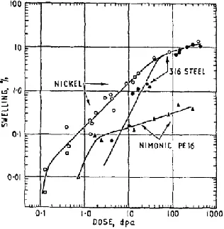
Figure 2.20 Void swelling percentage as a function of dose in nickel, 316 stainless steel and Nimonic PE16 (Ni-Co based) super alloy, irradiated with carbon ions at 525ºC [74].
Figure 2.21 Void swelling percentage as a function of temperature (T/Tm) in
molybdenum and nickel. Solid dots show neutron irradiation (>0.1 MeV) with a fluence of 5×10²⁰ n/cm2 (Mo) and 2.3×10²⁰ n/cm2 (Ni). Open circlus show neutron irradiation (>0.1
The occurrence of the void formation is usually limited in the temperature range of 0.3-0.6 Tm, above Stage V recovery. A typical temperature-dependent swelling curve of
swelling can be shown in Figure 2.21[74]. At such temperature, the mobility of vacancies or their clusters are high enough to accumulate and grow a void. But when temperature is higher than 0.6 Tm, cavities will appear thermally unstable and could undergo shrinkage via vacancy
emission from its surface.
Although different materials have similar trend of void swelling behavior as shown in Figure 2.20 and Figure 2.21, their detailed cavity growth process and swelling resistance is found complex and dynamic[129, 130], influenced by defect production, temperature, crystal structure, crystal anisotropy, and the density of crystalline defects such as dislocations and grain boundaries[54, 56, 74, 108, 131-136]. Dislocations, in particular, are believed to play an important role in promoting the cavity formation and evolution, since they act as stronger sinks for self-interstitial atoms than for vacancies, known as dislocation bias [137]. An example can be shown is that the cold-worked metals with high density of dislocation networks have less void swelling after irradiation[138-140].
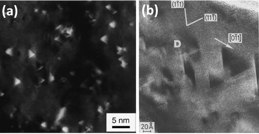
are typically observed in these metals nearby the c-component loops. For Mg, polyhedron shaped cavities are also observed in a commercial purity Mg under neutron irradiation similar to that of Zr and Ti in an early study. However, little is known for the relationship between the cavities and c-component SIAs loops in Mg so far.
Figure 2.22 Cavity formation in sponge Zr under 1MeV electron irradiation at 573K[46]. (a) nucleated voids in thin plate-like shape, followed by (b) void thickening, (c)
void length shrinkage at high dose.
direction perpendicular to it. It is believed that such evolution process might be attributed to the diffusion anisotropy difference (DAD) of the point defects in Zr, where net vacancy flux will go to the broad side of the void ((0001) facet) while net interstitial atoms flux will go to the side-walls. Although DAD model might help understand the evolution of voids to an equiaxed shape in their later stage of growth[53], it contradicts the observation that the nuclei can form a plate-like shape first at the very beginning. Due to the resolution limit in these studies, it still lacks of experimental details of how the cavity evolution process of Zr could occur, particularly at its beginning of the growth stage.
2.2.3 In-situ observation of defects interaction by TEM
In-situ observation directly reveals the mechanism of defect interaction and its corresponding microstructure change during the irradiation condition, which has attracted many attentions these years. There are two ways that such study can be conducted.
tall as three floors. Such large size and energy consuming will largely increase its maintenance cost, which is a big issue in the budget cut period. Actually, only few national laboratories or institutions around the world have these HVTEM, making such in-situ observation very difficult.
Figure 2.23 Overview of JEOL ARM-1300S high-voltage transmission electron microscope[146].
seen in Figure 2.24. The benefits from such ion irradiation configuration lie in not only the cost reduction, but also its ability to produce damage cascade in the microstructure, which is more close to the real nuclear reactor condition. These TEMs are very valuable but rare in the world. There are only 10 dual beam TEMs installed in the world, and two are located in the U.S. [153].
So far, in-situ observation by TEM has been demonstrated to be a fruitful method to reveal the mechanisms that govern the defects evolution under the irradiation. Utilizing high voltage electron or dual beam irradiation, the dislocation loops nucleation, growth and interaction[38, 48, 145, 154-157], void growth and shrinkage[13, 70, 141, 151, 158-163], the interaction between dislocation and SFTs/voids[97, 141, 164-168] have been successfully observed.
Although many attempts have been made to observe void formation in-situ [46, 169, 170], no atomic-scale observation of void nucleation and growth has been reported due to experimental difficulties. Since voids formation and growth are largely correlated to the diffusion process of point defects at void surface, the lack of understanding of void formation behavior at the atomic scale has adversely affected the development of advanced theoretical models to predict void evolution under irradiation. In this dissertation study, I choose Mg as a model material to perform the in-situ observation for void formation. The displacement threshold of Mg for electron is about 100 keV, which makes it possible to observe void nucleation and growth directly in a commercial 200 kV high resolution TEM without necessarily using dedicated TEM facilities. Details of the interesting observations using this technique will be given in Chapter 4 and 5.
2.3Oxide dispersion strengthened (ODS) alloys and their nanostructured features Nuclear energy is one of the few energy sources that could provide economical electricity to large power grids without emitting global warming CO2[1, 171]. Currently,
neutron doses (10-150 dpa) and longer service lifetime of the nuclear materials are also needed for Generation-IV reactors [3]. This requires nuclear materials to maintain acceptable irradiation and corrosion resistance as well as excellent thermal stability against thermal and irradiation creep, void swelling, irradiation hardening or embrittlement.
The oxide dispersion strengthened (ODS) alloy becomes one of the promising candidates for such applications, since it shows excellent high temperature strength and creep properties as well as good radiation resistance in terms of swelling and radiation embrittlement [173, 174]. Such good properties are majorly attributed to the dispersion of nanosize Yi-T-O enriched particles in the microstructure. In the following sections, the details of materials processing and its resultant nano structure feature will be introduced.
2.3.1 Synthesis of ODS alloys
Typical ODS alloys contain 9-20 wt.% Cr, 1-3 wt.% W, 0.2-1 wt.% Ti, 0.2-0.5 wt% Y2O3 and Fe in balance. Specifically, Cr element is added to provide the corrosion resistance
of ferritic matrix. W element offers solution hardening and creep strengthening with little detrimental embrittlement risk by Laves phase precipitations [175, 176]. The titanium addition allows an effective refinement of the nanoparticles due to the formation of complex Y-Ti-O enriched oxide particles [177-186]. Note that the Ti content is usually limited to less than 0.5 wt.% to prevent the formation of large TiO2 particles [187]. Similar to Ti, other
ODS alloys are made via the powder metallurgy, including mechanical alloying, hot consolidation, annealing, and thermal mechanical treatment [190-192]. Typically, the raw metal powders of about 10-100μm are ball milled with 20-nm Y2O3 powder in an attritor mill
for 48 hours in a dry Ar protection environment to produce non-equilibrium solid solution. Note that recent studies also showed that the μm Y2O3 powder addition could also produce
ODS alloy microstructure which is comparable to that of nano-size Y2O3 oxide
additions[193]. The as-milled powders will be first canned and degassed under vacuum at the temperature of 650-850ºC before consolidation by hot isostatic pressing (HIPing) or hot extrusion at about 850-1150ºC, producing high density of solid (~≥98%). The densified alloys will be further thermo-mechanical treated to achieve the desire mechanical properties. A summary of the optimized manufacturing route for ODS reduced activation ferritic (RAF) alloys was provided by Oksiuta et al. as shown in Figure 2.25 [187].
2.3.2 Y-Ti-O enriched nano-size oxide
The formed of Yi-Ti-O enriched particles are found to be most critical nanostructured features for ODS alloys since they could provide dispersion hardening effect and increase the mechanical and creep strength [179]. In addition, the presence of these oxide particles enhance the irradiation resistance of ODS alloys [194-196]. The beneficial irradiation resistance is largely due to the large volume fraction of boundaries that these oxide particles create. It is known that grain boundary area could promote the recombination of vacancies and interstitials from the irradiation, and larger grain boundary area could result in better irradiation resistance for the material. For instance, the defect density in ion-irradiated nanocrystalline Pd and ZrO2 is reported to be reduced by a factor of 3-4, when their average
grain sizes are reduced from 100 nm to 40 nm [197]. In addition, the interface of these Y-Ti-O enriched oxides and the matrix are also found to be strong sink source of He so as to preferentially absorb He and prevent them from precipitation in the matrix [194, 198].
The heat treatment temperature and the Y2O3/Ti ratio are found to be the two key
factors in forming dispersed oxides. Cayron et al. systematically investigated the temperature influence on the Yi-Ti-O nanoparticle formation in the microstructure [199], as summarized in Table 2.7. In addition, the microstructure evolution with temperature change is also shown. It is found that the Y2O3 particles are dissolved in the matrix in the as-milled powder, and no
![Table 2.1 Threshold displacement energy of varies kinds of materials [8, 16, 17]](https://thumb-us.123doks.com/thumbv2/123dok_us/1766223.1227183/30.612.179.450.240.671/table-threshold-displacement-energy-varies-kinds-materials.webp)

![Table 2.2 Formation and migration energy of vacancy in metals [8, 16]](https://thumb-us.123doks.com/thumbv2/123dok_us/1766223.1227183/33.612.151.480.155.507/table-formation-migration-energy-vacancy-metals.webp)

![Table 2.3 Formation energy of self-interstitials at different sites in hcp crystals [26]](https://thumb-us.123doks.com/thumbv2/123dok_us/1766223.1227183/36.612.123.520.331.597/table-formation-energy-self-interstitials-different-sites-crystals.webp)
![Figure 2.7 Illustration of Crowdion configuration in fcc crystal along [110] direction](https://thumb-us.123doks.com/thumbv2/123dok_us/1766223.1227183/38.612.231.418.124.311/figure-illustration-crowdion-configuration-fcc-crystal-direction.webp)