INTEGRATION METHODS FOR ENHANCED TRAPPING AND SPECTROSCOPY IN OPTOFLUIDICS
Praveen Cheriyan Ashok
A Thesis Submitted for the Degree of PhD at the
University of St. Andrews
2012
Full metadata for this item is available in Research@StAndrews:FullText
at:
http://research-repository.st-andrews.ac.uk/
Please use this identifier to cite or link to this item:
http://hdl.handle.net/10023/2546
Integration Methods for Enhanced Trapping and
Spectroscopy in Optofluidics
Praveen Cheriyan Ashok
This thesis is submitted for the degree of Doctor of Philosophy at the
University of St Andrews
Optical Manipulation & Microphotonics Groups
School of Physics & Astronomy
University of St Andrews
Dedicated to:
Love of my life, Bavishna,
My dear parents and beloved sister
n e n k e n
Integration Methods for Enhanced Trapping and
Spectroscopy in Optofluidics
Praveen Cheriyan Ashok
Abstract
“Lab on a Chip” technologies have revolutionized the field of bio-chemical analytics. The crucial role of optical techniques in this revolution resulted in the emergence of a field by itself, which is popularly termed as “optofluidics”. The miniaturization and integration of the optical parts in the majority of optofluidic devices however still remains a technical challenge. The works described in this thesis focuses on developing integration methods to combine various optical techniques with microfluidics in an alignment-free geometry, which could lead to the development of portable analytical devices, suitable for field applications.
The integration approach was applied to implement an alignment-free optofluidic chip for optical chromatography; a passive optical fractionation technique fractionation for cells or colloids. This system was realized by embedding large mode area photonic crystal fiber into a microfluidic chip to achieve on-chip laser beam delivery. Another study on passive sorting envisages an optofluidic device for passive sorting of cells using an optical potential energy landscape, generated using an acousto-optic deflector based optical trapping system.
On the analytical side, an optofluidic chip with fiber based microfluidic Raman spectroscopy was realized for bio-chemical analysis. A completely alignment-free optofluidic device was realized for rapid bio-chemical analysis in the first generation by embedding a novel split Raman probe into a microfluidic chip. The second generation development of this approach enabled further miniaturization into true microfluidic dimensions through a technique, termed Waveguide Confined Raman Spectroscopy (WCRS). The abilities of WCRS for online process monitoring in a microreactor and for probing microdroplets were explored. Further enhanced detection sensitivity of WCRS with the implementation of wavelength modulation based fluorescent suppression technique was demonstrated. WCRS based microfluidic devices can be an optofluidic analogue to fiber Raman probes when it comes to bio-chemical analysis. This allows faster chemical analysis with reduced required sample volume, without any special sample preparation stage which was demonstrated by analyzing and classifying various brands of Scotch whiskies using this device. The results from this study also show that, along with Raman spectroscopic information, WCRS picks up the fluorescence information as well, which might enhance the classification efficiency.
Declaration
1. Candidate’s declarations:
I, Praveen Cheriyan Ashok, hereby certify that this thesis, which is approximately 45000 words in
length, has been written by me, that it is the record of work carried out by me and that it has not
been submitted in any previous application for a higher degree.
I was admitted as a research student in September 2008 and as a candidate for the degree of
Doctor of Philosophy in Physics in September 2008; the higher study for which this is a record
was carried out in the University of St Andrews between 2008 and 2011.
Date …… signature of candidate ………
2. Supervisor’s declaration:
I hereby certify that the candidate has fulfilled the conditions of the Resolution and Regulations
appropriate for the degree of Doctor of Philosophy in the University of St Andrews and that the
candidate is qualified to submit this thesis in application for that degree.
Date …… signature of supervisor ………
3. Permission for electronic publication: (to be signed by both candidate and supervisor)
In submitting this thesis to the University of St Andrews I understand that I am giving permission
for it to be made available for use in accordance with the regulations of the University Library for
the time being in force, subject to any copyright vested in the work not being affected thereby. I
also understand that the title and the abstract will be published, and that a copy of the work may
be made and supplied to any bona fide library or research worker, that my thesis will be
electronically accessible for personal or research use unless exempt by award of an embargo as
requested below, and that the library has the right to migrate my thesis into new electronic forms
as required to ensure continued access to the thesis. I have obtained any third-party copyright
permissions that may be required in order to allow such access and migration, or have
requested the appropriate embargo below.
The following is an agreed request by candidate and supervisor regarding the electronic
publication of this thesis: Access to printed copy and electronic publication of thesis through the
University of St Andrews.
Acknowledgements
The first and foremost person to be acknowledged would be my supervisor, Prof. Kishan Dholakia for giving me this opportunity to do research under his guidance in the optical manipulation group. He was a constant source of inspiration and encouragement throughout my PhD studies. He gave me enough freedom and supported me throughout all the research and academic endeavors I have taken during these years which helped me to expand my skills and experiences. Special thanks to my second supervisor, Prof. Thomas Krauss for the opportunity he gave to work in his group and his constant support through discussions and suggestions. I would also like to express my thanks to Prof. Frank Gunn-Moore for the help and support he has given me during these years.
In the last three years I had the opportunity to collaborate and work with several outstanding researchers, to whom I would like to express my special thanks and gratitude. Robert Marchington is a person who has given me all support from the very beginning of my PhD studies. He has spent a considerable amount of time to train me on fabrication methods and to discuss various aspects of my research activities. A very special thanks to him for all the support he has given me throughout these years. Another person who has influenced my research was Gajendra Pratap Singh, who introduced me to the world of Raman spectroscopy. I would also like to express my gratitude to Tomas Cizmar, who spent his valuable time giving me training in new technologies. I have enjoyed working with Nan Ma, David Stevenson, Helen Rendall, Mark Scullion and Heather Dalgarno. Without mentioning names I would like to express my gratitude to all my colleagues in the group for their friendship which made my life enjoyable for last three years.
A special thanks to Robert Marchington, Heather Dalgarno, Prof. Frank Gunn-Moore and Christopher Reardon, who helped me to polish the content of this thesis by proof reading and suggesting corrections.
I should express special gratitude to Bavishna Balagopal, who is my colleague as well as my lovely wife. She has always supported me and encouraged me for all my endeavors. Thanks to Bavi, for filling my professional and personal life with loads of happiness.
Publications
Peer reviewed journals
• Ashok PC, Marchington RF, Mthunzi P, Krauss TF, Dholakia K (2010) Optical
chromatography using a photonic crystal fiber with on-chip fluorescence excitation. Opt Express 18 (6):6396-6407
• Ashok PC, Singh GP, Tan KM, Dholakia K (2010) Fiber probe based
microfluidic raman spectroscopy. Opt Express 18 (8):7642-7649
• Ma N, Ashok PC, Stevenson DJ, Gunn-Moore FJ, Dholakia K (2010) Integrated optical transfection system using a microlens fiber combined with microfluidic gene delivery. Biomed Opt Express 1 (2):694-705. doi:10.1364/BOE.1.000694
• Ashok PC, Singh GP, Rendall HA, Krauss TF, Dholakia K (2011) Waveguide
confined Raman spectroscopy for microfluidic interrogation. Lab Chip 11 (7):1262 - 1270. doi:10.1039/c0lc00462f
• Ashok PC, Luca ACD, Mazilu M, Dholakia K (2011) Enhanced bioanalyte
detection in waveguide confined Raman spectroscopy using modulation techniques. J Biophot 4 (7-8):514-518. doi:10.1002/jbio.201000107
• Čižmár T, Dalgarno HIC, Ashok PC, Gunn-Moore FJ, Dholakia K (2011) Interference-free superposition of non-zero order light modes: Functionalized optical landscapes. Appl Phys Lett. doi:10.1063/1.3552202
• Čižmár T, Dalgarno HIC, Ashok PC, Gunn-Moore FJ, Dholakia K (2011) Optical aberration compensation in a multiplexed optical trapping system. Journal of Optics 13 (4):044008. doi:10.1088/2040-8978/13/4/044008
• James TD, Scullion MG, Ashok PC, Di Falco AD, Dholakia K, Krauss TF (2011) Valve controlled fluorescence detection system for remote sensing applications. Microfluidics and Nanofluidics: 1-8. doi:10.1007/s10404-011-0818-1
• Ashok PC, Praveen BB, Dholakia K (2011) Near infrared spectroscopic analysis
• Ashok PC, Dholakia K (2011) Optical trapping for analytical biotechnology.
Curr Opin Biotech. doi:10.1016/j.copbio.2011.11.011 (Review paper)
Book Chapter
• Ashok PC, Dholakia K (under review) Microfluidic Raman spectroscopy for
bio-chemical sensing and analysis. In: Fritzsche W, Popp J (eds) Springer series on chemical sensors and biosensors: Optical nano- and microsystems for bioanalytics. Springer,
Patents
• Application: The University of St. Andrews Ashok PC, Singh GP, Dholakia K, “Filterless Fiber Probe Based Microfluidic Raman Spectroscopy”, International Patent Application No. PCT/GB2011/001406
• Application: The University of St. Andrews, Ashok PC, Singh GP, Dholakia K, Tan KM “Fiber-based microfluidic Raman spectroscopy” Application No. US 12/892,640, CA 2,715,886.
• Application: The University of St. Andrews, Ma N, Ashok PC, Stevenson DJ, Dholakia K, Gunn-Moore FJ, “ Microlensed fiber based poration” PCT/GB2011/000881
• Application: The University of St. Andrews, Marchington RF, Ashok P, Dholakia K., “Optical Trap”, WO/2010/007371 A2
Conference Publications
• Ashok PC, Marchington RF, Mazilu M, Krauss TF, Dholakia K Towards
integrated optical chromatography using photonic crystal fiber. In: Dholakia K, Spalding CG (eds), 2009. SPIE, p 74000R (Oral Presentation)
• Ashok PC, Singh GP, Tan KM, Dholakia K (2010) Microfluidic raman
spectroscopy for bioanalyte detection Paper presented at the International Conference on Raman Spectroscopy, Boston, US. (Poster presentation)
• Singh GP, Tan KM, Ashok PC, Herrington CS, Sibbett W, Brown CTA (2010) Surgical raman forceps for disease diagnosis. Paper presented at the International Conference on Raman Spectroscopy, Boston, US,
• Ashok PC, Singh GP, Luca ACD, Mazilu M, Dholakia K (2010) Embedded
fiber probes for raman spectroscopic detection in microfluidics. Paper presented at the Photonics 2010, Guwahati, India, (Oral Presentation)
• Ma N, Ashok PC, Gunn-Moore FJ, Dholakia K Fabrication of polymer microlens at the apex of optical fiber. In, 2010. vol 1. SPIE, p 817314 (Oral presentation)
• Cizmar T, Mazilu M, Dalgarno H, Ashok P, Gunn-Moore F, Dholakia K Optical sculpting: Trapping through disorder and transfer of orbital angular momentum. In: Andrews DL, Galvez EJ, Gluckstad J (eds), San Francisco, California, USA, 2011. SPIE, pp 79500R-79507
• Ashok PC, Dholakia K (2011) Integration methods for raman spectroscopy and
passive sorting in optofluidics. Paper presented at the Frontiers in Optics, San Jose, US, (Invited Talk)
• Ashok PC, Dholakia K (2011) Passive fractionation of colloids and cells using
List of Abbreviations
CAD Computer Aided Design CHO-K1 Chinese Hamster Ovary cells DA-AOD Dual Axis-Acousto Optic Deflector DAQ data acquisition
DFS digital frequency synthesizer DHM Digital Holographic Microscopy EOF electroosmotic flow
FACS fluorescence activated cell sorting FCS fetal calf serum
FIFO first in first out
FRET fluorescence resonance energy transfer
fs Femtosecond
GVD Group Velocity Dispersion HEK-293 Human Embryonic Kidney Cells
HF Hydrogen Fluoride
HWP half wave plate
impf iterative modified polynomial fitting
IPA isopropanol
IR Infra-Red
LMA PCF Large Mode Area Photonic Crystal Fiber
LoC Lab on a Chip
ND Neutral Density
NEC Noise Equivalent Concentration OCT Optical Coherence Tomography
OH hydroxyl
PBS polarizing beam splitter PC Principle Component
PCA Principle Component Analysis PCF Photonic Crystal Fiber
PDMS polydimethylsiloxane PLS Partial Least Square
RACS Raman activated cell sorting RBC red blood cells
RMSEP root mean square error of prediction rpm revolutions per minute
SERRS Surface Enhanced Resonance Raman Spectroscopy SERS Surface Enhanced Raman Spectroscopy
SNR Signal to Noise Ratio SPM Self-Phase Modulation TNT trinitrotoluene
TR3 time resolved resonance Raman spectroscopy
UV ultraviolet
Table of Contents
Abstract ... iv
Declaration ... v
Acknowledgements ... vi
Publications ... viii
Peer reviewed journals ... viii
Book Chapter ... ix
Patents ... ix
Conference Publications ... ix
List of Abbreviations ... xi
Table of Contents ... xiii
1. Introduction ... 1
2. Microfluidics – Physics & Fabrication Techniques ... 4
2.1 Introduction ... 4
2.2 Fluid dynamics at low Reynolds number ... 5
2.3 Microfabrication using soft-lithography ... 7
2.3.1 Design of the mask ... 9
2.3.2 Fabrication of the master mold ... 9
2.3.3 Fabrication of PDMS chip using soft-lithography ... 12
2.4 Embedding fiber into a PDMS microfluidic chip ... 15
2.5 PDMS membrane based microfluidic fabrication ... 17
2.6 Microfluidic channels with optical windows on both sides ... 17
2.7 Paraffin microvalve ... 19
2.8 Conclusion ... 21
Relevant publications ... 22
3. Integrated optical chromatography using photonic crystal fiber ... 23
3.1 Introduction ... 23
3.2 Theory of optical chromatography ... 25
3.3 History of optical chromatography ... 27
3.4 Optical Chromatography with on-chip light delivery – Rationale ... 31
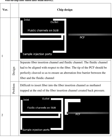
3.5 Design of optical chromatography chip with on-chip fiber light delivery ... 32
3.5.1 Choice of the fiber – Large Mode Area Photonic Crystal Fiber (LMA-PCF) ... 32
3.5.2 Chip design and fabrication ... 34
3.6 Optical setup... 39
3.7 Fluidic setup ... 41
3.8 Calibration of the system ... 42
3.9 On-chip fluorescence excitation ... 45
3.10 Verification of the purity of spatially separated samples ... 46
3.11 Separation of mammalian cells incubated with polystyrene beads ... 47
3.12 Conclusion ... 49
Relevant Publications ... 51
Patent ... 51
Contributions ... 51
4. Towards passive optical cell sorting in an optofluidic chip using optical landscapes52 4.1 Introduction ... 52
4.2 Optical trapping system with a DA- AOD – optical design and interface ... 53
4.2.1 DA-AOD controller ... 56
4.2.2 LabVIEW interface ... 57
4.3 Theory of optical landscape sorting using a line trap ... 58
4.4 In-situ calibration for optimizing parameters for sorting cells... 61
4.5 Conclusion ... 65
5. Fiber probe based microfluidic Raman spectroscopy ... 68
5.1 Introduction ... 68
5.2 Raman spectroscopy... 69
5.3 History of microfluidic Raman spectroscopy ... 71
5.3.1 Initial studies ... 72
5.3.2 Raman spectroscopy to probe reactions ... 73
5.3.3 Bio-chemical detection using SERS microfluidics ... 74
5.3.4 Raman spectroscopic probing of microdroplets ... 75
5.3.5 Microfluidic Raman spectroscopy in cell science ... 76
5.3.6 Recent Developments... 77
5.4 Fiber probe based microfluidic Raman spectroscopy – Rationale ... 78
5.5 Design of the split Raman probe ... 80
5.6 Chip design and fabrication ... 82
5.7 Detection device ... 83
5.8 Optimizing the collection geometry ... 84
5.9 Detection limit of the microfluidic device with the embedded probe ... 86
5.10 Effect of flow ... 88
5.11 Residual free nature of the chip ... 88
5.12 Conclusions ... 89
Relevant publications ... 90
Patent ... 91
Publicity ... 91
Contribution ... 91
6. Waveguide Confined Raman Spectroscopy (WCRS) ... 92
6.1 Introduction ... 92
6.2 Embedding fiber into the microfluidic chip ... 94
6.4 Characterization of the device ... 95
6.4.1 The effect of collection angle ... 97
6.4.2 The effect of fiber length... 98
6.4.3 The effect of fiber core size ... 99
6.5 Minimum detection limit for urea ... 100
6.6 Monitoring of micro-reaction in a micro-reactor ... 101
6.7 Detection of microdroplets using WCRS ... 105
6.8 Conclusion ... 107
Relevant publications ... 108
Patent ... 109
Publicity ... 109
Contribution ... 109
7. Enhanced bioanalyte detection in waveguide confined Raman spectroscopy using wavelength modulation ... 110
7.1 Introduction ... 110
7.2 Wavelength modulation implemented in a WCRS device ... 110
7.3 Raman acquisition method ... 112
7.4 Detection sensitivity ... 112
7.5 Conclusion ... 115
Relevant publications ... 116
Contributions ... 116
8. Near infrared spectroscopic analysis of single malt scotch whisky in an optofluidic chip ... 117
8.1 Introduction ... 117
8.2 Experimental ... 119
8.3 Results and discussions ... 121
8.3.1 Concentration estimation ... 122
8.3.3 Effect of photo-bleaching ... 127
8.3.4 Reproducibility ... 129
8.4 Conclusion ... 130
Relevant publications ... 131
Publicity ... 131
Contributions ... 131
9. Fabrication of microlens fiber combined with microfluidic gene delivery for integrated optical transfection ... 132
9.1 Introduction ... 132
9.2 Fabrication of microlens tipped fiber ... 134
9.3 Characterization and modeling of the microstick ... 138
9.4 Fabrication and characterization of collimating microlens ... 140
9.5 Cell transfection using microlens fiber ... 142
9.6 Design of a wholly integrated system for localized drug delivery... 144
9.7 Efficiency of optical transfection ... 146
9.8 Conclusion ... 148
Relevant publications ... 149
Patent ... 149
Contributions ... 150
10.Conclusions & Future Outlook ... 151
10.1 Summary of the thesis ... 151
10.2 Future outlook ... 155
10.2.1 Optical chromatography ... 156
10.2.2 Periodic optical landscape based passive optical cell sorting ... 156
10.2.3 WCRS 157 10.2.4 Polymer microlensed fiber fabrication ... 158
Appendix 1 – Cell Preparation Protocols for the Optical Chromatography Experiments
... 159
Protocol for the photo-transfection of HEK-293 cells ... 159
Protocol for the incubation of HEK-293 cells with microspheres ... 159
1.
Introduction
The advancements in microfluidics technologies have revolutionized the field of bio-chemical analytics. Optical technologies have played a crucial role in realizing the dream of implementing “Lab on a Chip (LoC)”. Hence the term “optofluidics” has emerged in recent years to address technologies where optical techniques are used on a microfluidic platform to obtain desired functionality. While optical techniques such as imaging and spectroscopy may be used to probe the sample in the microfluidic channel, the use of optical micromanipulation allowed manipulation of microscopic particles within the microfluidic channel.
The majority of such technologies have further room for improvement in terms of the miniaturization and integration of the optical systems to achieve truly portable devices, suitable for field applications. This thesis mainly focuses on these aspects developing optofluidic technologies for enhanced sorting and bio-chemical analysis with special emphasize upon integration or embedding optical components within the microfluidic chip to make it alignment-free and portable. Although there is this common theme for the studies described in this thesis, they have diverse fields of application. Hence, instead of general review chapters in the beginning of this thesis, a brief review within the areas of application is given at the beginning of each chapter. The studies described in this chapter can be mainly divided into three categories. Micro-fabrication techniques, which are detailed in chapter 2 and chapter 9, optofluidic cell sorting, which is described in chapter 3 and chapter 4 and optofluidic bio-chemical analytics using Raman spectroscopy, discussed in chapter 5 to chapter 8.
Chapter 2 discusses the basic physical principles that govern fluid dynamics at the microfluidic scale. Also this chapter explains in detail the soft lithographic fabrication protocol for microfluidic chip fabrication, along with minor modification to protocols, implemented to achieve integration of optical techniques to a microfluidic platform. The chapter also describes the implementation of a close-open paraffin microvalve which can be used for sensing applications.
achieve refractive index driven and size driven fractionation was demonstrated. Also optical chromatographic fractionation of the sample combined with on-chip fluorescent excitation was demonstrated by exploiting the endlessly single mode nature of PCF.
The work discussed in chapter 4 is a step towards implementing a microfluidic device to achieve passive cell sorting using optical landscape. The implementation of an acousto-optic deflector based optical tweezer system to create optical landscape is explained along with the details of the LabVIEW interface designed for this application. Further the basic theory behind fractionation of micro-particles using periodic optical landscape is discussed. A fundamental challenge in passive optical fractionation of cells using periodic optical landscape is the difficulty choosing the right sets of parameters due to the lack of knowledge of the absolute size or refractive index of the cellular samples. An in situ calibration method is proposed which can be used to find a spherical micro-bead with known size and refractive index whose interaction with flow and optical field is equivalent to that of a particular cellular species. This method offers the opportunity to assess the feasibility of fractionating two types of cells and helps to choose the right set of parameters for successful fractionation of cells.
analysis. Classification of Scotch whisky was achieved by implementing multivariate analytical techniques on the Raman spectra obtained using WCRS based microfluidic chip.
Chapter 9 revisits microfabrication techniques. This chapter discusses a novel fabrication protocol for the fabrication of polymer microlens at the tip of an optical fiber. This flexible and relatively inexpensive method was used to fabricate a microlensed fiber with which an integrated system was built to achieve optical transfection combined with localized gene delivery.
2.
Microfluidics – Physics & Fabrication Techniques
2.1
Introduction
The motivation behind the field of microfluidics, which is popularly addressed as ‘LoC’, is to miniaturize macroscopic analysis and synthesis modalities in chemistry and biology and integrate them into a single chip. The advancement of this technology aims to revolutionize the field of bio-chemical analytics through automation, akin to the revolution in computation through the advent of microelectronics[1]. The early 1990s saw the emergence of this new field with the introduction of gas chromatographic chips [2,3]. This approach offers so many advantages compared to conventional analysis methodologies using bulk fluidic systems, such as the small volume required for analysis, controlled interactions between materials at micrometer levels, and the unique behavior of liquids in the low Reynolds number regime. Though such devices were originally developed for applications in chemistry, today this technology finds its potential in much wider depth of fields. The past 15 years has seen the convergence of this technology within many disciplines including chemistry, physics, electronics and biology, hence expanding its scope vastly beyond its initial expectations [4].
When the physical dimensions of the fluidic channel are scaled down to the order of micrometers, the physics governing the fluid behavior differs from that of the macroscopic scale due to the low Reynolds number of the fluid. Hence fluids on the micrometer scale shows several interesting dynamics such as non-turbulent laminar flow which are counter-intuitive when compared to the dynamics of the fluidics in the macroscopic world [5]. While the absence of turbulence offers better control of the fluids within the microfluidic chip, it poses problems for applications where mixing of two fluid streams is desirable.
how to fabricate cheap and disposable chips to avoid cross contamination of samples. One desired micro-fabrication technology which offers these qualities is “Soft Lithography” which is based on a moulding approach which allows rapid prototyping and replica moulding of chips [7]. Even though there are a wide variety of techniques to choose from, soft-lithography based fabrication is still predominant in the research world, based on the number of publications in last 10 years [6]. The majority of the studies mentioned in this thesis use microfluidic chips fabricated using soft lithography. The following sections in this chapter contain a detailed description on various aspects of soft lithography based micro-fabrication.
2.2
Fluid dynamics at low Reynolds number
The dynamics of an incompressible Newtonian fluid can be represented using the Navier-Stokes equation, which is essentially the continuum form of Newton’s second law [1].
2
.
du
u
u
p
u
f
dt
ρ
+ ∇ = −∇ + ∇ +
η
[2.1]Where, u is the fluid velocity and t is time. The left hand side of the equation corresponds to the inertial acceleration terms where ρ is the density of the fluid. The right hand side corresponds to various forces that act on the fluid. The first term corresponds to the pressure gradient where p corresponds to the pressure. The second term corresponds to the viscous stress with η being the shear viscosity of the fluid. In special conditions, capillary stresses and effect of diffusion should be taken into consideration when calculating the viscous stress term. f is the body force density,
which corresponds to other additional external force components [1,8].
The Reynolds number (Re) is one of the most popular parameters in the list of the above mentioned dimensionless numbers for characterizing fluidic flow. This parameter determines the relative dominance of inertial to viscous forces [9].
0 0
Re
ρ
U L
η
=
[2.2]Where U0is the fluid velocity and L0is the characteristics length scale of the contained fluid [1]. The value of Reynolds number determines whether the fluid dynamics are laminar or turbulent. For low values of Reynolds number (typically Re<1), the viscous force will be predominant when compared to the inertial force. In this regime, the non-linear term in the left hand side of equation 2.1 can be neglected; resulting in a linear and simplified equation for Stokes flow. Such flow is called laminar flow. When Re>2000, the inertial forces play a predominant role in the fluid dynamics resulting in a turbulent flow. Hence the Reynolds number is a quantity that predicts whether fluid dynamics are laminar or turbulent [1].
In a low Reynolds number world, mixing of two fluid streams can occur only through diffusion as the fluid is non-turbulent. When compared to turbulent mixing and mixing through thermal convection, diffusion mixing is a slow process resulting in an extended timescale for complete mixing of two streams of fluids [1]. Depending upon the application this slow mixing dynamic can be an advantage or disadvantage. Hence while designing the microfluidic device, it is essential to know the length-scale in which two parallel laminar flows are mixed through diffusion. It is the Peclet number that gives the number of channel widths required for complete mixing of these two streams. For a microfluidic channel with square cross-section of widthw, the Peclet number (Pe) can be estimated for two parallel flowing fluids with diffusion coefficient D as:
0
U w
Pe
D
=
[2.3]the microfluidic device and the collection tank to which the fluid flows. By adjusting the height of the reservoir and collection tank, one can vary the flow velocity and this can result in a smooth flow. Another approach is to use a syringe pump to apply pressure. Even though commercially available syringe pumps can be used to achieve very low flow rates in the range of Pico liters per second, at these small flow velocities, due to mechanical instability of the pump, the flow is not smooth enough for microfluidic applications. Another limitation of the pressure driven flow is that the cross section of the flow velocity profile is not uniform. It follows a parabolic flow profile with maxi-mum velocity at the center [10]. An alternative approach is to use Electro-Osmotic Flow (EOF). In this, by applying an electric field across the fluidic channel, fluidic flow can be achieved. EOF offers a uniform flow profile. But implementing EOF is difficult as it significantly depends on the surface chemistry of the flow channel and on the buffer composition [10]. All the microfluidic experiments mentioned in this thesis have been performed using pressure driven flow using syringe pumps or rotary pumps which can achieve relatively low flow rates of the order of microliters/hour.
2.3
Microfabrication using soft-lithography
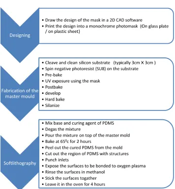
The majority of the microfluidic research detailed in this thesis used PDMS based soft lithography for fabrication of microfluidic devices. This section will detail various steps involved in fabrication of PDMS based microfluidic chips. A flow chart showing the general fabrication protocol is given in Fig. 1.
One of the advantages of a soft-lithography based fabrication technique is the ability for rapid prototyping. It is possible to translate a concept into a microfluidic chip within 1-2 days. Once the master mold is fabricated it is possible to fabricate 4-5 such chips per day.
[image:27.595.136.492.263.648.2]2.3.1 Design of the mask
The first stage of the procedure is the design of the mask to be used for UV-photolithography to fabricate the master mold. This is usually implemented using suitable 2D Computer Aided Design (CAD) software. A commercial software package - Elphy Plus (Raith) – was used for drawing the mask design. The drawn design can be produced on glass masks if high resolution is needed or can be printed on flexible plastic sheets (Microlithography services Ltd.), to obtain a monochrome photomask. Since negative photoresist is used for fabricating the master mold, the region where structures are to be retained are kept transparent in the photomask. While printing to plastic sheet is cheaper compared to the glass masks, the resolution that can be achieved by this is limited to ~20 µm, compared ~1 µm for the case of a glass mask.
2.3.2 Fabrication of the master mold
The next stage in the procedure is to fabricate the master mold which would be used to mold the structure to a silicon elastomer. Hence to achieve microfluidic channels which are the patterned relief structures on cured PDMS block, the master mold should have raised structures defined in photoresist [11]. A negative photoresist – SU8 (Polymicro Inc.) – was used for defining the structures in the master mold. The master mold was fabricated on a single side polished silicon wafer (IDB Technologies Ltd.). The silicon wafer was cleaved to desired size (typically rectangles with sides between 2 cm – 4 cm) and was rinsed in acetone, isopropanol (IPA) and de-ionized water. After drying with nitrogen, it is kept in an oven at a temperature of 180 0C for eight hours to ensure that the surface of the substrate is fully dehydrated to maximize adhesion in the next stage.
and SU8 2000.5 (low viscosity) were mixed in different ratios to produce photoresists with the desired viscosity. The thickness of the spun photoresist is governed by the empirical equation [13]:
2
kp t
w
= [2.4]
Where, pis the resist solid content percentage, which is a function of viscosity of the resist,w is the spinner speed in rpm/1000 and k is the spinner constant (typically 80-100) that depends on various physical parameters such as the size of the wafer, the humidity and the temperature of the environment. Although a calibration graph of spinning speed vs. film thickness was given by the manufacturer for standard SU8 resists with known viscosity, since the value of kis sensitive to the environment, calibration was required for fabrication of each mold depending on the specific conditions.
For spinning the flat layer of SU8, first a drop of photoresist was poured on top of the substrate, and by tilting the substrate the resist was allowed to flow and cover the whole surface of the substrate. The spinning of the resist was performed in three steps. In the first 15 seconds the substrate was spun at 500 revolutions per minute (rpm), which ensures spreading of the resist evenly over the whole surface area of the substrate. In the next 15 seconds the revolution speed would be increased to half of that of the final spinning speed. This allowed removal of any extra SU8 from the substrate. In the final stage the speed was increased to the actual desired speed and would spin for 30 s spreading the SU8 layer evenly resulting in a flat layer of SU8 on the surface of the silicon substrate. Although reducing the spinning speed would result in thicker films, it is not desirable to reduce the spinning speed below 1000 rpm as this would create unevenness of the final layer. For achieving higher thicknesses of the SU8 layer (~300 µm), a multi-layer spin coating of SU8 was possible by spinning multiple layers of SU8 after pre-baking each layer after spinning.
After the pre-bake, the substrate was allowed to cool for 10 minutes prior to UV exposure.
The next stage was UV photolithography, where the design on the printed mask is transferred to the SU8 layer by UV exposure. Since SU8 is a negative photoresist, the region which was exposed to UV would undergo a photochemical reaction resulting in cross-linking (polymerization) of the material. The required exposure times depend upon the thickness of the SU8 layer. While a low exposure time inhibits proper cross-linking, a high exposure time would result in a trapezoidal channel cross section instead of a rectangular one as the UV radiation leaks to the sides once the cross-linking process is completed in the actual exposed region. When using low resolution printed mask for UV photolithography, it is necessary to temporarily fix the mask onto a glass plate so as to keep the mask flat during the exposure. To temporarily bond the mask to a glass plate a drop of water was used as a bonding agent. A drop of water was placed onto a glass plate and the mask was then placed on top of the water droplet, sandwiching a thin layer of water between the glass substrate and the printed mask. The shear stress due to the surface tension of the water provides a temporary but strong bond between the glass and the printed mask. The UV exposure was performed on a mask aligner (Carl Zeiss) where the substrate with SU8 layer was kept as close as possible to the mask to avoid leaking of UV light through the edges of the mask during exposure.
Once UV exposure is complete the substrate was post-baked (post exposure baking) to complete the cross-linking process of SU8. This baking step was performed similar to that of pre-bake by warming up at 65 0C and then baking at 95 0C. The baking time is dictated by the thickness of the material (typically 1 minute at 65 0C and 10 minutes at 95 0C for an SU8 layer of thickness 80 µm). After post-baking, the structures defined by UV exposure would be visible on the substrate.
destruction of the structures may occur. Once the un-polymerised material was completely dissolved in EC solution, the substrate would be rinsed in IPA and purged with N2 gas for drying.
After completing the developing stage, the substrate was left in an oven at a temperature 180 0C for 4 hours for hard baking. Any minor cracks in the structure after developing would get fully cured during the hard baking procedure.
After the hard baking stage, the substrate was silanized to create a non-sticky layer on top of the substrate which would ease pealing up of cured PDMS during the soft lithography process. To silanize the substrate, trichlorosilane (Fluorochem) was deposited on the substrate through vapor deposition using a desiccator. A drop of trichlorosilane (~20 µl) was kept in the desiccator along with the substrate (keeping the surface with the structure facing up). Using a vacuum pump, the gas inside the desiccator was pumped out for 30 minutes, this causes the trichlorosilane to evaporate and become deposited on the substrate. This stage completes the fabrication of mold. The whole process of fabricating the master mold was performed in a class 10,000 clean room facility.
2.3.3 Fabrication of PDMS chip using soft-lithography
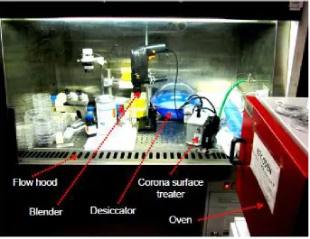
The next stage is to fabricate PDMS chips from the master mold using a stamping and molding procedure. A soft-lithography workstation outside the cleanroom was used for this stage of fabrication. The workstation as shown in Fig. 2 consists of a flow hood containing facilities for preparing the PDMS mixture and processing the cured PDMS to make the microfluidic chips. The workstation also has an oven kept at 65 0C to cure the PDMS.
degassed, it was poured on top of the mold which was kept inside a Petri dish (90 mm diameter). The volume of mixture poured into the petri-dish typically varies between 20 mL to 30 mL depending on the desired final thickness of the PDMS chip (typically 2 mm to 5 mm). The mixture had to be poured with special care to avoid any bubble being trapped within the fluid. Any bubbles seen after pouring the mixture into the Petri dish are removed using a pipette or syringe.
Fig. 2: Photograph of the lithography workstation. All instruments required for the soft-lithography fabrication was setup inside a flow hood to protect the sample from dust. A homemade blender, built using a commercially available driller was used for mixing PDMS. Desiccator was used for degasing the mixed PDMS. A corona surface treater was used for treating the cured PDMS surface with oxygen plasma prior to permanent surface bonding. An oven kept at 65 0C was used for curing the PDMS.
PDMS can be cured in a wide range of temperatures ranging from room temperature to 200 0C. With higher curing temperature the curing process is faster. PDMS was cured in an oven with a relatively low curing rate at 65 0C for two hours, which ensured uniform curing for the whole volume and provided enough time for any trapped air bubbles to escape from the PDMS.
create inlet and outlet ports. These were punched using a micro-punch (Harris) depending on the diameter of the tubing to be used for the microfluidic experiment (typically 1.2 mm or 2 mm diameter). Typically the diameter of the inlet was kept slightly below the diameter of the tube to be attached. Due to the elastic nature of the PDMS material, this will allow insertion of the tubing into the inlets and would ensure an automatic sealing which would be reversible.
The next stage is to bond the PDMS block with relief structures to a substrate, which can be either a microscopic slide or a flat block of PDMS. There are mainly two types of bonding possible, temporary and permanent. In temporary bonding, the surfaces to be bonded were brought together and the Van der Waals force would hold them together. Such bonds are suitable for experiments where the microfluidic flow was achieved only through negative pressure created by suction. This type of bonding is reversible. Permanent bonding is stronger and irreversible which could withstand positive pressure inside the microfluidic channel. To achieve the permanent bonding, the surfaces to be bonded were treated with oxygen plasma using a corona surface treater (Electro Technic Products, Inc.) for 4 seconds each, which temporarily ionizes the surfaces. The surfaces were then rinsed with methanol (Sigma Aldrich) and brought into contact to be bonded. Rinsing with methanol allowed the surface to remain ionized for a longer period of time, without this process the surfaces would be neutralized within one minute after exposure to the oxygen plasma. Methanol acts as a lubricant, which helps to slide one surface on top of another to position it properly. Methanol would evaporate relatively quickly allowing the surfaces to bond. After bonding the two surfaces together, the chip would be left inside a 65 0C oven for eight hours to ensure that the surfaces are bonded properly. The chip would be ready to use after eight hours.
2.4
Embedding fiber into a PDMS microfluidic chip
Optical detection techniques have played a crucial role in the advancement of the field of LoC [14]. However delivering and collecting optical signals in microfluidic chips still remains as a challenge for which several solutions are being proposed by the research community. One of these solutions is to develop LoC devices where all the optical components such as source and detector are integrated into the microfluidic chip [15]. Another approach is to use integrated [16] or embedded [17] waveguides to create optical paths to microfluidic chips.
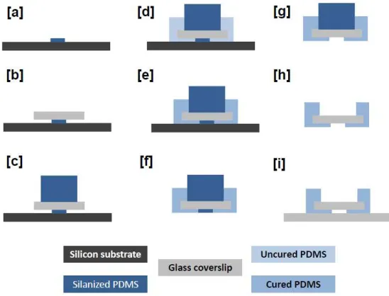
The latter approach is often realized by embedding an optical fiber into pre-defined fiber insertion channels. The realization of such pre-defined fiber insertion channels using soft-lithography based fabrication techniques is not trivial, as the shape of the microfluidic channel that can be fabricated is limited only to a rectangular cross section because of the photolithographic fabrication of master mold. A novel fabrication protocol was implemented to achieve pre-defined fiber insertion channel with circular cross section in PDMS. This has been realized by fixing a piece of fiber, which has same dimension as that of the optical fiber that is to be inserted into the chip, on the master mold. Fig. 3 shows a comparison between microfluidic channels with rectangular cross section, defined by SU8 structures using the conventional photolithographic fabrication protocol and circular cross-section achieved by this modified protocol.
Fig. 3: [a] Rectangular microfluidic channel defined by SU8 structures in the mold. [b] Circular channel cross section in PDMS by fixing a piece of optical fiber on the master mold.
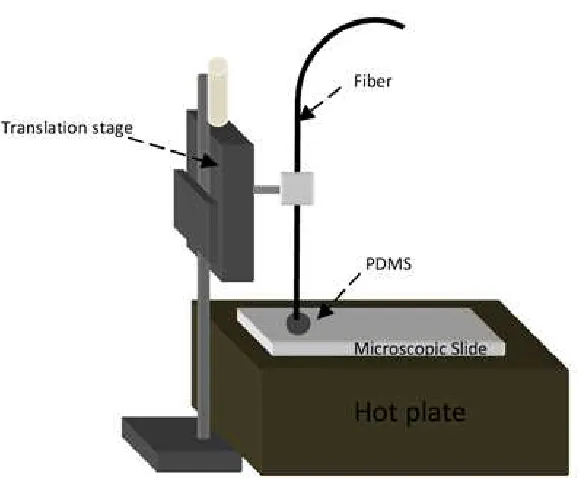
substrate. Subsequently the substrate was exposed to UV to cure the adhesive which would hold the piece of fiber to the substrate. However this approach would not be sufficient to fix fibers whose diameter is ~125 µm (diameter of standard single mode fibers). Adhesive just on the end would not be sufficient to hold fibers of this dimension. Also during the process of pealing PDMS from the mold, this will leave some PDMS lips on the fluidic channel. Hence to fix fibers of smaller diameter, SU8 was used as adhesive. A 5 µ m thick SU8 was spun on top of the silicon substrate. The fiber to be fixed was dropped on top of the thin SU8 layer. After pre-baking, the whole SU8 layer was flood exposed leaving a flat SU8 layer with the fiber stuck on this layer. The standard protocol was then followed to define other microfluidic channels on this substrate. As shown in Fig. 4[a], it was easy to join the circular cross section microfluidic channel defined by the fiber piece to the rectangular cross sectioned microfluidic channel defined by the SU8 structures. This was achieved by overlapping the rectangular structures to be defined on top of the fiber piece during UV exposure.
Since fiber pieces of the same dimension were used to define the fiber insertion channel, and as PDMS is elastic in nature, once the fiber was inserted into the PDMS chip, it ensured a leak-proof embedding of the fiber. To make the insertion of the fiber into this pre-defined fiber insertion channel easier, methanol was used as a lubricant within the fiber insertion channel, which easily evaporates within a few minutes after insertion and positioning of the fiber inside the microfluidic chip.
2.5
PDMS membrane based microfluidic fabrication
The soft-lithography based PDMS fabrication protocol detailed in section 2.3.3 is for fabricating microfluidic channels within PDMS blocks. For some specific applications such as implementation of microvalves mentioned in section 2.7 [18], membrane based PDMS fabrication would be desirable. Depending on the applications, PDMS membrane thicknesses can vary from 50 µm to 1 mm. The fabrication protocol varies depending on the desired thickness of the membrane.
To fabricate membranes with relatively low thickness (~50 µm), uncured PDMS was spun onto a flat glass or silicon substrate which had previously been silanized. The curing process was performed on a hotplate at 120 0C for 3 to 5 minutes. Once PDMS was cured, the membrane was carefully peeled out.
If a relatively thick (~800 µm to 1 mm) membrane was required and the actual specific thickness is not a concern, uncured PDMS was allowed to spread on a silanized flat substrate followed by a quick curing on a hotplate as mentioned in the previous method. To control the thickness of the membrane, uncured PDMS was sandwiched between two silanized substrates, keeping a spacer of desired thickness between the substrates. This ensured PDMS membrane which is flat on both sides and has a known thickness.
2.6
Microfluidic channels with optical windows on both sides
Optical access to microfluidic channels is always a major concern when designing optofluidic chips. When implementing techniques such as optical tweezers, which uses a high numerical aperture objective, within optofluidics, it is desirable to have an optically flat window of thickness ~100 µm to avoid aberrations on the optical beam delivered into the microfluidic channel. This is usually achieved by using a microscope coverslip as the substrate in the bottom of a PDMS microfluidic chip.
Even if the channel was fabricated using a PDMS membrane, to reduce the thickness of the material on top of the channel, the membrane would not be optically flat, leading to unnecessary aberrations.
[image:37.595.175.449.338.547.2]The solution is to embed a microscopic coverslip within a PDMS block. A protocol was developed to achieve this using a silanized PDMS membrane and a silanized PDMS block. This protocol can be implemented for relatively high (> 500 µm) and wide (> 1 mm) microfluidic channels. A PDMS membrane of thickness ~ 500 µ m was fabricated by sandwiching uncured PDMS between two substrates as detailed in section 2.5. After curing, the membrane was peeled out and cut into 1 cm x 1mm long strips. These strips were then silanized. These strips were used for defining the microfluidic channels on the mold. The fabrication protocol is detailed using the schematic diagram shown in Fig. 5.
2.7
Paraffin microvalve
Every microfluidic based sensor system requires a microvalve for controlled sample input. There are mainly two types of microvalve approaches – Active and Passive [20,21]. Passive microvalves generally act as a check valve to restrict the flow only in one direction, whereas active microvalves involve actuators for the valve operation. A simple paraffin based active microvalve was designed for a one time use sensor. In this case since the sensor is for one time use only, the valve required should be a single shot close-open valve. The final device had to be portable, hence the power consumption to open the valve should be kept as minimum as possible. Also the valve has to be compatible with PDMS based soft lithographic fabrication techniques.
Thermally actuated non-mechanical microvalves based on phase changing nature of paraffin wax have proved to be ideal for a low response time for opening which will result in less power consumption [22,23]. Also paraffin based microvalves tend to hold higher pressure compared to its closest counterparts [21]. In contrast to the work of Liu et al. [23], where the channel size was in the range of millimeters, the size of the channel for the chip used in this study was 250x50µm. This small dimension makes it difficult to load the wax into the channel to close the valve.
The microvalve was fabricated in a single layered PDMS membrane of thickness ~800µm, using conventional soft lithographic techniques [7]. To load the wax a wax loading channel crossing perpendicular to the fluidic channel was used as shown in Fig. 6.
Fig. 6: Design of the paraffin microvalve showing the main fluidic channel for the sample, microheater and wax loading channel. Wax is shown in grey and the sample fluid is shown in blue. The valve is in the “closed” position. When the heater is energised, the wax above it melts and allows fluid to flow from right to left. The excess wax is captured and resets in the “capture chamber” on the left.
[image:39.595.142.473.134.288.2]An aluminium based microheater fabricated on the coverslip to which the PDMS chip was fixed, acted as the actuator to open the paraffin based microvalve. The heater was positioned at the junction of wax channel and fluidic channel as shown in the diagram. The total length of the heater was 5mm. The width of the heater coil was 25µm and each turn of the coil was separated by a distance of 40 µm. The thickness of the microheater was between 100nm and 200nm.
Fig. 7: Microvalve actuation: The heating coil is aligned along the main fluidic channel. The larger channel is used to load the wax. (a) The valve in the closed position. (b) Current is applied, wax melts, and sample fluid flows. (c) Channel completely filled with sample fluid.
[image:39.595.108.528.485.596.2]2.8
Conclusion
This chapter details the background of the theory of microfluidics and basic fabrication techniques, which have been used for the research detailed in the following chapters. The soft lithography based fabrication protocol explained in 2.3 is the standard one. One of the focal points of the studies presented in this thesis is the means by which various optical techniques were incorporated into microfluidics to achieve optofluidic devices with enhanced functionalities and portability. This required modification of the standard soft-lithography protocols to achieve specialized functions. One of such modifications was to achieve pre-defined fiber insertion channels with circular cross-sections in PDMS. The technique where a fiber piece was incorporated into the master mold to achieve such a fiber insertion channel played a crucial role in developing various optofluidic devices for optical sorting and chemical sensing which are detailed in following chapters.
When designing microfluidic chips, to be integrated with free-space imaging devices such as biological microscopes, an important design consideration is to provide proper optical windows to probe the sample inside the microfluidic channel without the substrate causing optical aberrations. Conventional soft-lithographic techniques offer a means to provide such an optical window on one side of the channel by bonding the PDMS block to a microscope coverslip. However for some specific applications such as DHM based imaging of a sample in a microfluidic channel, optical access on two sides of the microfluidic channel may be necessary. This was achieved by a modified protocol using silanized PDMS membranes and PDMS blocks.
microfluidic sensor where multiple sensors would be embedded within one microfluidic chip.
Although a general overview of the fabrication protocol was presented in this chapter, modifications to this were used in designing and implementing various devices discussed in the following chapters. The specific fabrication protocol used for each project is explained in detail in respective chapters in later parts of this thesis.
Relevant publications
• Dharanipathy UP, Di Falco A, Scullion MG, Ashok PC, Marchington RF, Krauss TF (2009) An integrated slotted photonic crystal biosensor array. Paper presented at the EOS Topical Meeting on "Blue" Photonics - Optics in the Sea Aberdeen,
• James TD, Scullion MG, Ashok PC, Di Falco A, Dholakia K, Krauss TF (2011) Valve controlled fluorescence detection system for remote sensing applications. Microfluidics and Nanofluidics:1-8. doi:10.1007/s10404-011-0818-1
Contributions
3.
Integrated optical chromatography using photonic crystal fiber
3.1
Introduction
Optical chromatography is a simple and promising passive sorting technique, which utilizes the interplay between microfluidic drag force and the optical radiation force to achieve spatial separation of microparticles. When a particle in a microfluidic flow encounters a gently focused laser beam propagating coaxially in the opposite direction to the flow, the particle experiences a force against the flow due to the radiation pressure of the laser beam. The particle comes to a rest point where the optical forces are balanced by the Stokes’ viscous drag force. The distance of the rest point from the focus of the laser beam is referred to as the retention distance. The retention distance of the particle is dependent upon the size, refractive index and shape of the particle for a fixed laser beam power and fluid flow velocity which is explained mathematically in [24]. Optical chromatography has been applied to the separation of colloidal materials and to different species of biological particles [25]. Optical chromatography has also been used to study the in situ reaction rates in immunoassays [26]. The field of optical
chromatography is maturing with the capability for filtering out, concentrating and collecting a particular species from a mixture of particles for analysis [27].
The major limitations for the application of optical chromatography are the necessity for highly stable fluid flow and the intricate alignment of laser beam required with respect to the chromatography channel [28]. Despite developments in the fluid delivery platforms of optical chromatography systems [5, 6], there have been no integrated approaches for launching the laser beam into the chromatography chip to date. Coupling of the laser into the fluid channel is typically achieved by free space alignment methods, which requires specialist expertise for every single run of the experiment [29] , limiting the application of this technology.
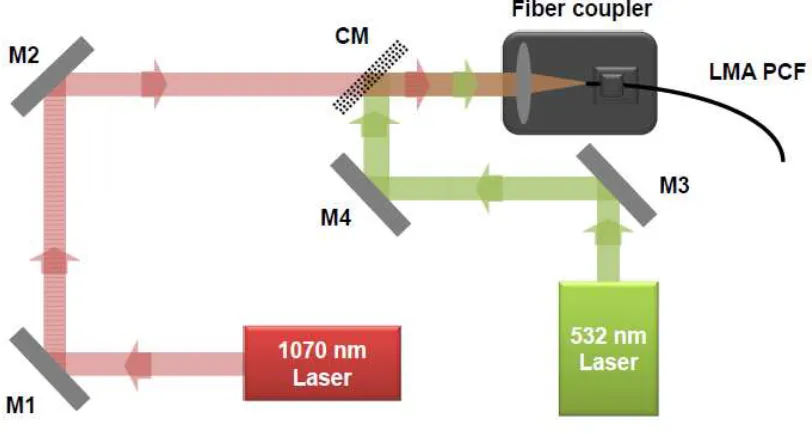
Large Mode Area Photonic Crystal Fiber (LMA PCF) [30] for the beam delivery into the microfluidic channel. The mode profile of the output beam from LMA PCF satisfies the properties required for efficient spatial separation through optical chromatography, details of which are discussed in the latter part of this article. The endlessly single mode property of the LMA PCF is exploited to launch multiple wavelengths, namely one beam at 1070nm to achieve spatial separation, and another at 532nm to achieve in situ
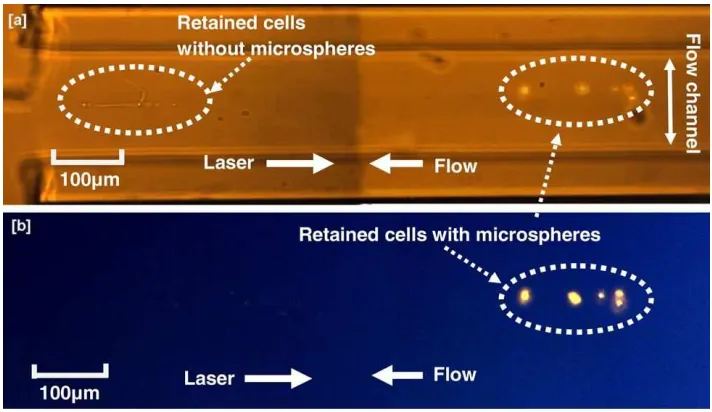
fluorescence excitation. This study also address one of the key problems with passive optical sorting, namely the fact that biological cells of similar size are difficult to distinguish [31]. The difference between healthy and diseased cells of the same species is typically much smaller compared to the natural variation in size and refractive index within a given cell population. This study has addressed this issue by tagging the target cell population with internalized microspheres through phagocytocis. While demonstrating the concept here with populations that have been allowed to internalize the microspheres verses others that have not, one can envisage that this technique could be used to discriminate between healthy and diseased cells by selective uptake of spheres with a specific antibody, thus greatly amplifying their difference in optical properties and making them easily distinguishable [32].
3.2
Theory of optical chromatography
The theoretical value of retention distance can be calculated by equating the fluid drag force and optical radiation force. In 1997 a theoretical model for optical chromatography of dielectric particles was reported with a ray optics approach for calculating the optical radiation force [24], which is briefly described in this section.
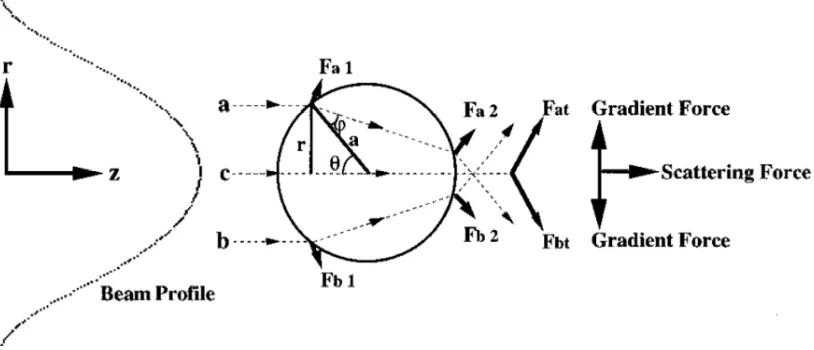
The model assumes a dielectric sphere irradiated by a TEM00 mode laser beam.
Since the laser is lightly focused, the wavefront of the irradiated beam can be assumed to be equivalent to a plane wavefront for particle diameter less than the beam waist of the beam (a<ω).
Considering only the scattering force, the conversion efficiency from an optical radiation to the pressure applied on the particle can be calculated in terms of Fresnel reflection and transmission coefficients as:
2
2
1 ( {cos(2 2 ) cos(2 )})
( ) [1 cos(2 ) ]
2 (1 2 cos(2 ))
T R
Q R
R R
θ ϕ θ θ θ
θ
− +
= + −
+ + (3.1)
Where, T and R are Fresnel transmission and reflection coefficients. The angles
[image:44.595.113.520.458.633.2]specified in the equation are shown in [24].
2 2
2 2
1 sin (
)
tan (
)
2 sin (
)
tan (
)
R
θ ϕ
θ ϕ
θ ϕ
θ ϕ
−
−
=
+
+
+
(3.2)2 2 2
1 sin 2( ) sin( )
sin 2( ) sin( )
2
sin (
)
sin (
) cos (
)
T
θ
ϕ
θ
ϕ
θ ϕ
θ ϕ
θ ϕ
=
+
+
+
−
(3.3)If n1 and n2 are the refractive indices of the surrounding medium and particle, the
angles θ and are related by Snell’s law as:
( )
1
sin
sin( )
2n
θ
=
n
ϕ
(3.4)The radiation force as a function of incident angle is given by
( )
( )
n P1F Q
c
θ = θ (3.5)
( )
( )
n dP1dF Q
c
θ = θ (3.6)
Where, dP is the power of the incident beam on a small area of the particle
The intensity of the laser beam varies in transverse direction as:
2 2
2
0 r
I
I e
ω
−
=
(3.7)Where I0 is the intensity at the beam center and ω is the beam waist of the Gaussian
beam.
( )
a sin
r
=
θ
(3.8)Hence
2 2
0 2
2 sin ( ) exp a
I I θ
ω
=
(3.9)
( )
2 22
0 2
2 ( )
2 sin 2 exp a sin
dP πrdr I πa θ I θ dθ
ω
= =
(3.10)
Substituting dP in equation (3.6) and assuming
2 1 a ω <<
, total force due to
2 * 1
2
R
n P a
F Q
c ω
=
(3.11)
Where,
( ) ( )
2 * 0 sin 2Q Q d
π
θ θ θ
=
∫
(3.12)For Gaussian beams,
2 2 2 0 1 c z z
ω =ω +
(3.13)
Where z is the Rayleigh range given by c
2 1 0 c n z πω λ = (3.14)
The force on the particle due to fluid flow can be expressed using Stokes law for a particle moving with a velocity v as:
6
f
F = πηav (3.15)
Where, η is the viscosity of the medium, where the particle is suspended.
The expression for retention distance z can be calculated by equation FR and Ff as:
2 *
1 0 1
2 0
1
3
n
n PQ a
z
vc
πω
λ
πη ω
=
−
(3.16)From the equation it is clear that retention distance depends on the radius of the particle and refractive index of the particle. Larger particles will have larger retention distance also higher refractive index particles will also have a larger retention distance. The retention distance can be adjusted by changing the fluid flow rate or the power of the laser beam.
3.3
History of optical chromatography
flow. A lightly focused counter-propagating free-space laser beam was aligned parallel to this fluid flow. The optical gradient forces trapped the particle along the center of the laser beam and accelerated it against the fluid flow, away from the beam waist due to the radiation pressure. Counter to this, the Stokes fluid drag force decelerated the particle until finding an equilibrium position where the fluid drag force and radiation force balanced. The distance between the equilibrium position and the beam waist was termed the retention distance. The value of the retention distance was found to be dependent upon the size of the particle, and later also the refractive index [34] and hydrodynamic profile (predominantly shape) of the particle [29]. The retention distance is also a function of the laser power and fluid flow rate. It was in this first paper that the technique was termed optical chromatography due to its ability to obtain classical chromatography-like separations of various species of samples.
In a second paper from the same group [24], the analogies between their new technique and the conventional equivalent were extended through the development of a theoretical model, which until recently has underpinned all experimental work in the field. A ray optics approach was applied to the particle-light field interaction for a propagating Gaussian beam, and balanced by the Stokes fluid drag force. From this various parameters were obtainable, as functions of particle size and refractive index, which were directly analogous to those in classical chromatography. The retention distance (as opposed to retention time), selectivity, theoretical plate number, and resolution were calculated as a function of the laser power, flow rate, particle size and refractive index. The technique was compared to other separation techniques, such as field flow fractionation, gas and liquid chromatography, and size exclusion chromatography.