Optimizing the internal electric field distribution of alternating current driven organic
light-emitting devices for a reduced operating voltage
Markus Fröbel, Simone Hofmann, Karl Leo, and Malte C. Gather
Citation: Applied Physics Letters 104, 071105 (2014); doi: 10.1063/1.4865928
View online: http://dx.doi.org/10.1063/1.4865928
View Table of Contents: http://scitation.aip.org/content/aip/journal/apl/104/7?ver=pdfcov Published by the AIP Publishing
Articles you may be interested in
Fundamental properties of light-emitting liquid crystal cells operated under alternating voltage J. Appl. Phys. 114, 053108 (2013); 10.1063/1.4817173
Degradation studies on high-voltage-driven organic light-emitting device using in situ on-operation method with scanning photoelectron microscopy
Appl. Phys. Lett. 93, 133310 (2008); 10.1063/1.2994668
Improving organic light-emitting devices by modifying indium tin oxide anode with an ultrathin tetrahedral amorphous carbon film
J. Appl. Phys. 98, 046107 (2005); 10.1063/1.2032610
Mixed host organic light-emitting devices with low driving voltage and long lifetime Appl. Phys. Lett. 86, 103506 (2005); 10.1063/1.1879093
High-efficiency polymer light-emitting devices using organic salts: A multilayer structure to improve light-emitting electrochemical cells
Optimizing the internal electric field distribution of alternating current
driven organic light-emitting devices for a reduced operating voltage
Markus Frobel,€ 1,a)Simone Hofmann,1Karl Leo,1and Malte C. Gather1,2 1
Institut f€ur Angewandte Photophysik, Technische Universit€at Dresden, George-B€ahr-Strasse 1, 01069 Dresden, Germany
2
School of Physics and Astronomy, University of St Andrews, North Haugh, St Andrews KY16 9SS, United Kingdom
(Received 7 November 2013; accepted 1 February 2014; published online 18 February 2014)
The influence of the thickness of the insulating layer and the intrinsic organic layer on the driving voltage of p-i-n based alternating current driven organic light-emitting devices (AC-OLEDs) is investigated. A three-capacitor model is employed to predict the basic behavior of the devices, and good agreement with the experimental values is found. The proposed charge regeneration mechanism based on Zener tunneling is studied in terms of field strength across the intrinsic organic layers. A remarkable consistency between the measured field strength at the onset point of light emission (3–3.1 MV/cm) and the theoretically predicted breakdown field strength of around 3 MV/cm is obtained. The latter value represents the field required for Zener tunneling in wide band gap organic materials according to Fowler-Nordheim theory. AC-OLEDs with optimized thickness of the insulating and intrinsic layers show a reduction in the driving voltage required to reach a luminance of 1000 cd/m2 of up to 23% (8.9 V) and a corresponding 20% increase in luminous efficacy.VC 2014 AIP Publishing LLC. [http://dx.doi.org/10.1063/1.4865928]
Inorganic alternating current electroluminescent devices (AC-ELs) were first reported in 1936 and have been under investigation for the past seven decades.1The key-advantage of these devices is their ruggedness and long-term reliability which is why they can often be found in industrial and medi-cal equipment as well as in applications in the military sec-tor.2AC-ELs are based on a phosphor layer which is doped with luminescent impurities. The presence of a high field leads to impact excitation of these impurities and the subse-quent decay to the ground state results in light emission.3 However, due to the low photoluminescent quantum yield of inorganic phosphors and due to the lack of full color capability—a problem which has only quite recently been solved—AC-ELs are nowadays mostly found in niche appli-cations where their unique properties are required.
In contrast to inorganic phosphors, organic materials offer a number of advantages, in particular a higher effi-ciency, easier processibility, and a wide selection of emitter materials spanning the entire visible spectrum. Several efforts towards AC organic light-emitting devices (AC-OLEDs) have been made in the recent past, and even white-emitting AC-OLEDs have been successfully demonstrated.4–8 However, the majority of these devices rely on charge injec-tion from one or even both electrodes and show poor per-formance when operated in a full insulating, capacitively coupled mode, i.e., in a configuration where two insulators prevent charge injection from both electrodes. For this partic-ular configuration, the most promising approach in terms of brightness and efficiency is a p-i-n based architecture in which a single emissive unit is surrounded by doped hole and electron transport layers (HTL/ETL) and by a pair of insulat-ing layers; the whole stack is then sandwiched between two electrodes.9–12The insulating layers prevent current injection
from the electrodes when a DC voltage is applied to the de-vice. Application of a forward voltage pulse, however, drives free electrons and holes from the doped transport layers into the emissive unit, where they can radiatively recombine. The emission from the device stops once the free charge carriers available within the device are depleted. The device can be restored by applying a reverse voltage that replenishes the charge reservoir in each transport layer through a Zener tun-neling process.12,13 The tunneling mechanism strongly depends on the electric field across the intrinsic layers within the p-i-n based AC-OLED. This field can be tuned by the ca-pacitance of the insulating layers as well as by the thickness of the intrinsic organic layers.
In this Letter, we study the influence of the thickness of the insulator layer and the intrinsic organic layer on the driv-ing voltage of p-i-n based AC-OLEDs. We further compare our findings with theoretical predictions which are based on the sample geometry, material constants, and the assumption of Zener tunneling as the most probable mechanism for charge regeneration. We observe a reduction in driving volt-age with increasing insulator capacitance as well as with decreasing thickness of the intrinsic organic layer. Our find-ings are in good agreement with theoretically calculated val-ues based on a three-capacitor device model. The obtained onset field strengths for light emission are close to the pre-dicted breakdown field strength for Zener tunneling in the wide gap organic materials used in this study.
A series of devices with the p-i-n device architecture illustrated in Fig.1was fabricated. All layers were deposited in a UHV chamber at a base pressure of about 108 mbar onto glass substrates coated with structured tin-doped indium oxide (ITO) which acts as transparent bottom electrode. Doping was realized by co-evaporation of the matrix mate-rial and the dopant. The HfO2insulating layers were
depos-ited by radio frequency (RF) magnetron sputtering in a high a)
Electronic mail: [email protected]
purity argon atmosphere without any reactive gas at a pres-sure of 5103mbar. A rate of 2 A˚ /s was achieved for an RF power of 100 W. For the second insulating layer located on top of the organic material, the power was reduced to 60%–70% of its initial value to prevent sputter-induced dam-age of the underlying organic material. HfO2was chosen as
insulating material because of its high dielectric constant and therefore strong polarizability, as well as the high band-gap of 5.8 eV which provides sufficiently high injection barriers for both holes and electrons.15
For the p-type and n-type transport layers, we used N,N,N0,N0-tetrakis(4-methoxyphenyl)-benzidine (MeO-TPD) doped with 6 wt. % 2,20-(perfluoronaphthalene-2,6-diylidene) dimalononitrile (F6-TCNNQ) and 4,7-diphenyl-1,10-phenanthroline (BPhen) doped with cesium (Cs), respec-tively. An electron and a hole blocking layer (EBL/HBL) were used to confine the charge carriers and excitons inside the emission layer (EML). The HBL was realized using a layer of BPhen, whereas 2,20,7,70 -tetrakis-(N,N-diphenyla-mino)-9,90-spirobifluorene (Spiro-TAD) was used for the EBL. The EML consists of N,N0-di(naphthalen-1-yl)-N-N0 -diphenyl-benzidine (a-NPD) doped with 10 wt. % of the highly efficient phosphorescent red emitter Iridium(III)bis (2-methyldibenzo-[f,h]chinoxalin)(acetylacetonat) (Ir(MDQ)2
(acac)). A 100 nm thick layer of aluminum was used as highly reflective top electrode. The active area A of the device is determined by the overlap of bottom and top electrode, which was 5.96 mm2. Prior to device investigation, the samples were encapsulated in a nitrogen glovebox.
The thickness of the intrinsic EBL and HBL is denoted withx, and the thickness of the EML is denoted withy. We tested four devices with x/y¼10 nm/20 nm, 10 nm/15 nm, 10 nm/10 nm, and 7.5 nm/10 nm, respectively. The thickness of the HfO2insulating layer was 120 nm for these four devices
(Fig.1(a)). In another series of devices, the thickness of the HfO2layer was varied using the intrinsic layer configuration
withx/y¼7.5 nm/10 nm. Here, we varied the oxide thickness fromz¼120 nm to 180 nm in 20 nm steps (Fig.1(b)).
Optical simulations based on a radiative dipole model were used to model the light-extraction efficiency and to ensure that the outcoupling efficiency is comparable in all
devices.14This was achieved by adjusting the HTL and ETL thickness (dHTL, dETL) such that the recombination zone was
located in the maximum of the optical field in all devices. dHTL was varied between 74 nm and 88 nm and dETLranged
from 50 nm to 108 nm. Due to the use of doped HTLs and ETLs, the variation in transport layer thickness was not expected to lead to significant changes in electrical device characteristics.
The electrical driving of the samples, the measurement setup, and the correct determination of the luminous efficacy for this kind of devices have been described in previous pub-lications.8,12 All measurements were performed at a fixed frequency of 5 kHz. Voltages are given as RMS (root-mean-square) values if not stated otherwise.
In previous studies on p-i-n AC-OLEDs, we assumed Zener tunneling of electrons from the HOMO of the p-type layer to the LUMO of the n-type layer to be responsible for refilling the depleted transport layers and to provide charge carriers for light emission. In low gap organic tunnel diodes, Zener breakdown occurs at field strengths of 1. 1.5 MV/cm.13,16In the wide gap materials used in this study, a breakdown field strength of around 3 MV/cm for Zener tun-neling is predicted, assuming a triangular tuntun-neling barrier where the relation between electric breakdown field Fband
energy gapEgis given byFbE 3=2
g (Fowler-Nordheim).17 The AC-OLED can be modeled electrically as a series of three capacitors with capacitors 1 and 3 representing the insu-lating layers and capacitor 2 being the intrinsic organic mate-rial, that is, EBL, EML, and HBL. For capacitors connected in series, the transferred chargeQis a constant given by
Q¼C1DV1 ¼C2DV2¼:::¼const:; (1)
where Cis the capacitance andDV the voltage drop across the corresponding capacitor. The electrodes as well as HTL and ETL of our devices are highly conductive; thus, the volt-age drop across these layers can be neglected. The driving voltageVdis therefore the sum of the drop in voltage across
the three capacitors in the device
[image:3.612.50.421.566.774.2]Vd ¼2DVoxþDVorg: (2)
FIG. 1. Schematic illustration of the stack architecture of the investigated devices for (a) the thickness variation of the intrinsic organic layers and (b) the variation of the oxide thickness, respectively. For all devices, the recombination zone is shifted to the optical field maximum by adjusting the HTL and ETL thickness (dHTL,
dETL).
Using Eqs. (1) and (2),DVox andDVorg can be calcu-lated. Division by the respective layer thickness yields the electric field across the insulating oxide layers Foxand the
intrinsic organic layersForgaccording to
Forg¼
Vd
dorg 2 Corg
Cox þ1
; (3)
Fox¼
Vd
dox Cox Corg
þ2
¼org
ox
Forg: (4)
The capacitance of the oxide layers as well as the intrin-sic organic layers can be calculated from the active area A and the corresponding dielectric constant of each material which isox¼23 in case of HfO2andorg2:8 in case of the organic material. Using these values and Eq. (3), the driving voltage required to reach a certain field strength across the intrinsic organic layers can be estimated.
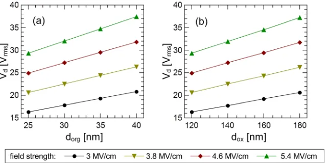
Figure 2(a) shows the driving voltage Vd required for
four different field strengths as a function of the different intrinsic organic layer thicknesses used in this study. These calculations show that reducing the intrinsic organic layer thickness by 5 nm results in reduction in driving voltage of around 1.5 V and 2.7 V for field strengths of 3.0 MV/cm and 5.4 MV/cm, respectively. Similar results are obtained when varying the thickness of the insulating oxide layer and com-parable reductions in driving voltage are expected (Fig.2(b)). The field strength in the oxide layers and the intrinsic or-ganic layers are linearly correlated through the ratio of the dielectric constants of these layers (Eq.(4)). Thus, even for very highForgvalues of 5.4 MV/cm, the field across
insulat-ing HfO2 layers is only 0.66 MV/cm and therefore lower
than the breakdown field strength of HfO2which is in the
range of 1–2 MV/cm. Charge carrier injection can therefore be ruled out as origin of exciton formation in our devices as we have already shown in previous publications.9,10,12
The experimental results of our first series of devices with different thickness of the intrinsic organic layer (Fig.1(a)) are summarized in Fig.3. While the general shape of the luminance-voltage curves remains identical for all thicknesses, the voltage required to achieve a certain bright-ness can be considerably reduced when reducing the thick-ness of the intrinsic organic layers (Fig. 3(a)). A 5 nm
reduction in intrinsic organic layer thickness leads to a decrease in driving voltage by approximately 1.5–2 V which is in good agreement with the values in Fig. 2(a). We can identify two distinct regions in each luminance curve. The first region (approximately 1–10 cd/m2), for which the lumi-nance is only slowly increasing with voltage, is mainly gov-erned by small residual leakage currents and not tunneling. This parasitic leakage current regime is also present in low-gap organic tunnel diodes.13,16 The second region (>10 cd/m2), for which the slope of the luminance curve is greatly increased, can be ascribed to the Zener tunneling re-gime where tunneling currents are the major contribution to charge regeneration. The transition from the first to the sec-ond is defined as the onset of tunneling. Interestingly, the field strength at the onset is close to 3.05 MV/cm for all four samples (Fig. 3(b)). This value is in good agreement with theory according to which the transition to the tunneling re-gime is supposed to occur at around 3 MV/cm.
When varying the thickness of the HfO2 oxide layer
(Fig.4), we observe an almost identical behavior as for the variation of the intrinsic organic layers (Fig.3). Most impor-tantly, the onset field strengths are again very similar for devices with different oxide layer thickness and again agree with the expected value of3 MV/cm (Fig.4(b)).
Additionally, Figs. 3(b) and 4(b) also show the esti-mated field strength across the intrinsic organic layers required for a device luminance of 100 cd/m2 and 1000 cd/m2. As for the onset of luminance, the field strength is nearly identical for all intrinsic and insulating layer thick-nesses investigated here. The field required for a luminance of 100 cd/m2and 1000 cd/m2is 3.8–3.9 MV/cm and 5.5–5.6 MV/cm, respectively.
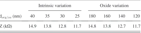
TableIsummarizes the expected impedance of all sam-ples in this study. These values were calculated for a fre-quency of 5 kHz using only the sample geometry and the dielectric constants of the involved materials. Similar values were obtained for the variation in intrinsic layer thickness and for the variation in oxide thickness.
[image:4.612.94.297.111.196.2]The experimentally obtained impedance values for the variation of the intrinsic organic layers and the insulating layers are shown in Figs.3(c)and4(c), respectively. The low voltage impedance is consistent with the theoretically pre-dicted value for the respective layer thicknesses for all sam-ples in this study. The tunneling onset can be clearly distinguished in Figs. 3(c) and 4(c) as a sudden drop in
FIG. 2. Calculated driving voltageVd
[image:4.612.52.376.610.770.2]impedance at a voltage which coincides with the onset volt-age derived from the luminance curves. At this point, the intrinsic organic layers lose their capacitive nature due to injection into this formerly depleted region. The overall de-vice capacitance, which is now only determined by both insulating layers, increases, and the measured impedance is reduced accordingly.
Figures3(d) and 4(d)show the luminous efficacy as a function of the luminance. As a result of the reduced driving voltage, the luminous efficacy is increased by up to 20% for both types of variation.
In summary, the influence of the insulator thickness and the intrinsic organic layer thickness on the driving voltage of p-i-n based AC-OLEDs was investigated. A three-capacitor
FIG. 4. Electrical characteristics of a series of AC-OLEDs with different thicknesses of the insulating HfO2
oxide layers and a constant intrinsic layer thickness of 25 nm. (a) Voltage-luminance characteristics and (b) field strength derived from these character-istics to reach the light emission onset, 100 cd/m2and 1000 cd/m2, shown as a
function of the insulator thickness. (c) Voltage-impedance characteristics and (d) luminous efficacy for the different devices.
FIG. 3. Electrical characteristics of a series of AC-OLEDs with different thicknesses of the intrinsic organic layers, that is, EBL, EML, and HBL, and constant thicknesses of the HfO2
oxide layers of 120 nm. (a) Voltage-luminance characteristics and (b) field strength derived from these character-istics to reach the onset of light emis-sion, as well as luminance levels of 100 cd/m2and 1000 cd/m2, shown as a function of the intrinsic organic layer thickness. (c) Voltage-impedance char-acteristics and (d) luminous efficacy for the studied devices.
model was employed for basic device behavior predictions and good agreement with the experimental values was obtained. For all samples, the measured device impedance was close to the calculated value which indicates that the thickness of all layers was controlled precisely and that no inductive or parasitic, Ohmic loss channels are present. Furthermore, we showed that a significant increase in light emission occurs at field strengths of 3–3.1 MV/cm across the intrinsic organic layers, in agreement with Fowler-Nordheim theory predicting, a minimum field strength of 3 MV/cm required for Zener tunneling in wide band gap organic mate-rials. In terms of device improvement, we were able to reduce the driving voltage by up to 23% which results in a luminous efficacy enhancement of 20%. Reducing the insu-lating layer thickness below 120 nm can lead to further improvements in driving voltage. However, thin oxide layers are prone to increased leakage currents which result in low-ering the luminous efficacy of the device. A further reduction of the intrinsic organic layers is also limited, as EML and
blocking layers require a certain minimum thickness for effi-cient exciton generation and exciton blocking.
This work was funded with financial means of the European Social Fund and the Free State of Saxony through the OrthoPhoto project.
1
G. Destriau, J. Chim. Phys.33, 587 (1936).
2
P. F. Smet, I. Moreels, Z. Hens, and D. Poelman,Materials3, 2834 (2010).
3D. C. Krupka,J. Appl. Phys.43, 476 (1972). 4
Y. Z. Wang, D. D. Gebler, L. B. Lin, J. W. Blatchford, S. W. Jessen, H. L. Wang, and A. J. Epstein,Appl. Phys. Lett.68, 894 (1996).
5
T. Tsutsui, S.-B. Lee, and K. Fujita,Appl. Phys. Lett.85, 2382 (2004).
6J. Sung, Y. S. Choi, S. J. Kang, S. H. Cho, T.-W. Lee, and C. Park,Nano Lett.11, 966 (2011).
7
Y. Chen, Y. Xia, G. M. Smith, Y. Gu, C. Yang, and D. L. Carroll,Appl. Phys. Lett.102, 013307 (2013).
8M. Fr€obel, A. Perumal, T. Schwab, C. Fuchs, K. Leo, and M. C. Gather, Phys. Status Solidi A210, 2439 (2013).
9
A. Perumal, M. Fr€obel, S. Gorantla, T. Gemming, B. L€ussem, J. Eckert, and K. Leo,Adv. Funct. Mater.22, 210 (2012).
10A. Perumal, B. L€ussem, and K. Leo,Appl. Phys. Lett.100, 103307 (2012). 11A. Perumal, B. L€ussem, and K. Leo,Org. Electron.
13, 1589 (2012).
12
M. Fr€obel, A. Perumal, T. Schwab, M. C. Gather, B. L€ussem, and K. Leo,
Org. Electron.14, 809 (2013).
13H. Kleemann, R. Gutierrez, F. Lindner, S. Avdoshenko, P. D. Manrique,
B. L€ussem, G. Cuniberti, and K. Leo,Nano Lett.10, 4929 (2010).
14
M. Furno, R. Meerheim, S. Hofmann, B. L€ussem, and K. Leo,Phys. Rev. B
85, 115205 (2012).
15J. Robertson,Eur. Phys. J. Appl. Phys.28, 265 (2004).
16H. Kleemann, K. Leo, B. L€ussem, R. Gutierrez, S. Avdoshenko, and G.
Cuniberti,Org. Electron.14, 193 (2013).
17
[image:6.612.52.298.69.127.2]R. H. Fowler and L. Nordheim,Proc. R. Soc. London, Ser. A119, 173 (1928). TABLE I. Calculated device impedance Z for a frequency of 5 kHz.
Intrinsic variation Oxide variation
dorg=ox(nm) 40 35 30 25 180 160 140 120