Design Optimization of Quasi-Active Gate
Control for Series Connected Power Devices
Nithiphat Teerakawanich
†, and C Mark Johnson
Abstract
This paper presents a new gate drive circuit for driving a series string of IGBTs. The proposed quasi active gate
control (QAGC) circuit is simple to implement as it composes of only a few passive components in addition to a
standard gate driver. No separate isolation power supply is required for the upper devices in the stack. The proposed
QAGC circuit provides an effective way to drive the power devices and control static and dynamic voltage sharing to
the devices at the same time. The theoretical switching operation and the oscillation stability analysis allow criteria
for component selection to be established. Limitations of the QAGC circuit is also identified. The modification of
the circuit to support more power devices in the series stack is discussed with the aid of the simulation results. The
switching operation of the circuit is validated from the experimental results using 2 IGBTs connected in series. The
circuit shows a satisfied switching operation with well-controlled dynamic and static voltage sharing and comparable
gate voltage between the coupled devices.
Index Terms
Active gate control, power devices, series connection, gate driver, voltage balancing circuit.
†Corresponding author (e-mail: [email protected])
The authors are with PEMC group, Department of Electrical and Electronics Engineering, University of Nottingham, Nottingham, NG7 2RD,
Design Optimization of Quasi-Active Gate
Control for Series Connected Power Devices
I. INTRODUCTION
Power electronic systems are accepted as the key technology to convert and control electrical power flow from one form to another efficiently. A scale of applications could range from a fraction of watt found in consumer products to a giga-watt scale found in utility applications. In some high power applications, there may be case where a power switch used in the converter is in a form of multiple power semiconductor devices combined in series or parallel configuration in order to create a higher voltage or higher current switch respectively. For example, the 150-kV VSC-based HVDC transmission system presented in [1] utilises more than 20 IGBTs in one stack of the switches and connect up to 10 stacks in series to achieve the rated voltage. A high voltage Marx generator in [2] is another example where twelve IGBTs are connected in series to form a single switch with 10 kV and 300 A ratings. In some cases, using low-voltage semiconductor devices as a building block to achieve higher voltage switches is preferred over using a single high voltage device for the better switching performance like the scalable power semiconductor switch (SPSS) developed in [3].
However, the process to assure that no particular device exposes to a higher voltage than the other is difficult in practice as even a slight deviation of the gate signal delay or switching speeds can result in unbalanced voltage distribution across the devices in series connection. Therefore, it is one of the key challenges for the designer to provide voltage balancing methods to the series string to prevent the power devices from a subsequent failure due to an overvoltage and excessive losses.
The static voltage balancing under blocking condition is usually achieved by placing a voltage-divider resistor in parallel with the power device to compensate for device leakage current. However, it is more difficult to balance the voltage during the dynamic period. There are many methods that have been introduced to ensure an equal dynamic voltage sharing. Use of a passive snubber network whether RC or RCD circuits on the power-side of power devices to slow down the switching seems to be the most popular and simplest method to implement as suggested by [4]. However, this method delivers additional losses in bulky passive devices. Therefore, another approach utilizing gate driver control appears to be more attractive due to low power components used in its circuit.
RCD snubber and active clamping has been demonstrated in [10] to optimize the total losses. More complicated active control methods may employ feedback control loops [5], [11], [12]. An active voltage control method (AVC) includes feedback control loops to control both dV /dt and overvoltage level of the power devices so that every device follows the same switching trajectory defined from the voltage reference profile [11]. Similarly, the active voltage balancing circuit in [5] involves device voltage control loops to adjust the delay time of each gate signal according to the overvoltage level of the device. Nevertheless, the major drawback of theses methods is complexity and additional cost of control circuits to the gate driver.
A simple technique, quasi active gate control (QAGC), has been proposed in [13]. The proposed method is for series operation of voltage driven power devices. It provides dynamic and static voltage sharing by using a simple RC balancing network and a single gate driver. This paper aims to elaborate on the procedure of parameter design and optimization of the proposed QAGC circuit by taking into account switching transient and stability criteria. In addition, a modified QAGC circuit is proposed in order to support the extension of the QAGC series string. The operation of the QAGC circuit is discussed first in section II. Then, the circuit design criteria are established in section III. A modified circuit is presented in section IV. The circuit is finally validated by the experimental results which are given and discussed in section V.
II. CONCEPT OFQAGC CIRCUIT
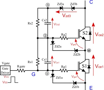
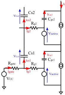
In Fig. 1, the proposed QAGC circuit drives two IGBTs connected in series to perform as a single switch. Actually, the QAGC circuit is equally good for driving the series string of other voltage-driven devices such as power MOSFETs and JFETs as shown in [13]. The circuit composes of only a standard gate driver and passive devices so it is very simple to implement. The component count is obviously an advantage over the other active control methods considering that those methods require a separate gate drive unit for every power device. The RC balancing network induces the switching operation of the upper switch and acts as adV /dtsnubber of the power devices at the same time. The zener diodes Zd1 andZd2 are included to protect the gate from overvoltages and
provide paths for device leakage currents whileZd3 allows a level shift to prevent static conduction from the gate
circuit to the drain circuit.
The proposed QAGC circuit may be put in the same category as the circuits proposed by [14] and [15] in the sense that all circuits switch the series-connected power devices on and off by using the dV /dt action of the lower device to induce the switching of the device above it. Having said that, the QAGC circuit still differs from those mentioned circuits in many ways. The main differences are that initial turn off delay which normally causes sequential switching in these configurations can be diminished by an interdependent mechanism between RC network (Rs and Cs) and the power devices. The circuit also provides more control over dV /dt and static
Rs2
Rs1 Cs2
Cs1
Rgate
Zd1a
Zd1b Zd2a
Zd2b Zd3a Zd3b
S1 S2
C
E
G 1
2
M 3
Vgate Gate Driver
Vge1 Vge2
Vce2
Vce1
Rg2
Rg1 VCs1 VCs2
VEE VCC
[image:4.612.216.397.72.229.2]Vzd3
Fig. 1. QAGC circuit for two devices connected in series
Vgate Vge1
Vge2
Vce1
Vce2
Idevice
t0 t1 t2 t3
VEE
VCC
Vth
Vactive
Fig. 2. Waveforms during the turn-on sequence
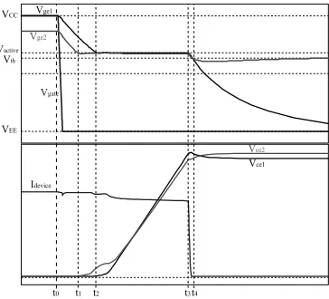
A. Turn-On Operation
The operation of the circuit during turn-on process can be described by a sketch of simulated waveforms in Fig. 2 and by the circuit voltage relationships in (1) and (2).
V1E+VCs1=V2M +Vce1 (1)
V2M+VCs2=VZd3+Vce2 (2)
Initially,Vce1,Vce2, andVge2stay at their steady state voltages which are determined by the voltage divider network
(Rs1,Rs2) and balance of device leakage currents. Both devices are assumed to have identical leakage current for
simplicity. The voltageVge2 is considered to stay just below the threshold voltage (Vth) ( this will be shown later
in the section).
[image:4.612.215.400.275.453.2]Vactive ICgc1
Ig1 Igate
Ics1
VCC
Rgate Rg1 Cgc1 Cs1
VCs1
Vactive IL
ICgc2
Ig2 Ics2
Rg2 Cgc2 Cs2
[image:5.612.250.359.71.229.2]VCs2
Fig. 3. Gate current flow during turn-ondV /dt
toVCC shifting up the voltage potentialV1E by nearly the same amount. According to voltage relationship in (1)
and (2), voltage balancing mechanism forces anVce1 to increase which is countered by a drop inVce2 to maintain
the level of DC bus voltage (Vdc) as suggested in the waveforms duringt0tot1. During this period,Vge1 continues
to charge up and yet to reach Vth whileVge2 remains just above the threshold voltage.
WhenVge1 reachesVthatt1, the impedance of S1 starts to drop thus allowingVce1 to fall. This action is again
countered by an increase inV2M ; therefore,Vge2can be raised up aboveVthas well asVge1automatically. During t1 tot2 , the load current starts to commutate to the devices following the device transfer characteristics.
At the timet2when current commutation is completed, both devices are entering the active region;Vge1andVge2
reach the plateau voltage which is determined by device transconductance (gm) and load current (IL). The voltages
Vce1 andVce2 start to fall almost simultaneously so that no voltage overshoot occurs. It is during t2 tot3 that the
capacitorsCs1andCs2play an important role. The gate charge required for the upper device is extracted from the
discharging currents ofCs1 and Cs2. The voltage transition speed dV /dtof the power devices are controlled by
these capacitors and the gate resistors as expressed in (3) which is derived from the current flow in Fig. 3 under the assumption thatdVce1/dtis approximately equal todVCs1/dt.
dVce1
dt ,on=
Vth+gImL −VCC
Rgate(Cs1+Cgc1) +Rg1Cgc1
(3) Turn-on transient is finished at the end of the active region. Aftert3,Vge1 andVge2 continue rising further and
eventually bring the devices into the saturation region subject to their available gate charge. There is no concern overVge1as the gate charge is supplied directly from the power supply. However, the required gate charge for S2 to
bringVge2 out of the Miller plateau is limited. Though the gate driver supplies the charging current to S2 through Rs1 during this period, the time constant to increaseVge2 to its full gate voltage is too long due to a big value of Rs1 so it is insufficient in a normal PWM operation. Therefore, it is better to provide the required gate charge just
right after t3 by other means. The further discussion on improving the gate turn on voltage will be given in the
Vgate Vge1
Vge2
Vce1 Vce2
Idevice
VCC
Vth
Vactive
t0 t1 t2 t3t4
[image:6.612.216.398.70.235.2]VEE
Fig. 4. Waveforms during the turn-off sequence
device on-state voltages.
B. Turn-Off Operation
The process of turn-off operation can be described with the help of the diagram in Fig. 4. The relation ships in (1) and (2) are still applicable.
Initially, both devices are in the saturation region. The gate voltageVge1is equal to the gate drive power supply VCC while Vge2 is lower. Turn-off sequence starts att0 when Vgate changes fromVCC toVEE causing a sudden
drop in both V1E and V2M. The gate capacitances of both IGBTs are discharged simultaneously. At the timet1, Vge2 falls to the Miller plateau before Vge1 due to a lower gate voltage so thatVce2 starts rising first while Vce1
remains constant. The QAGC circuit takes action by increasingV2M to balance a rise inVce2. Discharging current
of the upper device is then restricted causingVce2 to slows down as can be noticed in the waveforms.
After some delay, the voltageVge1 reach the Miller plateaut2 and both devices are in the active region.Vce1and Vce2 start to ramp up together. From t2 tot3, the balancing capacitorsCs1 andCs2 take full dynamic control of
the series string. The voltage slopedV /dtcan be determined from the charging rate ofCs1 andCs2 as expressed
in (4).
dVce1
dt ,off=
Vth+gImL −VEE
Rgate(Cs1+Cgc1) +Rg1Cgc1
(4) At the end of thedV /dt period (t3), the whole series string take up the bus voltage VDC. Both devices share
reasonably equal voltage. The load current can now be transferred from the devices to the free-wheeling diodes. The current falls sharply and reaches zero current at t4 while Vge1 andVge2 drop to the threshold voltages. The
load current is completely commutated to the free-wheeling diode and turn-off transient is considered completed. Aftert4,Vge1continues to drop further to the gate turn-off voltageVEE whileVge2stays nearly constant below its
threshold voltage due to slow gate discharging through the high value resistanceRs1. For a normal PWM operation
Vthduring turn off period. Nevertheless, if we allow enough time, the voltageVge2 will fall to the negative value
clamped byZd2. The voltagesVce1 andVce2 also move to their steady state values. If the device leakage currents
are balanced, thenVce1 andVce2 will be determined from the following relationship which is derived from (1) and
(2).
Vce1−Vce2= (VCs1−VCs2)−VZd3+V1E−2V2M (5)
In many cases,V2M will stay just belowVth after dV /dtand the mismatched voltage can be estimated by (6)
given that the typical gate voltage swing is±15V.
Vce1−Vce2= (VCs1−VCs2)−30−2Vth (6)
It is clear that using the QAGC circuit to drive the series string gives rise to a controlled voltage sharing between the devices during the whole switching stages. The voltages across the power devices are contained within the envelope placed by the voltage divider. The following gives more details of the QAGC operation when the devices have difference leakage current characteristics.
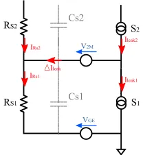
C. Effect of Leakage Current on Voltage Sharing
Practically, leakage currents of individual devices are always unmatched due to manufacturing process. This devi-ation contributes to unbalanced voltage sharing between the devices and the QAGC circuit handles this unbalanced condition in the following ways.
VGE
IRs1
RS2
Cs1
V2M
Ileak2
IRs2
Cs2
RS1
Ileak1
DIleak
S1
[image:7.612.254.358.419.532.2]S2
Fig. 5. Simplified QAGC circuit during turn-off steady state
Fig. 5 shows a simplified circuit during turn-off steady state. The upper device has a higher leakage current than the lower one. The circuit will try to balance the leakage current by lower Vce2 and raise Vce1 until they reach
the limit set by VCs2 and VCs1 respectively. Then, the unbalanced leakage current flows through Zd3 to the RC
the zener diode at the same level asV1E. In this condition, (5) becomes
Vce1−Vce2=VCs1−VCs2
= VDC
(Rs1+Rs2)
(Rs1−Rs2)
+2∆Ileak
Rs1Rs2
(Rs1+Rs2)
(7) where ∆Ileak is the difference between S2 leakage current and S1 leakage current. We can see that unmatched
leakage currents contribute to a higher degree of unbalanced voltage sharing.
However, if the leakage current of S1 is higher, the QAGC circuit would response differently. It will lowerVce1
which allows Vge2 to increase slightly just to allow more leakage current to flow through S2; hence, balancing
the leakage current for both IGBTs. In this circumstance, ∆Ileak is zero and it has no effect on the voltage
sharing. Therefore, it is preferred to operate the QAGC circuit in this condition to ensure that the voltage balancing mechanism is still effective as intended. The next section provides the circuit design criteria to achieve a successful switching operation as discussed in this section.
III. DESIGNCONSIDERATIONS
A. Circuit Parameter Calculations
Firstly, it is recommended to add a shunt resistor to the lowermost power device to ensure that it has the highest leakage current so that the upper device can react to balance the leakage current as mentioned earlier. Its value should be selected such that its current is at least equal to the maximum specified leakage current of the devices.
Then, there are four parameters of the QAGC circuit (Rgate, Rg, Cs and Rs) whose values must be chosen
properly to ensure that the top device can be turned on properly and the DC bus voltage distributes between the coupled devices evenly during turn off. A good starting point is to establish the steady state voltage sharing of the power devices. From (6), we obtain the following relationship that yields an equal voltage sharing in steady state.
VCs1−VCs2= 30 + 2Vth (8)
As a result, we can select the values of static balancing resistorsRs1andRs2to form a voltage divider that satisfies
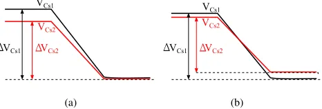
(8). It is noted that a voltage difference between the balancing capacitors provides twofold benefits: firstly, it forces an equal static voltage sharing of the power devices and, secondly, it assists the switching-on operation of the upper device. Current flowing in the resistors should not exceed 5 times the device leakage current to limit resistive loss. Considering the fact that most active control techniques still requires a resistor in parallel with the power device for static voltage sharing, resistive loss associated with the QAGC circuit is just comparable to the other methods. The capacitor values can be calculated based on the turn-on gate charge criteria. The following equation shows the required gate charge during the active region (Qg,active) of the upper device.
If we assume that at the end of the active region VCs1 andVCs2 are equal to Vce,sat of the power devices, then
it is reasonable to approximate∆VCs1 and∆VCs2 from the static voltages as shown in Fig. 6(a). Given thatCs1
andCs2 are equal, then the minimum value forCs1 andCs2 for a successful turn-on operation can be calculated
from the following.
Cs,min=
Qg,active
∆VCs
(10) where∆VCs equals to VCs1−VCs2. It is important to allow enough ∆VCs at the beginning otherwise VCs2 will
end up at high voltage level which is much higher than the device saturation voltage (see Fig. 6(b)).
If the value obtained from (10) is too high, the overall energy consumed from the gate driver will be inefficiently utilised as most of the energy is used for charging the balancing capacitors while only a fraction is used for charging the gate capacitance. For example, if∆VCsis fixed to0.1VCs1, total charge requirement from the main gate driver
(QGDU,total) is:
QGDU,total=Qg+Cs1VCs1.
= 11Qg. (11)
When compare with the total gate charge required for 2 power devices2Qg, the QAGC gate driver has to supply
5.5 times more charge than the standard circuit. Therefore, we come up with another possible scheme to allow a smaller value of Cs to be used; hence, more efficient charge utilization. From (9), if we match dVCs1/dtand dVCs2/dt, the relationship becomes the following:
Cs1−Cs2=
Qg,active
VCs2
. (12)
Then, we can choose any values of Cs1 as long as we keep the difference as in (12). The consequent advantage
of this scheme is that extra gate charge is gained from ∆VCs at the end of dV /dt. This scheme is suitable for a
high-power semiconductor device that requires large amount of gate charge.
VCs1 VCs2
D D
VCs1
VCs2
(a)
VCs1 VCs2
D D
VCs1 VCs2
[image:9.612.193.426.505.584.2](b)
Fig. 6. Capacitors voltages during turn on (a) enough voltage difference (b) not enough voltage difference
OnceCs1is established, the values ofRgateandRgcan be selected according to the switching speed requirement
in (3) and (4). The resistors Rgate andRg should be small for a fast switching but Rg should be big enough for
damping local loop oscillations as will be discussed in section III-B.
The other design consideration is a standard gate driver current rating. It should be sufficient to supply the peak current requirement which has to take into account the capacitor charging and discharging current Cs1
dVCs1
Lg1
IGBT1 C
G
E
Lc1
Le1
Cgc1
Cge1
Cce1 Ro
[image:10.612.249.367.72.167.2]Cj,diode
Fig. 7. Small signal model of the IGBT showing the parasitic elements
Fig. 8. Switching-on waveforms of the QAGC circuit at zero current load and Vdc of 500 V [17]
B. Influence of Circuit Parameters on Stability
The capacitances and parasitic inductances present in the circuit, both inside the power devices (Fig. 7) and in the main circuit path, may resonate and cause oscillation during switching transients. The switching waveforms of the QAGC circuit in Fig. 8 show some oscillations in voltage and current waveforms. Current and voltage oscillations are undesirable as they may cause several issues such as overvoltage transient on the gate, radio frequency noise emission, high switching losses, and could even lead to uncontrolled oscillation and destruction of one or more power devices [16].
From the analysis presented in [17], there are three groups of resonant frequencies which can be identified as the followings.
• For the low frequency mode, the balancing capacitors resonate with the busbar parasitics in the current return path. The oscillation cannot be damped effectively because of a low resistance path.
• For the medium frequency modes, the oscillation seems to be within the local loop between the power devices and the balancing circuit. The device internal capacitances (Cge, Cgc, andCce) resonate mainly with the device
[image:10.612.210.403.220.398.2]Fig. 9. Root loci whenRgvaries from 10 ohms to 50 ohms showing the minimum value ofRg required to keep the complex eigenvalues in
the LHS of the s-plane [17]
suppress the oscillations providing their values are big enough. Fig. 9 shows that the unstable eigenvalues of the system occur ifRg is smaller than 18Ω.
• For the high frequency mode, the oscillation involves the parasitic elements on the load side (bus bar inductances
and load parasitic capacitance). IncreasingRgmandRgonly gives a slight damping improvement for this mode.
The QAGC circuit parameters must be designed to satisfy not only the switching operation but also stability criteria. Commutation loop inductances should be minimised in order to reduce the oscillation modes that cannot be damped effectively by the gate resistors of the QAGC circuit.
IV. SCALABILITYISSUES
This section discusses scalability issues of the QAGC circuit. There are two main concerns about the performance of the circuit when apply to an extension number of the power devices in the series string: how to raise and sustain an appropriate level of the upper gate turn-on voltage and how to minimise an unbalanced dynamic sharing voltage. A modification has to be made to the circuit in order to facilitate these concerns. A discussion is given shortly in this section.
A. Gate Voltage Sustainability
Rs2
Rs1
Cs2
Cs1 Rg1 Rg2
Zd1a
Zd1b
Zd2a Zd2b
Zd3a Zd3b
S1 S2 D
S G
Rb1
Cb1 Db1
[image:12.612.236.380.71.220.2]Db2
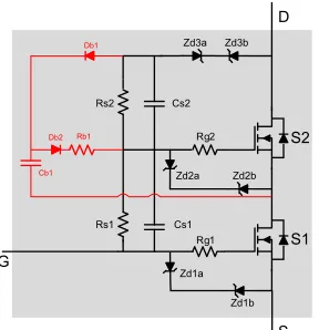
Fig. 10. Modified QAGC circuit
drop in the lower device and in a bootstrap diode; therefore, it may not be suitable for a series stack with a higher number of power devices or a high-power device with a high on-state voltage.
An alternative solution is presented in Fig. 10. The modified QAGC circuit operates in the same manner as the original QAGC except that the boost capacitor Cb1is included to store excessive charge during turn-off transients
and return back to the gate terminal after turn-on transients. The capacitorCb1 is charged to VCs2 during turn off
period. It has to store enough charge to supply to the gate capacitance throughout the turn-on period. Its value is much smaller than Cs as its voltage is very high; therefore, this additional capacitor hardly affects the switching
speed. The value ofCb1 can be calculated from the following: Cb,min>
Qg,f inal
VCs2
(13) where Qg,f inal is the amount of gate charge required to bring the gate voltage to its final value. The resistor
Rb1 serves two functions in this circuit; it limits the speed of dischargingCb1 (or the speed of charging the gate
capacitance) and it is in parallel with Rs2 to set the effective resistance value for a voltage divider. It should be
selected such that the discharging time constant is greater than the longest turn-on period of PWM signals by using the following relationship:
Rb1>
∆ton
Cb1
(14) where∆ton is the longest pulse width of the PWM signal.
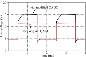
Fig. 11 compares the simulated gate turn-on voltages of the upper device driven by the original and the modified QAGC circuit. The gate voltage with the assistance from the modified circuit rises to 15 V and holds its voltage there even for a long period (1 ms) while the gate voltage from the original circuit increases by 0.5 V only. We can see that a higher gate voltage is achieved with the modified circuit.
0 5 10 15 20
1 2 3 4
time (ms)
Gate
volt
age
(
V
)
with modified QAGC
[image:13.612.221.391.69.183.2]with original QAGC
Fig. 11. Simulated gate voltages of the upper device with and without the modified circuit
B. Extension of a Series String
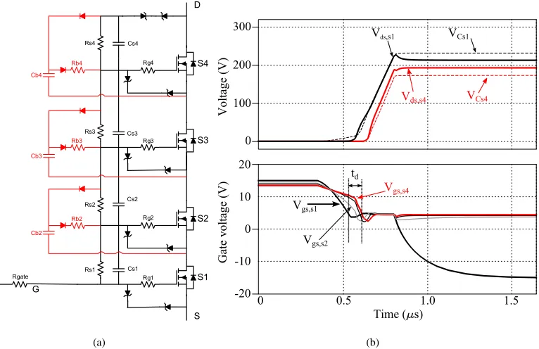
The modified QAGC circuit can be extended for driving an N series-connected power devices as shown in Fig. 12(a) which demonstrates a switch composed of 4 devices in series connection. The circuit arrangement was simulated using SPICE software to validate its operation. MOSFET was chosen over IGBT in this simulation because a MOSFET SPICE model yields a faster, more robust and accurate switching results than the available IGBT model and it has been shown in [13] that MOSFET and IGBT under the QAGC control exhibited the similar switching behaviour. The MOSFET model used in the simulation is IRFP90N20D which requires about 200 nC of gate charge during turn on. The waveforms in Fig. 12(b) show a successful switching operation of the switch. The gate voltages of all devices during turn on are comparable. The additional circuits are able to increase the upper gate voltages close to 15 V. Dynamic voltage sharing between the bottom and the top MOSFETs is well controlled as the maximum mismatched voltage is less than 50 V. We can also notice that the device voltage transients are well contained within the envelopes of the capacitor voltages indicating a controllable voltage sharing performance. Nonetheless, these waveforms bring out an important aspect when using the QAGC circuit for an extension series string: consecutive turn-off transients from small delay between the two adjacent devices. This delay time is a result of different discharging time constant between the upper and lower gate capacitances. As the number of devices is increased, the overall delay time between the first and the last switching transients is clearly longer resulting in more unbalanced dynamic voltage distribution among the series stack as indicated by a relationship
∆VCe,max∼= N
X
i=1 tdi+1,i.
dVce,of f
dt (15)
wheretdi+1,iis a delay between the two adjacent devices and N is the number of power devices in the series string.
Clearly, the delay should be minimum in order to limit the mismatched voltage between the bottom and the top devices. The contours in Fig. 13 shows a calculated delay time as a function of Rg andCs in the case of a
2-series connected devices. A smaller value ofRgate andRg and a bigger value ofCs1 can be used to speed up
the discharging rate ofVge2 to achieve a shorter delay time (within a range of a hundred nanosecond). Comparing
Rg3 Rg4 S3 S4 D Cs1 Rgate Rg1 Rg2 S1 S2 S G Cs2 Cs3 Cs4 Rs1 Rs2 Rs3 Rs4 Cb2 Cb3 Cb4 Rb2 Rb3 Rb4 (a) 300 200 100 0 20 10 0 -10
-20 0 0.5 1.0 1.5
Time (ms) Volta ge ( V) Gate volt age ( V )
Vds,s1
[image:14.612.117.500.71.319.2]Vds,s4 VCs1 VCs4 td Vgs,s1 Vgs,s2 Vgs,s4 (b)
Fig. 12. A modified QAGC switch with 4 MOSFETs in series stack (a) schematic (b) turn-off transients from SPICE simulation
5 10 15 20 25 30 35 40 45 50
5 10 15
[image:14.612.223.389.356.491.2]10 ns 20 ns 30ns 40 ns 50 ns 60 ns 70 ns 80 ns Cs (nF) R g ( Ohm)
Fig. 13. Contour of delay time as a function ofCsandRgin case of 2-MOSFET switch (Rgate= 1Ω)
480 ns which would cause voltage unbalance of 80% of nominal voltage without any gate delay adjustment [18]. V. EXPERIMENTALRESULTS
An inductively loaded half bridge circuit as shown in Fig. 14 was constructed and tested using the double-pulse approach. The experiment was carried on to validate the switching operation of the IGBTs under the control of the QAGC circuit. The following section explains the test setup procedure and the experimental results obtained.
A. Test Setup Description
VDC
IGBT1 IGBT2
Rs1 Cs2
Cs1
Rgate1 Rg1
Rg2
IGBT3 IGBT4 Rs4
Cs3
Rg3 Rg4 Cs4
Load
CVR1
Probe1 To Ch1
Probe3 To Ch3
Probe4 To Ch4
Probe2 To Ch2 Double pulse
Rs2 Rs3
A
B
[image:15.612.199.413.68.325.2]C
Fig. 14. Experiment setup for a double-pulse switching test
in Table I. The resistorsRg1−Rg4 are high enough to suppress the oscillation in the gate driver loops. The voltage
divider network (Rs1, Rs3) andRs2, Rs4) was selected to create∆VCsof 30 V. As the test was conducted at low
voltage and the device leakage current is very small (several tenµA), effect of leakage current on∆VCs would be
rather insignificant. Therefore, we could use high values of balancing resistors in order to limit the dissipated losses and a recommended shunt resistor to the bottom IGBT could also be omitted. Then Cs1−Cs4 were calculated
from (10) to satisfy the maximum gate charge requirement of the devices (150 nC).
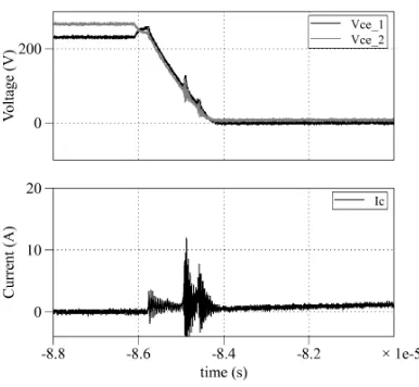
The low side switch was switched twice using a double pulse test method. The first pulse was applied to increase the load current to the desired value. After some delay, the second pulse was applied to capture the current and voltage transient waveforms at turn-on and turn-off. The gate terminal of the high-side switch was connected to the emitter of IGBT3 to turn off the switch during test. The DC link capacitors were charged up to 600 V. The switching characteristics of the switches were measured and recorded using a Tektronix DPO7104 oscilloscope.
B. Measured Results
The operation of the QAGC circuit was validated from the results of the double-pulse switching test at 600 V as shown in Fig. 15. It can be seen that the proposed gate driver is able to turn on and turn off the series string of IGBTs successfully. Voltages across the two IGBTs in the lower switch (Vce1 andVce2) are well balanced during
TABLE I
INITIALVALUES FORCIRCUITPARAMETERS
Component Value Description
IGBT1,2,3,4 IRG4PC40FD IGBT with anti parallel diode
600V 27A (TO-247AC)
Rgate1 5Ω Main gate resistor
Rg1,2,3,4 100Ω Device gate resistor
Rs1,3 660kΩ Static voltage divider resistor
Rs2,4 600kΩ Static voltage divider resistor
Cs1,2,3,4 5.2 nF Dynamic voltage divider
ca-pacitor
CVR1 0.005018Ω Current viewing resistor
Load 3.5 mH Inductive load
Zener
diodes
1N4744 15V zener diode
0 50 100 150 200 250 300
0 5 10 15 20 25
0 50 100 150 200 250
IC
Vce2
Vce1
Volta
ge (
V) Cur
re
nt (
A)
[image:16.612.194.413.110.512.2]Time (us)
Fig. 15. Measured waveforms of a double-pulse test atVdc= 600 V
The close-up views of the waveforms in Fig. 16 show the transient behaviour of the switch during turn off and turn on. The waveforms agree well with the theoretical operation in section II. Although a delay of 150 ns is present at the beginning of the voltage transient, an interdependent turn off mechanism of the QAGC circuit is able to trim the delay down to less than 80 ns. The voltage rising and falling rate is controlled by the capacitorsCs1 andCs2
effectively so that a very good dynamic voltage sharing for both turn-on and turn-off operations can be obtained and no device suffers from a voltage overshoot.
0 50 100 150 200 250 300 Time (us) 0 5 10 15 20 25 0 Volta ge ( V) C ur re nt ( A)
1 2 3 4
Ic Vce2 Vce1 (a) 0 50 100 150 200 250 300 Time (us) 0 5 10 15 20 25 0 Volta ge ( V) C ur re nt ( A)
1 2 3 4
Ic
Vce2
Vce1
[image:17.612.192.423.69.224.2](b)
Fig. 16. close-up view of switching waveforms atVdc= 600 V andIload= 17 A (a) during turn off (b) during turn on
Vce2 Vce1 0 50 100 150 200 250 300 0 Volta ge ( V)
4 8 12 16
Time (us) (a) Vce2 Vce1 0 50 100 150 200 250 300 0 Volta ge ( V)
4 8 12 16
Time (us) (b) Vce2 Vce1 0 50 100 150 200 250 300 0 Volta ge ( V)
4 8 12 16
Time (us) (c) Vce2 Vce1 0 50 100 150 200 250 300 0 Volta ge ( V)
4 8 12 16
Time (us)
[image:17.612.132.484.257.396.2](d)
Fig. 17. Measured device voltages when switching off at (a)Vdc= 600 V (b)Vdc= 500 V (c)Vdc= 400 V (d)Vdc= 300 V
tail current can be distributed through a balancing network in a similar manner to the leakage current.
Fig. 17 compares the voltages across IGBT1 and IGBT2 during turn-off operation at several DC link voltages. It shows that the maximum voltage difference is less than 40 V regardless of what the operating voltage is. This verifies that the circuit is able to provide a balance voltage sharing to the series string.
This suggests that enough gate charge have been transferred to the upper IGBT and confirms that a proper choice of components has been selected. Fig. 18 compares the performance for a range of values ofCs. It shows that the
gate voltage will stay at just above the gate plateau voltage if Cs is made too small as in the case of Fig. 18(a)
where 2.2 nF capacitors were used. The gate voltage Vge2 can rise to nearly 15 V withCs of 5.2 nF.
VI. CONCLUSION
Vge2
Vge1
-15 -10 -5 0 5 10 15
Volta
ge (
V)
Time (us)
0 1 2 3 4 5 6 7 8 9
(a)
Vge2
Vge1 -15 -10 -5 0 5 10 15
Volta
ge (
V)
Time (us)
0 1 2 3 4 5 6 7 8 9
[image:18.612.168.449.70.190.2](b)
Fig. 18. Measured device gate voltages when switching on atIload= 21 A andVdc= 600 V (a) Cs = 2.2nF (b) Cs = 5.2nF
A matched dynamic voltage behaviour is achieved resulting in a well balanced voltage between the devices. Further improvements have been suggested to allow the circuit to be used with an extended number of power devices in the series string. The modified circuit make it possible to implement in high-power semiconductor modules.
The QAGC circuit is attractive in term of simplicity and a small number of component count. Therefore, it is easy to integrate the circuit and the standard gate driver together.
REFERENCES
[1] E. Carroll, S. Linder, I. Blidberg, and A. Chekmarev, “High power semiconductors in the world of energy management,” inRussian
Electrical Engineering, vol. 78, no. 10, 2007, pp. 515–518.
[2] K. Jong-Hyun, M. Byung-Duk, S. V. Shenderey, and R. Geun-Hie, “High Voltage Pulsed Power Supply Using IGBT Stacks,”Dielectrics
and Electrical Insulation, IEEE Transactions on, vol. 14, no. 4, pp. 921–926, 2007.
[3] W. Hongfang, A. Q. Huang, and W. Fei, “Development of a Scalable Power Semiconductor Switch (SPSS),”Power Electronics, IEEE
Transactions on, vol. 22, no. 2, pp. 364–373, 2007.
[4] S. J. Finney, B. W. Williams, Green, and T. C, “RCD Snubber Revisited,”IEEE transactions on industry applications., vol. 32, no. 1, pp.
155–, 1996.
[5] C. Gerster, “Fast high-power/high-voltage switch using series-connected IGBTs with active gate-controlled voltage-balancing,” inApplied
Power Electronics Conference and Exposition, 1994. APEC ’94. Conference Proceedings 1994., Ninth Annual, 1994, pp. 469–472 vol.1.
[6] F. Bauer, L. Meysenc, and A. Piazzesi, “Suitability And Optimization Of High-voltage Igbts For Series Connection With Active Voltage
Clamping,” vol. 20, no. 6, pp. 1244–1253, 2005.
[7] B. Kim, H.-J. Ju, K.-C. Ko, and E. Hotta, “Active clamping circuit to suppress switching stress on a mos-gate-structure-based power
semiconductor for pulsed-power applications,”Plasma Science, IEEE Transactions on, vol. 39, no. 8, pp. 1736 –1742, aug. 2011.
[8] B. Ju Won, Y. Dong-Wook, and K. Heung-Geun, “High-voltage switch using series-connected IGBTs with simple auxiliary circuit,”Industry
Applications, IEEE Transactions on, vol. 37, no. 6, pp. 1832–1839, 2001.
[9] C. Abbate, G. Busatto, and F. Iannuzzo, “High-Voltage, High-Performance Switch Using Series-Connected IGBTs,”Power Electronics,
IEEE Transactions on, vol. 25, no. 9, pp. 2450 –2459, sept. 2010.
[10] R. Withanage and N. Shammas, “Series Connection of Insulated Gate Bipolar Transistors (IGBTs),”Power Electronics, IEEE Transactions
on, vol. 27, no. 4, pp. 2204–2212, 2012.
[11] W. Yalan, P. R. Palmer, A. T. Bryant, S. J. Finney, M. S. Abu-Khaizaran, and L. Gangru, “An Analysis of High-Power IGBT Switching
Under Cascade Active Voltage Control,”Industry Applications, IEEE Transactions on, vol. 45, no. 2, pp. 861–870, 2009.
[12] I. Baraia, J. A. Barrena, G. Abad, J. M. Canales, and U. Iraola, “An experimentally verified active gate control method for the series
connection of igbt/diode-s,”Power Electronics, IEEE Transactions on, vol. PP, no. 99, p. 1, 2011.
[13] P. Evans, N. Teerakawanich, and C. M. Johnson, “Active control of series connected, voltage driven power devices using a single gate
[14] H. L. Hess and R. J. Baker, “Transformerless capacitive coupling of gate signals for series operation of power MOS devices,”Power
Electronics, IEEE Transactions on, vol. 15, no. 5, pp. 923–930, 2000.
[15] R. Guidini, D. Chatroux, Y. Guyon, and D. Lafore, “Semiconductor power mosfets devices in series,” inPower Electronics and Applications,
1993., Fifth European Conference on, sep 1993, pp. 425 –430 vol.2.
[16] J. Dodge, “Eliminating parasitic oscillation between parallel MOSFETs,”Application Note, APT-0402Rev A, 2004.
[17] N. Teerakawanich and C. M. Johnson, “Oscillation Analysis of an Active Gate Control Circuit for Series Connected IGBTs,” inPower
Electronics and Motion Control Conference and Exposition (EPE-PEMC 2012), Proceedings of the 2012-15th International Conference
on, 2012, pp. 1 –6.
[18] T. Lim, B. Williams, S. Finney, and P. Palmer, “Series-Connected IGBTs Using Active Voltage Control Technique,”Power Electronics,
![Fig. 9.Root loci when Rg varies from 10 ohms to 50 ohms showing the minimum value of Rg required to keep the complex eigenvalues inthe LHS of the s-plane [17]](https://thumb-us.123doks.com/thumbv2/123dok_us/8698569.381071/11.612.218.399.74.228/varies-showing-minimum-value-required-complex-eigenvalues-plane.webp)