Room-temperature Operation of Low-voltage, Non-volatile,
Compound-semiconductor Memory Cells
Ofogh Tizno1, Andrew R. J. Marshall1, Natalia Fernández-Delgado2, Miriam Herrera2, Sergio I. Molina2 and Manus Hayne1
Whilst the different forms of conventional (charge-based) memories are well suited to
their individual roles in computers and other electronic devices, flaws in their properties
mean that intensive research into alternative, or emerging, memories continues. In
particular, the goal of simultaneously achieving the contradictory requirements of
non-volatility and fast, low-voltage (low-energy) switching has proved challenging. Here, we
report an oxide-free, floating-gate memory cell based on III-V semiconductor
heterostructures with a junctionless channel and non-destructive read of the stored data.
Non-volatile data retention of at least 104 s in combination with switching at ≤2.6 V is
achieved by use of the extraordinary 2.1 eV conduction band offsets of InAs/AlSb and a
triple-barrier resonant tunnelling structure. The combination of low-voltage operation
and small capacitance implies intrinsic switching energy per unit area that is 100 and
1000 times smaller than dynamic random access memory and Flash respectively. The
device may thus be considered as a new emerging memory with considerable potential.
Keywords: Storage class memory, III-V, compound semiconductors, InAs/AlSb/GaSb,
resonant tunnelling, low power, non-volatile
1 Department of Physics, Lancaster University, Lancaster LA1 4YB, UK.
memory device with compact form. Exploitation of the spectacular conduction-band line-up of AlSb/InAs for charge retention, and for the formation of a resonant-tunnelling barrier, has enabled us to demonstrate the contradictory characteristics of low-voltage (low-energy) operation and non-volatile storage7. The device is a FG memory structure made of InAs/AlSb/GaSb heterostructures, with InAs used as both FG and the junctionless channel. Simulations are undertaken to demonstrate the device operation concept, while the key memory properties of our device, such as the retention characteristics of the programmed/erased states, are presented as experimental results on fully-operational single cell devices.
Operation concept
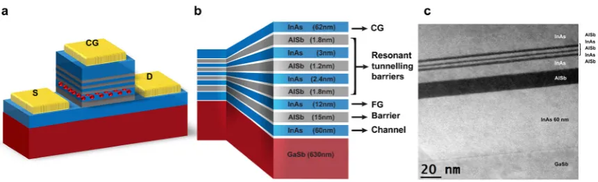
Fig. 1 is a schematic representation of the memory cell, along with a cross-sectional, high-angle, annular, dark-field, scanning transmission electron microscopy (HAADF-STEM) image of the epitaxially-grown material used in this work. Like Flash, charge is stored in a FG. However, there are no oxide barriers. Instead, we have exploited the conduction band offsets in the so-called 6.1-Å family of semiconductors22. Hence, the device underlying the memory
[image:3.595.86.517.74.205.2]cell is more akin to a high-electron mobility transistor (HEMT) than a MOSFET. The channel is formed by InAs that contains neither any junctions nor doping concentration gradients. It is,
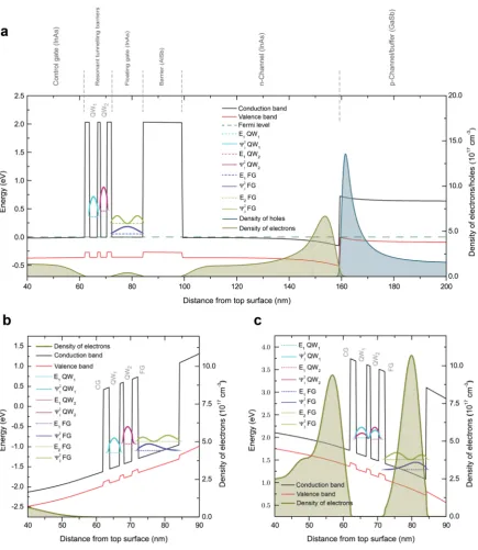
[image:4.595.81.517.122.624.2]however, n-doped to compensate for unintentional background doping and intrinsic Ga vacancies and antisite defects in the underlying GaSb, both of which make the layers naturally p-type23. Fig. 2a depicts the simulated band alignment together with the electron and hole densities within the layers in the absence of bias. As illustrated in the figure, and well documented in the literature22, at the InAs/GaSb interface the InAs conduction band is located below the GaSb valence band, resulting in the flow of electrons from the GaSb into the InAs, and leaving holes in the GaSb. Accumulated electrons/holes can be seen at the InAs/GaSb interface, however, the electrons in the InAs channel are not bound to the InAs/GaSb interface and there is significant electron density throughout the InAs channel. The conductance of the entire channel is dominated by the electrons in the InAs, which will have higher mobility and higher areal density (because of the doping) than the holes in the GaSb. The intrinsic InAs FG is isolated from the InAs channel by a 15-nm AlSb barrier, while double InAs quantum wells (QWs) with triple AlSb barriers serve as a resonant-tunnelling barrier between the FG and the n-doped InAs CG. Hence, in our devices the electrons stored in the InAs FG are isolated by the anomalously-large conduction-band discontinuity with AlSb, a charge-confinement system that was predicted to have a room-temperature thermally-activated storage time of an extraordinary 1014 years24.
In this work, read, write and erase operations were conducted on a number of 10 m × 10 m (gate dimension) cells in an electrostatically-shielded dark box at room temperature. All processes, including write and erase, were executed with ≤2.6 V bias, which is about an order of magnitude lower than is needed to fully operate a Flash cell. Erase was performed by application of a CG bias, 𝑉 , of +2.5 or +2.6 V between the CG and the source, resulting in a “0” state. Fig. 2b shows the calculated band alignments resulting from applying an erase voltage of +2.6 V. Under such circumstances, the calculated electron energy level in QW1 is
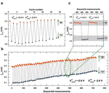
[image:7.595.80.519.279.653.2]Figure 3 | Erase-read-write-read cycles. “0” and “1” states are prepared by application of erase and write voltages, 𝑉 and 𝑉 , respectively, and read via the source-drain current, IS-D, with
1.0 V bias across the channel and zero bias on the control gate. a, Single read measurements subsequent to each erase or write. b, Part of an extended measurement with multiple reads (every 1 s)following each erase or write operation (>80 cycles shown). c,A detail of a portion of the data in b showing a slight convergence of IS-D for “0” and “1” states following erase and write. In b and c
lower than the level in QW2, while both are below the first excited-state and close to the ground-state energy level in the FG. Furthermore, the calculated electron probability density for the ground state in the FG predicts a high electron accumulation at the interface with the resonant-tunnelling barrier and a decaying tail extended into the first AlSb barrier (on the left). The net effect of an erase is thus an electron flow from the FG to the CG, depleting the FG. Similarly, write used 𝑉 𝑉 to increase the charge in the FG (a “1” state). Fig. 2c shows the calculated band diagram when a CG bias of 𝑉 = −2.6 V is used to write the data. In this case, the energy levels in QW1 and QW2 are nearly coincident, leading to a strong coupling of these states, resonant tunnelling, and electron flow from the CG to the FG, charging the FG.
Due to capacitive coupling, the conductivity of the channel depends on the amount of charge stored in the FG, so data is read by measuring the source-drain current, IS-D, for fixed source-drain voltage, VS-D. A “1” state, defined as increased charge in the FG, reduces the charge in the channel, hence its conductivity. Conversely, a “0” state increases the channel conductivity. The data can be read in the absence of any bias to the CG, but such a voltage would be required to select individual devices (bits) in an array of cells, and should generate an electric field across the resonant-tunnelling barrier that is insufficient to allow the passage of charge into or out of the FG. Applying ~2.5 V between the CG and a common back gate can conveniently achieve this.
Memory characteristics
following each write or erase. This clearly demonstrates the non-destructive nature of the read operation. A clear differentiation between the “0” and “1” states is maintained throughout both sequences, although in Fig. 3b there is an undesirable, but almost symmetric, upward drift in
IS-D as the number of operations increases. The reason for this requires further investigation, but is likely to be an asymmetry in the write-erase process, such that each erase removes slightly more charge from the FG than the write delivers. There is no such drift in Fig. 3a, where the write/erase voltages are slightly lower. Following several hundred write and erase operations and many more reads, in different experiments, there was no sign of damage to the device. Research is currently underway into automated characterisation of endurance of single cell devices, and into defining suitable architectures and operational processes for arrays of memory cells.
evaluations suggest a CG-FG capacitance of the order of 10-12 F for a 10 µm × 10 µm (gate dimension) device, and a switching energy of ~2×10-12 J. Shrinking the device dramatically decreases this number, such that the switching energy is of the order of 10-17 J for the 20 nm node, which is 100 and 1000 times smaller than for DRAM and Flash respectively25. This potential for ultra-low switching energy in an emerging memory is, to the best of the authors’ knowledge, unique.
Retention
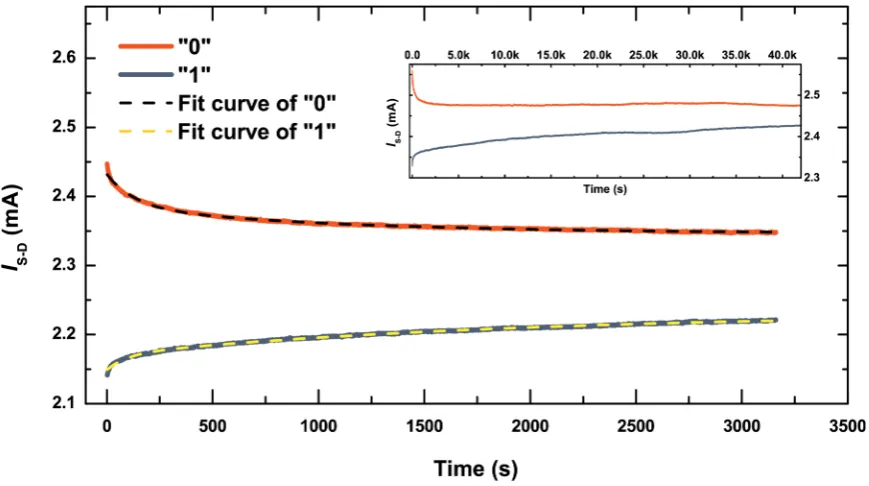
[image:10.595.82.517.73.316.2]successive read operations over extended periods for each memory state. Examples of such measurements are shown in Fig. 4, where the retention characteristics of the memory cells were studied by monitoring their time-dependent behaviour at a constant VS−D = 1.0 V. For this purpose, a read was performed every second for about an hour following an erase pulse (VECG−S = +2.6V, pulse duration 1.0 s). After this experiment, the memory was programmed to the “1” state by a write voltage pulse, (VWCG−S = −2.6V, pulse duration 1.0 s) and the data was read in the same way. Both “0” and “1” states exhibit an initial rapid decay that is consistent with that seen in Fig. 3c. However, for both memory states the initial rapid decay is followed by much slower changes, such that during the entire observation time, the corresponding “0” and “1” states are clearly distinguishable. To further investigate the retention properties of these memory devices, a separate experiment was performed on the same device for an extended period of time. This is illustrated in the inset of Fig. 4, showing the ultimate saturation of the exponential decays and distinct “0” and “1” states over time. Such a storage time is at least 106 times longer than the refresh time required for DRAM.
the applied write/erase voltage, we estimate that write and erase transfer ~107 electrons to or from the FG. Despite the fact that this is a large number, it has a small effect on the conductivity of the laterally-junctionless InAs channel. This is mainly due to the Fermi-level pinning above the conduction band of the highly doped InAs channel which makes it always conductive and very hard to deplete. Furthermore, the InAs channel is 5 times thicker than the FG, leading to a higher level of intrinsic or thermally-generated carriers in this layer. This can be resolved by making the channel thin and narrow enough to allow for full depletion of carriers when the memory is in the “1” state. Strong quantum confinement and, thus, heavy quantisation is expected at sub-20-nm thicknesses26,27.
Conclusions
METHODS
Simulations
The nextnano28,29 software package was utilised for mathematically modelling the energy band diagram of the memory device structure reported here, taking into account strain and piezoelectricity. Within this work, a self-consistent Schrödinger solver was used along with the Poisson and drift–diffusion equations to calculate the electron densities at equilibrium and under bias.
Molecular beam epitaxy
a valved cracker source, the substrate temperature was decreased to 500 °C and a 630-nm-thick GaSb layer was grown. The substrate temperature was further decreased to 440 °C for the growth of the n-type InAs channel (5×1017 cm-3 Si doped). Due to the use of radiative heating in the MBE reactor and an undoped substrate, infrared absorption within the narrow-bandgap epilayer led to an increase in surface temperature to an estimated 470 °C during the growth of the InAs channel. The 15-nm-thick AlSb charge-blocking-barrier layer, the 12-nm-thick InAs floating gate and the AlSb/InAs resonant-tunnelling barrier were grown with InSb-like interfaces to ensure abrupt boundaries between materials and good electrical characteristics31,32. Finally, the control gate was grown with a 7-nm-thick cap layer of intrinsic InAs followed by 55 nm of heavily-doped (1×1018 cm-3 Si) n-type InAs.
Device processing
adhesion between the hydrophobic SiO2 layer and the photoresist, a thin discontinuous layer of Al2O3 was thermally grown on the surface of the sample. However, to get access to the top and back gates, the source and the drain, the oxide layer was chemically etched (using buffered oxide etch, 10:1) in the contact areas, which were exposed through openings in the photoresist provided by UV lithography. A hard-baked positive photoresist lifting layer was then patterned on one edge of the devices by UV lithography. This enabled deposition of continuous contacts, and at the same time, prevented any shorts between the metal and the layers (other than the desired ones) in regions where the oxide was possibly partly over-etched. To form ohmic contacts to InAs (control gate, source and drain) and GaAs (back gate), saturated ammonium polysulphide ((NH4)2S:Sx) was used to remove the native oxide with minimal semiconductor material removal and to passivate the semiconductor surface in the contact areas35. Finally, the metal contacts were formed by deposition of 20/100 nm Ti/Au with an e-beam evaporator.
Electrical measurements
Current-voltage measurements were carried out on individual devices using a dual-channel Keithley 2436B source meter unit. Memory chips were mounted on to a ceramic chip holder, with connections formed by gold wire attached between bond pads and the chip holder. Semi-automated measurements using custom-made software were performed in darkness at room temperature and pressure, with the sample in an electrically-shielded switching box. All measurements reported here were on 10 m × 10 m devices. Erase was performed with 𝑉 of +2.5 or +2.6 V applied between the control gate and the channel, with source and drain grounded, and similarly for write, with 𝑉 𝑉 . Read was performed by measuring
Transmission electron microscopy measurements
A conventional method was used to prepare the specimen in cross section for the analysis by HAADF-STEM. This consisted of mechanical thinning by SiC sandpaper to a thickness of 30 µm, followed by Ar+ milling using a precision ion-polishing system to create a hole. The area suitable for study is located at the edges of the hole. The beam energy during milling has to be controlled carefully to obtain a high-quality electron-transparent sample; 3.5 kV was used at the beginning, and 2 kV at the last step, to get a clean and smooth surface. The HAADF-STEM study was carried out using a JEOL 2010 F at 200 kV.
References
1. Bez, R., Camerlenghi, E., Modelli, A. & Visconti, A. Introduction to flash memory.
Proc. IEEE91, 489–502 (2003).
2. Aritome, S. Nand Flash Memory Technologies. (John Wiley & Sons, Inc., 2015). doi:10.1002/9781119132639
3. Aritome, S., Shirota, R., Hemink, G., Endoh, T. & Masuoka, F. Reliability issues of flash memory cells. Proc. IEEE81, 776–788 (1993).
4. Chen, J. J., Mielke, N. R. & Hu, C. C. Nonvolatile Memory Technologies with Emphasis on Flash. Nonvolatile Memory Technologies with Emphasis on Flash: A Comprehensive Guide to Understanding and Using Flash Memory Devices (John Wiley & Sons, Inc., 2007). doi:10.1002/9780470181355
5. Jacob, Bruce Ng, Spencer W. Wang, D. Memory Systems - Cache, DRAM, Disk. (Morgan Kaufmann Publishers Inc., 2007).
6. Akerman, J. Toward a Universal Memory. Science (80-. ).308, 508–510 (2005). 7. Wong, H.-S. P. & Salahuddin, S. Memory leads the way to better computing. Nat.
Nanotechnol.10, 191–194 (2015).
8. Tian, H. et al. A Dynamically Reconfigurable Ambipolar Black Phosphorus Memory Device. ACS Nano10, 10428–10435 (2016).
9. Zhang, E. et al. Tunable Charge-Trap Memory Based on Few-Layer MoS 2. ACS Nano9, 612–619 (2015).
10. Wong, H.-S. P. et al. Phase Change Memory. Proc. IEEE98, 2201–2227 (2010). 11. Koelmans, W. W. et al. Projected phase-change memory devices. Nat. Commun.6,
12. Guo, R. et al. Non-volatile memory based on the ferroelectric photovoltaic effect. Nat. Commun.4, 1990 (2013).
13. Lee, Y. T. et al. Nonvolatile Ferroelectric Memory Circuit Using Black Phosphorus Nanosheet-Based Field-Effect Transistors with P(VDF-TrFE) Polymer. ACS Nano9, 10394–10401 (2015).
14. Yang, J. J., Strukov, D. B. & Stewart, D. R. Memristive devices for computing. Nat. Nanotechnol.8, 13–24 (2012).
15. Baeumer, C. et al. Spectromicroscopic insights for rational design of redox-based memristive devices. Nat. Commun.6, 8610 (2015).
16. Cappelletti, P. Non volatile memory evolution and revolution. in 2015 IEEE
International Electron Devices Meeting (IEDM)2016–Febru, 10.1.1-10.1.4 (IEEE, 2015).
17. Kwon, K.-C. et al. Nanoscale CuO solid-electrolyte-based
conductive-bridging-random-access-memory cell operating multi-level-cell and 1selector1resistor. J. Mater. Chem. C3, 9540–9550 (2015).
18. Chappert, C., Fert, A. & Van Dau, F. N. The emergence of spin electronics in data storage. Nat. Mater.6, 813–823 (2007).
19. Hu, J.-M., Li, Z., Chen, L.-Q. & Nan, C.-W. High-density magnetoresistive random access memory operating at ultralow voltage at room temperature. Nat. Commun.2, 553 (2011).
20. Freitas, R. F. & Wilcke, W. W. Storage-class memory: The next storage system technology. IBM J. Res. Dev.52, 439–447 (2008).
21. Hayne, M. Improvements relating to electronic memory devices. PCT/GB2015/053191. PCT/GB2015/053191
22. Kroemer, H. The 6.1 Å family (InAs, GaSb, AlSb) and its heterostructures: a selective review. Phys. E Low-dimensional Syst. Nanostructures20, 196–203 (2004).
23. Dutta, P. S., Bhat, H. L. & Kumar, V. The physics and technology of gallium antimonide: An emerging optoelectronic material. J. Appl. Phys.81, 5821–5870 (1997).
24. Nowozin, T., Bimberg, D., Daqrouq, K., Ajour, M. N. & Awedh, M. Materials for Future Quantum Dot-Based Memories. J. Nanomater.2013, 1–6 (2013).
25. Prall, K. Benchmarking and Metrics for Emerging Memory. in 2017 IEEE International Memory Workshop (IMW)6, 1–5 (IEEE, 2017).
26. Bleszynski, A. C. et al. Scanned probe imaging of quantum dots inside InAs nanowires. Nano Lett.7, 2559–2562 (2007).
27. Takei, K. et al. Quantum confinement effects in nanoscale-thickness InAs membranes.
Nano Lett.11, 5008–5012 (2011).
28. Birner, S. Modeling of Semiconductor Nanostructures and Semiconductor-electrolyte Interfaces. (Technischen Universität München, 2011).
30. Craig, A. P., Carrington, P. J., Liu, H. & Marshall, A. R. J. Characterization of 6.1Å III–V materials grown on GaAs and Si: A comparison of GaSb/GaAs epitaxy and GaSb/AlSb/Si epitaxy. J. Cryst. Growth435, 56–61 (2016).
31. Spitzer, J. et al. Quality of AlAs‐like and InSb‐like interfaces in InAs/AlSb superlattices: An optical study. Appl. Phys. Lett.62, 2274–2276 (1993).
32. Shiralagi, K., Shen, J. & Tsui, R. Effects of layer design on the performance of
InAs/AlSb/GaSb resonant interband tunneling diodes on GaAs substrates. J. Electron. Mater.26, 1417–1421 (1997).
33. Nam, P., Tsai, R., Lange, M. & Deal, W. Shallow mesa isolation of AlSb/InAs HEMT with AlGaSb buffer layer using inductively coupled plasma etching. Proc. Int. Conf. Compd. Semicond. Manuf. Technol. (GaAs Mantech) 3–6 (2005).
34. Sun, J. & Kosel, J. Room temperature inductively coupled plasma etching of InAs/InSb in BCl3/Cl2/Ar. Microelectron. Eng.98, 222–225 (2012).
Acknowledgements This work was partly supported by the Engineering and Physical Sciences Research Council, UK, in the framework of an impact acceleration account and by IQE plc. OT acknowledges the support of an overseas PhD scholarship from the Faculty of Science and Technology, Lancaster University, and from the Joy Welch Educational Charitable Trust. This work was also supported by the Junta de Andalucía (PAI research group TEP-946). HAADF-STEM measurements were taken at DME-SCICyT-UCA.
Author contributions O.T. designed, optimised and performed the device processing and conducted all experiments and simulations. M. Hayne conceived and supervised the research. A.R.J.M. performed the sample growth and advised on the processing. O.T., A.R.J.M and M. Hayne designed the epitaxial layers and wrote the manuscript. M. Herrera, N.F. and S.I.M performed the HAADF-STEM.
Author information
Data availability: Reprints and permissions information is available at
www.nature.com/reprints. The datasets used in generating the figures are available at
https://dx.doi.org/10.17635/lancaster/researchdata/275. Competing interests: The authors declare no competing interests. Correspondence and requests for materials should be addressed to M.H. ([email protected]).