Abstract— Interdigitated Back Contact (IBC) solar cell has been routinely fabricated with efficiencies exceeding 20 %. However, due to the requirements of high- resolution alignment and multiple patterning layers, the IBC manufacturing costs are still high. In contrast, screen printed IBC solar cell is based on inexpensive processes utilizing conventional solar cell equipment. Although the screen printed IBC solar cell is easier to fabricate; however its efficiency is poor. In this paper, the performance constraints on screen printed IBC solar cell based on conventional aluminum metallic diffusion paste were investigated. Two-dimensional modeling was carried out using technology computer aided design (TCAD) tool of the commercial software from SILVACO. Critical process and device parameters impacting IBC solar cell performance including fabrication, configuration and material properties. With suitable starting material, device configuration, and fabrication process, solar cell efficiency as high as 19% has been predicted. Higher efficiency is achievable with boron doping, however, aluminum metallic paste is chosen due to the fabrication simplification which will lead to inexpensive manufacturing.
Index Term— IBC, Interdigitated back contact, Silicon solar
cell, Two-dimension solar cell model.
I. INTRODUCTION
It is well known that the efficiency of conventional silicon solar cell is limited by front surface shadow and series resistive losses. Ideally, the front grid contact and the busbar of conventional silicon solar cell must be minimized to reduce shadowing losses. Unfortunately, reducing the contact grid and busbar dimensions increases ohmic resistive losses. Also, the series resistance issues extend to solar modules where many solar cells are interconnected, this decreasing efficiency of module as well. The tabbing size for solar cell interconnection in module fabrication is limited by the busbar size. Larger tabbing width will produce bigger shadowing losses. Thicker tabbing may create stress during cell interconnection, thus affecting yield [1].
The IBC solar cell has all its contacts located at the rear side. Therefore, there is no trade off between shadowing and resistive losses. Shadowing losses are eliminated resulting in higher photocurrent. The finger and busbar dimensions can
now be significantly increased to reduce resistive losses. All these factors contribute to high conversion efficiency as demonstrated by large area IBC modules [2]. Moreover, cell interconnection becomes simpler since the solar cells can be connected in co-planar configuration. Other advantages include higher packing density resulting in a smaller module footprint for the same output in comparison with conventional module. Finally, with its uniform black/dark appearance IBC module is attractive for building integration.
As with other high efficiency structures, a major disadvantage of IBC solar cell is its complicated fabrication process. In IBC solar cell fabrication, a number of process steps and mask levels are needed. For example, separate process and masking steps are used to precisely define physically separate emitter, base, emitter contact and base contact regions. The precise alignment required for the above processes makes the fabrication process slower and expensive. As a result, the IBC solar cell is often fabricated using four to six lithography steps [3]. Lithography is an expensive process and hard to automate. Reducing lithography steps in the fabrication process makes an economic sense [4]. In addition, lithographically-defined emitter and base regions have other disadvantages as well. They require expensive metallization process such as vacuum evaporation or sputtering beam to define the metal contacts.
Recent work has exhibited strong trend towards lithography-free fabrication process of IBC solar cell [5]. These widely different methods include the use of dielectric with laser ablation combined with screen printing [6], diffusion barrier paste [7, 8], diffusion paste [9] and laser scribing [10]. In terms of terminology, these techniques can be broadly categorized under the term “ screen printed IBC” as the majority of the methods use screen printing for metal contact. While some of these methods have exhibited reasonable efficiency; others exhibit performance far below than the lithographically defined process. The reduced performance of screen printed IBC solar cell could be attributed to several factors including low lifetime, un-optimized device configuration, low shunt due to leakage, and high series resistances.
The objective of this paper is to investigate the potential of screen printed IBC solar cell by modifying conventional solar Mohd K. Mat Desa1,2, Mohd Y. Sulaiman1, Kamaruzzaman Sopian1, Suhaila Sepeai1, Ayu Wazira Azhari1,3
and Saleem H. Zaidi11
1-Solar Energy Research Institute, National University of Malaysia, 43600 Selangor, Malaysia 2-School of Electrical & Electronic Engineering, USM, Nibong Tebal, 14300 Pulau Pinang, Malaysia.
3-School of Environmental Engineering, Universiti Malaysia Perlis, 01000 Perlis, Malaysia.
Optimization of p-type Screen Printed
fabrication process based on Aluminum back surface field (BSF). In this paper, effect of doping processes, device configuration, and starting materials will be addressed. To aid this investigation, TCAD tools from SILVACO were employed . TCAD tools were selected due to their ability to simulate two-dimensional (2D) and three-dimensional (3D) configurations. IBC solar cell structure has interdigitated grid of the p- and n-doped regions on the rear surface. This configuration creates both vertical and lateral movement of photo-generated carriers, therefore 2D simulation capability is needed [11-13].
The work presented in this paper has been divided into three parts. The first part is focused on the fabrication process. In fabrication process, the doping profiles of the Front Surface Field (FSF), Emitter, and Base doping were investigated. The second part is focused on optimization of the geometrical configuration of the screen printed IBC solar cell. In this part, performance variation as a function of emitter fraction, base fraction, and emitter-based separation were investigated. The third part examined material characteristics including minority carrier lifetime, bulk doping, and wafer thickness.
II. DEVICE MODEL AND PARAMETERS
A. Base Unit Cell Structure and Parameters
The TCAD tools consist of two separate programs; Athena and Atlas. Athena allows simulation of 2D and 3D configurations. Relevant semiconductor fabrication processes such as diffusion, ion implantation and etching can be modeled. Atlas, on the other hand, is a device simulator. It allows simulation of the electrical, optical and thermal behavior of semiconductor devices [14]. Results in Atlas can be represented as graphical plots such as photogeneration, doping profile, IV response, and electric potentials. The overview of simulation process is described in Fig. 1.
Although there are many papers covering simulation of IBC solar cell, many of the models do not represent low cost device. Most of the simulation models use boron dopants for base region and back surface field (BSF) formation. Boron provides a superior p+ region and BSF, however, it does not conform with the conventional screen-printed IBC. The boron diffusion process, not only requires very high temperature, its application needs masking layers as well, therefore making fabrication process more challenging and difficult. The model presented here uses Aluminum (Al) or a mixture of Silver and Aluminum (Ag/Al) pastes to provide p+ dopants and create the BSF.
IBC model presented here is represents extension of the work of Baraona [11], Hacke [7] and Meier [15]. A common feature of their IBC solar cells was diffusion of metallic contact. Diffusion of metallic contact is an attractive concept because of the simplification it brings to the manufacturing process; it is also a standard process in conventional solar cell manufacturing. In this concept, ohmic contact as well as dopants are introduced together and are self-aligned. Therefore, the fabrication steps are reduced resulting in elimination of the alignment process. At present, only Aluminum is used widely as the self-doping base contact. The
use of Aluminum as diffusion metallic paste is well-established in literature [13, 16-19].
During the IBC solar cell simulation, higher density meshes were placed in high recombination areas including front surface, contacts regions, and the rear surface. This ensures rapid simulation process without compromising performance accuracy. The starting material used was p-type with substrate resistivity of 2 Ω·cm and a thickness of 200 µm; unit size length was 3000 µm. A p-type wafer was chosen since it is readily available and inexpensive. P-type wafers are also widely used in the Si solar cell industry, which can lead to rapid transition to industrial manufacturing [20]. Same methodology can be applied to n-type wafers, and will be reported in the future.
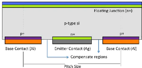
The modeled screen-printed IBC is schematically described in Fig. 2. The emitter or n+ regions and front surface field (FSF) layer (floating junction) were created by phosphorous implantation. The uses of floating junction instead of FSF simplify the fabrication process since it can be formed simultaneously with emitter in phosphorous Trichloride (POCl3) furnace. Floating emitter helps passivate the front surface and reduces carriers recombination by preventing minority carriers to flow to the surface [21].
The emitter metal contact was Ag. The contact dimension was chosen to be 1-mm wide, although finer contact dimension is desirable in order to reduce carrier recombination near the contact region. For the base region, Al was selected for the contact as well as dopant source. Al provides p+ dopants that were self-aligned to the base contact width. The use of Al enables an evaluation of the performance of a low-cost and simplified IBC structure.
Isolation between emitter and base region can be achieved by many methods including laser ablation or etching. Alternatively, isolation can be achieved with the help of diffusion barrier prior to emitter diffusion. In an actual device, the choice of isolation will has a strong influence on the performance because it determines the shunt resistance. In this IBC model, isolation between emitter and base regions was assumed perfect. Other simplifications made in the model include finite ohmic contact resistance and planar front surface (no texturing).
model [14]. An AM1.5 light was used to generate photo response of the solar cell.
III. RESULTS AND DISCUSSION
A. Doping Concentration of Front Surface Field, Base and Emitter
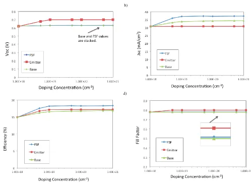
The objective of these simulations is examine how the doping profile influences the performance of screen printed IBC. Figure 5 plots the response of the open circuit voltage (Voc), current density (Jsc), Efficiency and Fill Factor as a function of the doping concentration of the emitter, base and FSF regions. At each point the doping concentration corresponding to other three regions are maintained the same. Figure 5 (a) plots the Voc against the doping concentration. It is observed that Voc increases until it levels off after the doping concentration in the emitter reaches 1x1019cm-3. Sufficient doping of emitter is required to form built up potential in junction region. The Voc is however not affected by changes in concentrations of the base and FSF.
In contrast, current density, Jsc, increases significantly with the increase in the front surface field doping as seen in Fig. 5 (b). The significant effect of the front surface field is due to the high number of photogenerated carriers generated near the front surface as seen in Fig. 4. The electric potential created by the FSF layer repels minority carriers, which reduces the front surface recombination velocity [13]. The Jsc also increases with increase in the base doping concentration. The base doping creates a BSF that reduces the carrier recombination at the rear side [24], which is beneficial especially for a back contact structure in which all the photo-generated carriers created at the front surface are collected at the rear side.
From Fig. 5 (c), it can be inferred that the cell efficiency was dominated by the FSF doping. The efficiency increase is also appreciable with base doping; this effect is least impacted by emitter doping. Therefore, achieving good FSF doping is essential for superior performance of the IBC solar cell. Figure 5 (d) shows that the fill factor of the solar cell is barely influenced by doping concentration of the FSF and base doping. There is only slight increase in fill factor due to the surface field created on the front surface, BSF, and emitter region. The fill factor of the cell is related to the bulk doping and contact resistance. Since bulk doping and contact resistance are fixed; no appreciable variation in fill factor was observed.
Doping process also enhances conductivity of a semiconductor. This is requirement for formation of ohmic contacts to emitter and base regions. Doping concentration of 1x1019 cm-3 corresponding to 0.002 Ω /square/ or lower are necessary for ohmic contacts. However, overdoping increases recombination, creates a dead layer reducing the cell response to short wave photons [25].
B. Geometrical Design of Cell
1) Pitch Dimension
The pitch of the cell is the size from emitter to emitter contacts or the equidistance between similar patterns that comprise the cell (Fig. 6). A smaller pitch results in finer
pattern. The pitch size also determines the methods used for fabrication of the solar cell. Finer pitch requires a photolithography-based pattern resolution, whereas larger pitch allows more versatile, inexpensive equipment such as screen printing. In this paper, pitch dimension was varies in order to examine the effect on the solar cell output performance.
Fig. 7 plots the efficiency of the IBC solar cell with increasing pitch dimension. The pitch size effect can be described in terms of electrical shading [26]. If minority carriers are generated above the base region, the carriers have to travel in vertical and lateral dimension to be collected at the nearest emitter region. Increasing the pitch size increases the lateral dimension of the carrier. As a result the minority carriers have to travel a longer distance before being collected. Some of these carriers might recombine due to longer traversing distance before being collected. This will reduce the carrier collection, therefore reducing the efficiency of the devices as the pitch is increased.
2) Emitter Fraction
The emitter fraction is the percentage of the emitter region over the base plus the compensation regions on the backside. The emitter of the solar cell is where the photogenerated carriers are separated. In theory, a larger emitter area results in larger junction area, and thus, more photogenerated current can be collected. In this structure, we vary the emitter region and fix the base region. Higher emitter fraction and smaller pitch size reduce the effect of electrical shading. Fig. 8 plots efficiency with respect to emitter fraction variation. As expected, a larger emitter faction results in higher efficiency of the IBC solar cell
C. Material Properties
1) Minority Carrier Lifetime
Minority carrier lifetime is the duration within which a photogenerated carrier will recombine. The lifetime τ of minority carrier is equal to the number of generated carrier Δη over the recombination rate, R (please see Eq. 1). The bulk lifetime of wafer τbulk is the sum of the radiation lifetime τrad , auger lifetime τauger and SRH lifetime τsrh as described in Eq. 2. For indirect bandgap such as silicon, the influence of τauger and τsrh is more significant. The τauger increases as doping or impurity introduces to silicon material are reduced while τsrh is related to the defect in the crystal structure of the material. The lifetime is also an indication of diffusion length Ln, of minority carrier according to Eq. 3 where D is diffusivity of silicon material. Ln determines how far the minority carrier travels before they recombine.
(1)
(2)
Placing all the contacts to the rear side not only changes the physical configuration of the device but also the way it functions. In IBC solar cell, the junction or emitter region is located at the rear side in an interdigitated arrangement with the base region. Therefore, photogenerated carriers have to travel through the bulk before they are collected by the emitter and base region contacts. The photogenerated carriers have a greater chance of recombining in IBC solar structure. The importance of good passivation [27], [28] and FSF [13, 29] to reduce recombination have been discussed previously.
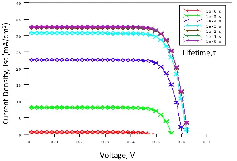
Simulation results in Fig. 9 show that for poor minority carrier lifetimes, the majority of the photogenerated electron-hole pairs recombine before reaching the contacts. As lifetime increases, the VOC, JSC, and efficiency also increase accordingly with greater gains in the current density. However the gains are less substantial as the lifetime increases to more than 1e-4 s, which suggests that as long as the wafer has sufficient minority carrier lifetime for electron-hole pairs to reach the rear side contacts, the efficiency of the IBC solar cell will remain satisfactory.
2) Wafer Thickness
The cost of Si material is significant in solar cell manufacturing. In industrial Si solar cells, Si thickness is currently in the range 150 µm to 200 µm based on existing wafering capabilities [30]. Innovative cleaving techniques capable of producing thickness in the range of 10 µm to 50 µm exist, but such thin wafers require special handling that cannot be obtained with conventional screen printing methods [31].
To obtain an insight on how the thickness of the wafer influences the performance of screen-printed IBC solar cell, screen-printed IBC with varying thicknesses is evaluated. Two sets of simulations were performed. The first set of simulations was for high carrier minority lifetime wafer and the second set for low minority carrier lifetime wafer. The effect of thickness on high and low quality substrates is examined. Using diffusivity of silicon as 27cms-2, lifetime of 1 ms and 10 s corresponded to diffusion length of 164 m and 1643 m (Eq. 3) for low and high lifetime wafers. For wafers of lifetime 1 ms, the highest efficiency is 15 %, as shown in Fig. 10, corresponding to 250 and 300-m thicknesses. With decreasing thickness, the efficiency is slightly reduced due to the presence of less Si substrate to capture all the incident photons. Therefore, some of the light going into the Si is not absorbed because of the less bulk region. Higher wavelength of light, such as photons near the infrared region, confirm this tendency. The effect can be reduced by employing good anti-reflective coating and light trapping such as texturing.
For the low lifetime wafers, the highest efficiency cell is 10.55 % corresponding to a thickness of 20 m. As thickness increases to 50 m or higher, there is significant drop in efficiency even though this thickness is within the diffusion length of minority carriers. The drop in efficiency is due to the shorter diffusion length of the photogenerated carriers, which leads to recombination of most of the carriers before they can
be collected at the rear side. In general, diffusion length of three times the wafer thickness is required for sufficient carrier collection.
For screen printing applications, the current wafer thickness in the market is adequate as long as the carrier lifetime is reasonable. A wafer with thickness below 200 m is fragile and susceptible to cracking during screen printing and handling processes.
3) Wafer Bulk Doping
Another important wafer characteristic is its bulk doping level. Impurities such as P, B, or arsenic are added to reduce the resistivity and defined the type of the semiconductor. However, increased impurity level degrades the electronic properties of silicon. Increasing dopant concentrations reduce minority carrier lifetime because of the increase in SRH and Auger recombination [25]. Figure 11 illustrates that the poorest performance of a IBC solar cell is from a low resistivity substrate exhibiting an efficiency of less than 1 %. As resistivity increases, gain in efficiency is observed. Considering the data in Fig. 11, an optimum efficiency can be achieved for substrate resistivity of about 5 Ω·cm. Within this resistivity, edge recombination can be suppressed [32]. For higher resistivity substrate, the efficiency decreases because of lower fill factor attributed to higher bulk resistivity.
4) Aluminum and Boron dopants.
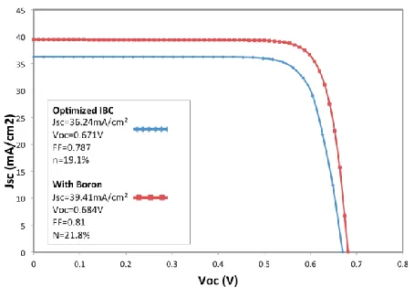
With an optimized doping process, device configuration, and wafer material properties, an efficiency of 19.1 % screen-printed IBC solar cell is achievable. Considering the planar front surface, an efficiency gain of more than 20% would be expected if the front surface was textured. Interestingly, when Boron was used to replace Aluminum dopants for the base contact, a higher efficiency was obtained as seen in Fig. 12. To investigate this effect further, profiles of Aluminum and Boron concentration were examined as shown in Fig. 13. The Aluminum doping profile has very shallow high concentration dopant region at around 0.5 μm thick. As depth increases, there was very steep decline of aluminum concentration with depth. On the other hand boron profile exhibits much deeper high concentration region of about 1.2 μm. Boron doping profile exhibits less steeper decline in concentration with depth resulting in deeper diffusion profile. Part of the reason of shallower aluminum doping profile is the larger particle size of Aluminum compared to Boron. Boron with smaller particle size can diffuse deeper with silicon.
Fig. 14 plots the surface potential of Boron and Aluminum dopants. It can be seen that although Aluminum produces higher surface potential, the field is very shallow and concentrated near the surface region. Boron dopant in the other hand created much deeper electric potential. This results in more effective BSF than Aluminum hence higher efficiency device. The superior performance of Boron than Aluminum is well-established in literature [16].
enhanced by mixing with Boron [33]. In the study Boron was added to Aluminum metal paste to provide better BSF in conventional silicon solar cell. Therefore, this technique can be applied to screen printed IBC solar cell as well.
IV. CONCLUSION
In this paper, a 2D model of screen-printed IBC solar cell has been investigated. The model was based on Aluminum metallic paste diffusion. A detailed analysis based on doping concentration, device configuration and wafer material characteristics was carried out. Achieving an optimal doping profile of FSF, emitter, and base doping is critical to highest performance. Regarding the pattern configuration, the limit will depend on screen printing accuracy since fine pitch and higher emitter fraction are desirable for better IBC performance. Regarding the starting material, high minority carrier lifetime is perhaps the most critical factor dictating the performance of IBC. With optimized solar cell parameters, an efficiency of 19% can be achieved for an inexpensive, screen printing-based solar cell. Efficiency is, in part, limited by the metallurgy of Aluminum when diffused with Si. Aluminum and Boron co-diffusion could further enhance efficiency; further research is required. In summary, Aluminum provides simplified fabrication process exhibiting performance good enough for industrial manufacturing.
ACKNOWLEDGEMENT
The authors would like to thank Solar Energy Research Institute staff for access to SILVACO software.
REFERENCES
[1] E. V. Kerschaver and G. Beaucarne, "Back-contact solar cells: a review," Progress in Photovoltaics: Research and Applications, vol. 14, pp. 107-123, 2006.
[2] M. A. Green, K. Emery, Y. Hishikawa, W. Warta, and E. D. Dunlop, "Solar cell efficiency tables (version 40)," Progress in Photovoltaics: Research and Applications, vol. 20, pp. 606-614, 2012.
[3] G. Jiun-Hua and J. E. Cotter, "Interdigitated backside buried contact solar cells," in Photovoltaic Energy Conversion, 2003. Proceedings of 3rd World Conference on, 2003, pp. 1463-1466 Vol.2.
[4] M. J. Cudzinovic and K. R. McIntosh, "Process simplifications to the Pegasus solar cell - SunPower's high-efficiency bifacial silicon solar cell," in Photovoltaic Specialists Conference, 2002. Conference Record of the Twenty-Ninth IEEE, 2002, pp. 70-73. [5] S. H. Lee, "Cost effective process for high-efficiency solar cells,"
Solar Energy, vol. 83, pp. 1285-1289, 2009.
[6] E. Van Kerschaver, S. De Wolf, and J. Szlufcik, "Towards back contact silicon solar cells with screen printed metallisation," in Photovoltaic Specialists Conference, 2000. Conference Record of the Twenty-Eighth IEEE, 2000, pp. 209-212.
[7] P. Hacke and J. M. Gee, "A screen-printed interdigitated back contact cell using a boron-source diffusion barrier," Solar Energy Materials and Solar Cells, vol. 88, pp. 119-127, 2005.
[8] S. De Wolf, G. Agostinelli, Allebe, x, C., E. Van Kerschaver, and J. Szlufcik, "Selective junction separation techniques for multi-crystalline silicon solar cells," in Photovoltaic Specialists Conference, 2002. Conference Record of the Twenty-Ninth IEEE, 2002, pp. 320-323.
[9] J. Salami, B. Cruz, and A. Shaikh, "Diffusion Paste Development for Printable IBC and Bifacial Silicon Solar Cells," in Photovoltaic
Energy Conversion, Conference Record of the 2006 IEEE 4th World Conference on, 2006, pp. 1323-1325.
[10] F. J. Castano, D. Morecroft, M. Cascant, H. Yuste, M. W. P. E. Lamers, A. A. Mewe, I. G. Romijn, E. E. Bende, Y. Komatsu, A. W. Weeber, and I. Cesar, "Industrially feasible 19% efficiency IBC cells for pilot line processing," in Photovoltaic Specialists Conference (PVSC), 2011 37th IEEE, 2011, pp. 001038-001042. [11] C. R. P. Baraona, OH), G. A. B. Mazaris, OH) , and A.-t. N. R.
Chai, OH), "Screen printed interdigitated back contact solar cell," 1984.
[12] D. L. D. Meier, H. P. ; Shibata, A. ; Abe, T. ; Kinoshita, K. ; Bishop, C. ; Mahajan, S. ; Rohatgi, Ajeet ; Doshi, P. ; Finnegan, M., "Self-Doping Contacts and Associated Silicon Solar Cell Structures," in Presented at the 2nd World Conference on Photovoltaic Solar Energy Conversion; Vienna, Austria; July 6-10, 1998., Vienna, Austria, 1998.
[13] G. Chun, E. Van Kerschaver, J. Robbelein, T. Janssens, N. Posthuma, J. Poortmans, and R. Mertens, "Screen-Printed Aluminum-Alloyed Emitter on High-Efficiency N-Type Interdigitated Back-Contact Silicon Solar Cells," Electron Device Letters, IEEE, vol. 31, pp. 576-578, 2010.
[14] Silvaco, "ATLAS user's manual."
[15] D. L. D. Meier, H. P. ; Shibata, A. ; Abe, T. ; Kinoshita, K. ; Bishop, C. ; Mahajan, S. ; Rohatgi, Ajeet ; Doshi, P. ; Finnegan, M., "Self-Doping Contacts and Associated Silicon Solar Cell Structures," presented at the 2nd World Conference on Photovoltaic Solar Energy Conversion; Vienna, Austria, 1998. [16] G. Chun, E. Van Kerschaver, J. Robbelein, N. E. Posthuma, S.
Singh, J. Poortmans, and R. Mertens, "High efficient N-type interdigitated back contact silicon solar cells with screen-printed al-alloyed emitter," in Photovoltaic Specialists Conference (PVSC), 2010 35th IEEE, 2010, pp. 003145-003148.
[17] A. Kalio, A. Richter, M. Hörteis, and S. W. Glunz, "METALLIZATION OF N-TYPE SILICON SOLAR CELLS USING FINE LINE PRINTING TECHNIQUES," Energy Procedia, vol. 8, pp. 571-576, 2011.
[18] J. Krause, R. Woehl, M. Rauer, C. Schmiga, J. Wilde, and D. Biro, "Microstructural and electrical properties of different-sized aluminum-alloyed contacts and their layer system on silicon surfaces," Solar Energy Materials and Solar Cells, vol. 95, pp. 2151-2160, 2011.
[19] C. Jia, Z. H. J. Tey, D. Zhe Ren, L. Fen, B. Hoex, and A. G. Aberle, "Investigation of Screen-Printed Rear Contacts for Aluminum Local Back Surface Field Silicon Wafer Solar Cells," Photovoltaics, IEEE Journal of, vol. 3, pp. 690-696, 2013. [20] J. E. Cotter, J. H. Guo, P. J. Cousins, M. D. Abbott, F. W. Chen,
and K. C. Fisher, "P-Type Versus n-Type Silicon Wafers: Prospects for High-Efficiency Commercial Silicon Solar Cells," Electron Devices, IEEE Transactions on, vol. 53, pp. 1893-1901, 2006.
[21] T. Nagashima, K. Hokoi, K. Okumura, and M. Yamaguchi, "Surface Passivation for Germanium and Silicon Back Contact Type Photovoltaic Cells," in Photovoltaic Energy Conversion, Conference Record of the 2006 IEEE 4th World Conference on, 2006, pp. 655-658.
[22] B. Shu, U. Das, J. Appel, B. McCandless, S. Hegedus, and R. Birkmire, "Alternative approaches for low temperature front surface passivation of interdigitated back contact silicon heterojunction solar cell," in Photovoltaic Specialists Conference (PVSC), 2010 35th IEEE, 2010, pp. 003223-003228.
[23] D. S. Kim, V. Meemongkolkiat, A. Ebong, B. Rounsaville, V. Upadhyaya, A. Das, and A. Rohatgi, "2D-Modeling and Development of Interdigitated Back Contact Solar Cells on Low-Cost Substrates," in Photovoltaic Energy Conversion, Conference Record of the 2006 IEEE 4th World Conference on, 2006, pp. 1417-1420.
[25] M. A. Green, Solar Cells Operating Principles, Technology and System Application vol. 1. Kensington, New South Wales: Prentice Hall, December 1998.
[26] S. Kluska, F. Granek, M. Rüdiger, M. Hermle, and S. W. Glunz, "Modeling and optimization study of industrial n-type high-efficiency back-contact back-junction silicon solar cells," Solar Energy Materials and Solar Cells, vol. 94, pp. 568-577, 2010. [27] J. L. Cruz-Campa, M. Okandan, P. J. Resnick, P. Clews, T. Pluym,
R. K. Grubbs, V. P. Gupta, D. Zubia, and G. N. Nielson, "Microsystems enabled photovoltaics: 14.9% efficient 14μm thick crystalline silicon solar cell," Solar Energy Materials and Solar Cells, vol. 95, pp. 551-558, 2011.
[28] T. M. Razykov, C. S. Ferekides, D. Morel, E. Stefanakos, H. S. Ullal, and H. M. Upadhyaya, "Solar photovoltaic electricity: Current status and future prospects," Solar Energy, vol. 85, pp. 1580-1608, 2011.
[29] D. Diouf, J. P. Kleider, T. Desrues, and P. J. Ribeyron, "Effects of the front surface field in n-type interdigitated back contact silicon heterojunctions solar cells," Energy Procedia, vol. 2, pp. 59-64, 2010.
[30] X. Yu, P. Wang, X. Li, and D. Yang, "Thin Czochralski silicon solar cells based on diamond wire sawing technology," Solar Energy Materials and Solar Cells, vol. 98, pp. 337-342, 2012. [31] J. Kraiem, P. Papet, O. Nichiporuk, S. Amtablian, J. F. Lelievre, S.
Quoizola, A. Fave, A. Kaminski, P. J. Ribeyron, C. Jaussaud, and M. Lemiti, "Elit Process: Epitaxial Layers for Interdigitated Back Contacts Solar Cells Transferred," in Photovoltaic Energy Conversion, Conference Record of the 2006 IEEE 4th World Conference on, 2006, pp. 1126-1129.
[32] R. A. S. P. J. Verlinden, K. Wickham, R. A. Crane and R. M. Swanson, "Backside Contact Silicon Solar Cells with Improved Efficiency for the '96 World Solar Chalenge," in Proc. 14th European PVSEC, Barcelona, Spain, 1997.
[33] X. Gu, X. Yu, and D. Yang, "Efficiency improvement of crystalline silicon solar cells with a back-surface field produced by boron and aluminum co-doping," Scripta Materialia, vol. 66, pp. 394-397, 2012.
[34] M. Wright and A. Uddin, "Organic—inorganic hybrid solar cells: A comparative review," Solar Energy Materials and Solar Cells, vol. 107, pp. 87-111, 2012.
FIGURES
Fig. 1. Modeling IBC solar cell structure process in SILVACO TCAD tools.
IMAGE SIZE: 88 mm/ 181 mm RESOLUTION: 300dpi FONT: Times New Roman
Fig. 2. Cross section of screen printed IBC. The base region was doped with Aluminum dopants to simulate screen printing. Aluminum produces the p+ dopants for the back surface field (BSF) and also acts as the base contact.
Fig. 3. Cross section of unit cells used in the simulation. The unit cell mapped the entire structure by repeating the symmetrical geometry. Symmetrical structure is shown on the left while unsymmetrical structure is shown on the right. Unsymmetrical structure resulted in inaccuracy in the representation of the whole
structure.
IMAGE SIZE: 88 mm/ 181 mm RESOLUTION: 300dpi FONT: Times New Roman
LABEL: (a) (b) , combined with image IMAGE: Combine all images into one
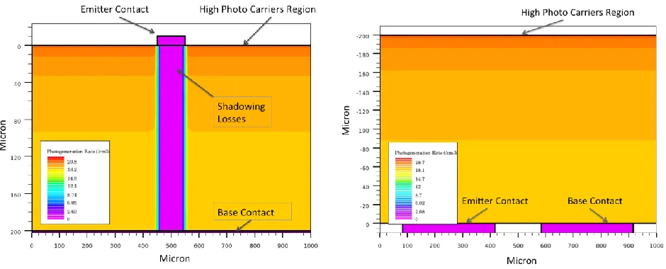
Fig. 4. Photogenerated carriers density in an IBC and conventional screen printed (left) solar cell during illumination. Highest fractions of photogenerated carriers are located near the front surface. Shadowing losses can be observed in SP conventional solar cell.
IMAGE SIZE: 88 mm/ 181 mm RESOLUTION: 300dpi FONT: Times New Roman
a) b)
c) d)
Fig. 5. Variation of (a) Voc, (b) Jsc, (c)Efficiency and (d) Fill factor of Front Surface Field, Base and Emitter doping as a function of the doping concentration.
IMAGE SIZE: 88 mm/ 181 mm RESOLUTION: 300dpi FONT: Times New Roman
LABEL: (a) (b) (c) (d), combined with image IMAGE: Combine all images into one
Fig. 6. Rear view of IBC solar cell. Low pitch (left) and high pitch (right) structures of the IBC solar cells.
IMAGE SIZE: 88 mm/181 mm RESOLUTION: 300dpi FONT: Times New Roman
Fig. 7. Variation of efficiency of IBC solar cell for different pitch dimensions. As the pitch size is reduced, the probability of carrier collection increases resulting in higher efficiency cell.
IMAGE SIZE: 88 mm/181 mm RESOLUTION: 300dpi FONT: Times New Roman
Fig. 8. Variation of efficiency of IBC solar cell for different emitter fractions. Bigger emitter fraction results in higher efficiency IBC solar cell.
IMAGE SIZE: 88 mm/181 mm RESOLUTION: 300dpi FONT: Times New Roman
Fig.9. LIV response of IBC solar cells as function of minority carrier lifetime. As the lifetime increases more photo generated carriers have higher chances to be collected.
Fig. 10. IBC solar cells efficiency against wafer thickness. For high lifetime wafer, increasing the thickness results in increased efficiency. On the other hand, poor carrier lifetime wafer would result in reduced efficiency as the thickness is increased due to limited diffusion length, Ln.
IMAGE SIZE: 88 mm/181 mm RESOLUTION: 300dpi FONT: Times New Roman
Fig. 11. IBC solar cell efficiency against substrates base resistivity. Selection of a good base substrate resistivity will ensure good performance IBC solar cell.
IMAGE SIZE: 88 mm/181 mm RESOLUTION: 300dpi FONT: Times New Roman
Fig. 12. Shown above is the IV curve of IBC solar cell with optimized doping, geometrical and substrates (red). This is compared to similar structure but with boron as dopant for base region (blue).
Fig. 13. The doping profile of Aluminum dopants (left) and boron dopants [34]. Aluminum dopant shows shallower profile with high concentration near the surface region.
IMAGE SIZE: 88 mm/181 mm RESOLUTION: 300dpi FONT: Times New Roman
LABEL: (a) (b) , combined with image IMAGE: Combine all images into one FIGURE AXIS LABEL
Fig. 14. The electric potential on the base region from Aluminum dopants (left) and boron dopants [34]. Boron dopants show much deeper electric potential compare to aluminum dopants.
IMAGE SIZE: 88 mm/181 mm RESOLUTION: 300dpi FONT: Times New Roman
TABLE I
SOLAR CELL PARAMETERS USED FOR SIMULATION OF SCREEN PRINTED IBC SOLAR CELL
Serial No.
Parameters Value
1. Wafer Thickness 200µm
Type p-type
Resistivity Width
2Ω.cm 3000µm
2. Front Surface Field Dopants Phosphorous
(Floating Junction) Concentration Varied
3. Emitter Dopants Phosphorous
Concentration Varied
Width 1000µm
4. Back Surface Field (BSF) Dopants Aluminum
Concentration Varied
Width 1000µm
5. Back Surface Recombination
Velocity (BSRV)
Value 1000cm/s
6. Front Surface Recombination
Velocity(SRV)
![Fig. 13. The doping profile of Aluminum dopants (left) and boron dopants [34]. Aluminum dopant shows shallower profile with high concentration near the surface region](https://thumb-us.123doks.com/thumbv2/123dok_us/1366076.1646161/11.612.49.547.363.561/profile-aluminum-dopants-dopants-aluminum-shallower-concentration-surface.webp)
