A Hardware Prototype of a Flexible Spectrum
Sensing Node for Smart Sensing Networks
∗
Ahmed Elsokary
1,*, Peter Lohmiller
1, Václav Valenta
1and Hermann Schumacher
11UlmUniversity,InstituteofElectronDevicesandCircuits,Albert-Einstein-Allee45,89081Ulm,Germany.
Abstract
In this paper we present a prototype for a spectrum sensing node for a cognitive radio sensing network. Our prototype consists of a custom down-conversion front-end with an RF input frequency range from 300 MHz to 3 GHz and a Power Spectral Density (PSD) estimation algorithm implemented on a Virtex-6 Field Programmable Gate Array (FPGA). The base-band processing part is capable of calculating the PSD for a bandwidth upto 245.76 MHz achieving a resolution of 60 kHz and an online variable averaging functionality with a maximum of 32767 averages. We show the arithmetic optimization techniques used for the PSD evaluation to optimize FPGA resource usage. Real time performance and calculation of the PSD for real world signals in the GSM downlink, DECT and the UHF DVB-T bands are demonstrated.
Receivedon 14 May, 2015;acceptedon 24 November, 2015;publishedon 05 April, 2016
Keywords: Spectrum Sensing, Multiband, Cognitive Radio, FPGA Implementation, Hardware Prototype, Periodogram, PSD, FFT
Copyright© 2016 AhmedElsokaryetal.,licensedto EAI.Thisisanopen accessarticledistributedunderthetermsof theCreativeCommonsAttributionlicense(http://creativecommons.org/licenses/by/3.0/),whichpermitsunlimited use,distributionandreproductioninanymediumsolongastheoriginalworkisproperlycited.
doi:10.4108/eai.5-4-2016.151143
1. Introduction
Cognitive Radio (CR) is an appealing concept for solving the spectrum resource scarcity problem caused by the current static allocation of frequency bands [2][3]. In this context, the Primary User (PU) is the licensed user with priority to use a frequency channel. A Secondary User (SU) is a cognitive user who can reuse frequency white spaces that are channels unused by PUs. Once a PU transmission is detected, the SU must leave the used frequency band immediately to avoid interference. A key requirement for the CR concept is a reliable spectrum sensing [4] with the aim of robust PU detection.
Multiband spectrum sensing deals with the detection of multiple white spaces simultaneously. The main advantage is the quick detection of PUs and offering multiple opportunities to the SU. An important decision metric for multiband detection is the Power Spectral
∗
This paper is an extended version of a manuscript presented at the 10th International Conference on Cognitive Radio Oriented Wireless Networks (CROWNCOM), 2015 [1] where section 3 was modified to includearithmeticprecisionselection.Implementationresultsona lowercostFPGAfamilywereappendedtosection4.
*
Corresponding author. Email:[email protected]
Density (PSD), that describes the average density of the power distribution within the detection bandwidth.
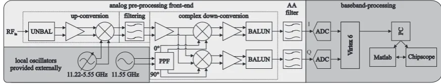
This paper deals with design, implementation and experimental deployment of a spectrum sensing node prototype. The future goal is the hardware implementation of a multiband distributed spectrum sensing network, where cooperative detection takes place between all nodes. Each node contains a flexible front-end and a bank of sensing algorithms for decision evaluation. The realized sensing node in this paper consists of a customized RF front-end and a PSD evaluation implemented on a Field Programmable Gate Array (FPGA). The system diagram is shown in Fig.1.
The main goal is the optimization of the sensing speed and the evaluation in practical scenarios. Our prototype shows a sensitivity of -107 dBm and a bandwidth of 245.76 MHz with a frequency resolution of 60 kHz. Economic use of target FPGA resources was achieved through optimization of arithmetic and memory operations. The RF front-end covers an RF input frequency range from 300 MHz up to 3 GHz. The flexibility in the hardware prototype is achieved through the reconfiguration of parameters such as averaging and windowing in real time, and a tunable external local oscillator to select the target frequency
Figure 1. Frontend connected to the base-band processing.
band during operation. The prototype is tested and verified in realistic scenarios.
2. PSD Evaluation
The PSD is evaluated by averaging over several periodograms. This reduces the estimation error as more averages are taken [5]. The periodogram is the squared magnitude of the Discrete Fourier Transform (DFT) of the received signal. The L-point DFT of a discrete time domain vector x of length L is calculated as follows:
Xk=
L−1
X
n=0 x(n)
−j2πnk
L , k= 0,1, ..., L−1. (1)
A window function is used to reduce spectral leakage, on the other hand it degrades the frequency resolution. Different window functions that offer different trades between resolution and leakage reduction are available [6]. In this paper, we use the Blackman window as it offers the highest sidelobe suppression. The modified periodogram calculation becomes
Xk=
L−1
X
n=0
w(n)·x(n) −j2πnk
L , k= 0,1, ..., L−1, (2)
wherewis the window function of size L. The PSD is estimated by
ˆ
P = 1
Navg Navg−1
X
m=0
|Xˆ |2m, (3)
where
|Xˆ |2m=Re{Xˆm}2+Im{Xˆm}2, (4)
ˆ
X={X0, X1, X2, ...XL−1}.
This is a special case of the Welch estimator described in [5] where there is no overlap between the time domain signals used to calculate the averaged periodograms.
3. Implementation Methodology
This section discusses the implementation of the PSD evaluation on the FPGA and the performed optimization to operate at the target clock frequency while choosing the precision to achieve a high sensitivity. In this section, D refers to the complex data path between the consecutive arithmetic blocks.F
denotes complex signals that get stored in a First In First Out (FIFO) memory. Complex in this context implies the concatenation of the real and imaginary parts of the signal. Each block is enabled by a 1-bit signalen, it issues a signalvalidwhen it starts to stream its output into the following block. L refers to the Fast Fourier Transform (FFT) size andNavg refers to the number of
calculated spectral averages. A delay ofmclock cycles is denoted byz−m.
3.1. Main Building Blocks
A block diagram of the calculation is shown in Fig. 2. The DFT is practically realized using the FFT. A window function is applied to the FFT to reduce spectral leakage. The FFT is followed by magnitude evaluation and reordering that performs the bit reversed indexing of the FFT output to show the PSD in natural order of the frequency bins. This is followed by averaging of the calculated PSD for a user selected number of averages. The implementation is done in VHDL with generic parameters for each module for PSD calculation. This enables manual optimization and achieving an improved performance on the FPGA. Xilinx ISE 14.5 was used for synthesis and bit file generation for the FPGA.
Figure 2. Block diagram for PSD evaluation.
3.2. Fast Fourier Transform
An FFT was designed based on the radix-22 architec-ture. The radix-22 algorithm introduced in [7] offers a
simple butterfly structure similar to the radix-2 algo-rithm and a low number of multipliers similar to the
2
EAI Endorsed Transactions on Cognitive Communications 122015 - 03 2016|Volume2|Issue 6 |e1
EAI
European Allianceradix-4. This technique was used in our design to conserve area and reduce complexity. Single-path Delay Feedback (SDF) architecture is used to reduce the con-trol complexity and memory requirements. The imple-mentation methodology in [8] was used for the FFT implementation, where we use arithmetic optimization and extended pipelining to increase clock frequency. Fig.3shows the block diagram of the FFT.
Figure 3. Block diagram of the FFT unit.
It consists of consecutive stages where each stage comprises two butterfly calculation units (BFI, BFII) and a complex multiplier to carry out the twiddle factor multiplications. Twiddle factors are the complex factors multiplied by the input samples in the DFT calculation. The number of stages r is equal to log
4L. The last
stage does not contain a multiplier and contains only one butterfly (BFI) when the FFT length is an odd power of 2. When the length is an even power of 2, it contains both BFI and BFII.
Butterfly Unit. The difference between the two butterfly
units is the BFII multiplication by −j which is carried
by multiplexers to swap the real and imaginary parts. The structure of BFII is shown in Fig.4. The selection lines to the multiplexers from the control unit choose the samples that are multiplied by−j.
Figure 4. Butterfly unit BFII.
Twiddle Factor Multiplication. The twiddle factors were
pre-calculated and stored in ROMs on the FPGA. A MATLAB script was written to write the ROM initialization file for a generic FFT length and precision. The method for the pre-calculation was mentioned in [8]. Each stage k has a ROM of size N /22k. The
implemented complex multiplier for that purpose is shown in Fig. 5. The complex multiplier was fully
pipelined to achieve a minimum critical path delay. The real multipliers need three pipeline levels.
Figure 5. Twiddle factor multiplier implementation.
3.3. Reordering Unit
The reordering unit was designed according to the methodology shown in [9]. The design uses consecutive stages each with a memory feedback for reordering. It achieves a lower clock cycle delay than direct reordering schemes that use simple storing in a RAM and manipulating the read address.
3.4. Magnitude Evaluation Unit
This unit was realized by two multipliers and an adder, for performing addition of the squared real and imaginary parts of the calculated FFT according to Eq. (4).
3.5. Averaging Unit
An array accumulator was designed to perform the spectral averaging while streaming the input PSD frames continuously. The control structure is shown in Fig.6. The first counter of size log2Lcounts the output PSD points. The second counter of size log2Navg,max
counts the number of accumulations. Resetting the FIFO is accomplished by adding 0 to the incoming frame to replace the current stored accumulation value.
The critical path delay introduced by the large adder was reduced using a conventional technique described in [10]. It is achieved by replicating the feedback path into two partial accumulators and pipelining them through the carry bit. It was used in our design where the registers in the partial accumulators were extended to FIFO buffers in the feedback, where each FIFO stores half of the bits of the accumulated PSD frame. In Fig.7, an example of the structure for a 4-bit accumulator is given.
Figure 7. Pipelined averaging to reduce the adder critical path delay.
3.6. Arithmetic Operations
In the baseband subsystem, a dual channel 14-bit ADC [11] was used for data conversion. This finite accuracy introduces quantization noise to the system. In order to optimize the FPGA utilization of the PSD evaluation, truncation of the internal calculations was performed. The internal FFT bit size had to be selected to have minimal degradation regarding sensitivity and quantization noise while using the available FPGA resources optimally. The magnitude evaluation and averaging were done at full precision to conserve the sensitivity.
The software model of the implemented FFT was used to evaluate the necessary number of bits to accommodate the full dynamic range of the used ADC while using truncation of the internal calculations to optimize the FPGA utilization.
The slot noise test (used to evaluate the Xilinx FFT IP-core in [12]) was performed on the fixed point software model of the system to verify the effect of the arithmetic format used for our FFT. In the slot noise test, a time domain signal is generated that has non-zero values over all of its spectral components except for a small number of consecutive bins called the slot. This procedure is shown in Fig. 8. Ideally, performing the FFT on this input signal should yield a zero for the slot bins [12]. However, due to the effect of ADC quantization as well as the high peak to average ratio of such signals, noise appears in the slot band.
This test is used to determine the number of bits necessary so as to not further degrade the performance after the ADC quantization. The result for the test using different bit size configurations is shown in
Figure 8. Slot noise test procedure - the bit size for the fixed-point FFT is increased until no further performance gain is noticeable in the calculated power spectrum.
Fig. 9. We notice that the performance is worse for the 18 bit internal bit size, which degrades the slot noise by approx. 25 dB. The degradation is reduced by increasing the FFT bit size. The performance of the 25 bit internal bit size is similar to that of a floating point FFT for a 14 bit ADC, and no significant improvement could be achieved by further increasing the internal FFT bit size for the same number of ADC bits. Therefore, a 25-bit accuracy was chosen for the FFT calculations.
FFT bin
0 500 1000 1500 2000 2500 3000 3500 4000
P/dBm
-150 -140 -130 -120 -110 -100 -90 -80 -70 -60 -50
18 bits 20 bits 22 bits 25 bits floating point
Figure 9. Slot noise test for various internal FFT bit size configurations, 14-bit ADC, power normalized to a 50Ω input resistance, slot size = 150 bins. A size of 25 bits for the FFT internal calculations achieves the least slot noise compared to a floating point implementation. Magnitude evaluation and averaging are implemented with full precision to avoid any performance degradation.
A test that uses a single tone input with an amplitude equal to the ADC full scale of 2Vpp is done to determine the effect on the quantization noise floor. The result is shown in Fig.10. We notice no significant degradation of the noise floor due to the additional quantization by the FFT calculations. The input signal for the floating point and the fixed point models is
4
EAI Endorsed Transactions on Cognitive Communications 122015 - 03 2016|Volume2|Issue 6 |e1
EAI
European Alliancequantized by 14-bits to model the quantization effect of the ADC.
FFT bin
0 500 1000 1500 2000 2500 3000 3500 4000
P / dBFS
-160 -140 -120 -100 -80 -60 -40 -20 0
floating point 25-bit fixed point
Figure 10. Software model test on a single tone, 14-bit ADC. The power is normalized to the ADC full scale, Blackman window is used. Two peaks are visible corresponding to the frequency of the real valued input single tone. The quantization noise floor is dominated by the ADC. No significant degradation due to the finite precision arithmetic is visible.
The arithmetic operations were optimized by exploit-ing the upper bounds for the expected intermediate calculations for the economic use of the arithmetic resources. The fixed point format [13] was used for the representation of the signal values. The notation
Q(1, i, f) refers to a fixed point format where the
num-ber is a signed numnum-ber and i bits are assigned to the integer part andf bits to the fractional part.
Fig.[11-13] show the format used for the window function, butterfly additions and twiddle factor multi-plications, respectively. The operatortr(n) refers to the truncation ofnLeast Significant Bits (LSBs). A division by 2 to avoid overflow was realized by a shift-right after the butterfly addition. The multipliers on the target FPGA operate on 25×18 bit operands [14]. Therefore,
a bit size of 25 bits was chosen for each of the real and imaginary parts of D to use an optimum number of multipliers achieving the desired sensitivity.
Figure 11. Number format for the window function multiplication.
Fig.14 shows the format used for the squaring and accumulation operations.sxt(n) refers to sign extension by nbits. No truncation is performed to preserve the sensitivity. Therefore, the implemented accumulator needs a sign extension by log2(Navg,max+ 1) bits to avoid
overflow.
Figure 12. Number format for the butterfly additions.
Figure 13. Number format for the twiddle factor multiplication.
Figure 14. Number format for magnitude evaluation and accumulation.
3.7. Memory Optimization
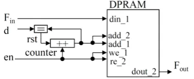
To realize large depth FIFO buffers in the data path, the buffer implementation was optimized to achieve a low routing delay on the FPGA. As using a large number of slice registers results in high routing path delay, RAM resources were used instead. The idea was mentioned in [15] as a RAM based shift register.
For each buffer, a Dual Port RAM (DPRAM) was used with custom manipulation of the read and write address for the two ports to realize a FIFO functionality. A read before write scheme was used for the RAM implementation. Fig. 15shows the control scheme for the addresses for the two RAM ports, where d is the desired FIFO depth.
Figure 15. Realization of a FIFO memory using RAM
4. Sensing Node
4.1. Analog Front-end
300 MHz to 3 GHz into the base-band. The dedicated front-end relies on external local oscillator sources and provides a base-band bandwidth of 100 MHz per I and Q channel. A detailed description of the analog front-end is given in [16]. For all the real world tests, a discone omni-directional antenna (frequency range 300 MHz to 3 GHz) was connected to the front-end. The front-end is followed by a dual channel Analog to Digital Converter (ADC) on the FMC150 evaluation board that provides the digital input of I and Q channels for the Virtex-6 FPGA.
4.2. Base-band Processing
The block diagram of the base-band processing for the implemented prototype is shown in Fig. 16. The Chipscope software communicates with the Integrated Logic Analyzer (ILA) [17] and Virtual Input Output (VIO) [18] Xilinx cores. A software interface was written to control Chipscope from MATLAB to update VIO with the user options for averaging and windowing, and to visualize the output in real time.
Figure 16. Block diagram for base-band processing for the sensing node.
The communication speed between the FPGA and the PC was the bottleneck for the update rate (approx. 1 s) to the PC due to the JTAG interface used by Chipscope. However, this only affects the data display update rate and not the calculation speed, as some calculated data has to be discarded to cope with the limited communication buffer size. In a real system, the communication between the sensing nodes can be implemented with a higher data throughput than JTAG to assist decision making speed.
4.3. Overview of the Hardware Results
The detection performance is shown in Table 1. The target clock frequency is 245.76 MHz to operate in streaming mode from the ADC. For the FFT size of 4096, the Place And Route (PAR) process estimated a maximum clock frequency of 262 MHz for the used Virtex-6 FPGA.
The FPGA resource utilization is shown in Table 2. The low usage of the DSP48E1 slices is a result of the
Table 1. Detection performance
Parameter Value
fs 245.76 MHz
Resolution 60 kHz
FFT size 4096
Calculation time
/clock cycle 10204 + 4096×N avg
fclk,max(PAR.) 262 MHz
performed arithmetic optimization. The RAM resources were used to realize the ROM units used for storing the twiddle factors, and to realize large delays in the data path for optimum performance. The RAM resources used for buffering the output data to the PC are not shown. In Table 3, the resource utilization and the maximum frequency are shown for implementation on the lower cost Artix-7 FPGA. The achievable clock frequency is 220 MHz. The design uses a higher portion of the Artix-7 FPGA since it has lower resources. This shows that the design is suitable for implementation on a lower cost platform. However, the ADC sampling frequency would have to be reduced by 30 MHz which would impact the baseband detection bandwidth.
Table 2. Design FPGA resource utilization (map results)
Resource Number
used
Utilization(%) XC6VLX240T-1 DSP48E1 slices 26 3.3
RAM36K RAM18K
25 15
6 1 Logic Slices 1496 4
Table 3. FPGA resource utilization and clock frequency for the low cost Artix-7 FPGA
Result Value
(XC7A100T-1) DSP48E1 slices 26 (10%) RAM36K
RAM16K
27(20%) 13(4%) Logic slices 1520 (15%)
fclk,max(PAR.) 220 MHz
4.4. Comparison with Other Prototypes
Comparison with two other published platforms that use an FPGA based calculation of the PSD for spectrum sensing is shown in Table 4. Our design achieves superior performance regarding sensing bandwidth and calculation time. In [19], an extra overhead for using a soft processor core for control on the Spartan-6 FPGA and streaming from a low frequency ADC could
6 EAI Endorsed Transactions
on Cognitive Communications 122015 - 03 2016|Volume2|Issue 6 |e1
EAI
European Alliancehave affected the detection time. Compared to [20], the use of custom arithmetic units and memory functions in this work helped to achieve a higher performance.
Table 4. Comparison with existing platforms
Platform fclk (MHz)
bandwidth (MHz)
resolution (kHz)
calculation time(ms) This work 245.76 245.76 60 0.042 + 0.017Navg
[19] 12.8 12.8 25 0.54(Navg=10)
[20] 125 62.5 122 N/A
5. Real Time Testing
5.1. Detection of DVB-T Signals
The detector was tested in the UHF digital TV band for a bandwidth of 245.76 MHz around a central frequency of 580 MHz. The TV signals in the received bandwidth can clearly be observed as shown in Fig.17.
450 500 550 600 650 700
90 80 70 60 50
P
/
dBm
/
60kHz
Figure 17. PSD output from the FPGA based PSD calculation. A ripple in the noise floor is observed. The calculation is performed using 100 averages.
This measurement is done for Navg = 100. A ripple
in the noise floor can be noticed due to the frequency response of the front-end. This ripple was calibrated by disconnecting the antenna, recording the PSD for 32767 averages and dividing the calculated PSDs by the corresponding noise power for each bin.
The result of that calibration is shown in Fig.18. The three 8 MHz wideband signals at carrier frequencies 482 MHz, 626 MHz and 650 MHz are the DVB-T channels 22, 40 and 43 respectively which are received in the city of Ulm [21]. Image signals due to IQ mismatch can be also seen at 18 dB below the corresponding signal powers. Digital calibration to compensate the IQ mistmatch is a remaining future task.
5.2. Detection of Signals in the Band from 1788 to
2033 MHz
To assess the detection speed, the prototype was tested in the frequency range 1788 to 2033 MHz which
450 500 550 600 650 700 0
5 10 15 20 25 30 35
f / MHz
P
/dB
Figure 18. Calibrated PSD output to achieve a flat noise floor. The calculation is performed using 100 averages. Three TV channels can be observed at 482 MHz, 626 MHz and 650 MHz with their corresponding image signals, with 18 dB image suppression.
contains two known signals which apply frequency hopping; Global System for Mobile communication (GSM) downlink and Digital Enhanced Cordless Telecommunications (DECT) signals.
GSM downlink signals apply frequency hopping with time slots equal to 576.9 µs according to [22]. DECT phone signals in the band from 1880 to 1900 MHz have 5 ms frames [23]. Fig.19shows the spectrogram that is displayed real time from the FPGA calculation.
observation time /s
f
/MHz
0 10 20 30 40 50 60 70 80 90 100 1790
1830
1870
1910
1950
1990
2030
Δ
P
/
d
B
0 10 20 30 40 GSM downlink 21805 B 1879 MHz3
Image signals
DECT phones 21880 B 1900 MHz3
Figure 19. Spectrogram for the band from 1788 to 2033 MHz for a duration 100 seconds. The update rate is 1 PSD measurement /s. GSM downlink signals can be observed as well as frequency hopping of DECT phone signals. Images of DECT phone signals appear due to IQ mismatch
The detection time here is 1.76 ms for Navg =
5.3. Sensitivity
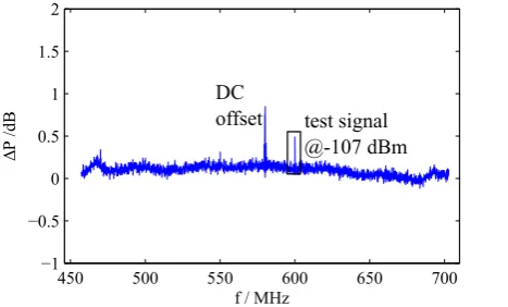
To assess the sensitivity, a sinusoidal signal with adjustable power is connected to the RF front-end’s input. The central frequency was set to 580 MHz. The signal is generated at 600 MHz. It mimics a narrowband low power carrier in the TV band. By taking 32000 spectral averages, the lower bound for detection was -107 dBm. The result is shown in Fig. 20. We can clearly distinguish two peaks, at 580 MHz and 600 MHz respectively. The peak at 580 MHz is due to the DC offset of the ADC.
450 500 550 600 650 700
−1
−0.5 0 0.5 1 1.5 2
f / MHz
Δ
P
/dB test signal
@-107 dBm DC
offset
Figure 20. Sensitivity test on a sinusoidal signal with input power -107 dBm and f = 600 MHz.Navg is set to 32000.
The IEEE 802.22 standard for Wireless Regional Area Networks (WRAN) requires a sensitivity of -107 dBm for a signal within a 200 kHz bandwidth [24]. As the PSD is calculated at a resolution bandwidth of 60 kHz, the system needs to be sensitive to a -112 dBm sinusoidal signal to meet the standard for microphone signals. The sensitivity is limited so far by the fairly high noise figure of the front-end [16], which is due to an unexpected reduced gain in the up-conversion stage as well as due to the losses introduced through the realization into a single module. A future re-design, including a low loss input BALUN as well as a re-design of the high-IF filter is expected to further improve the sensitivity of the system by lowering the front-end noise figure.
6. Conclusion and Future Work
In this paper, the design, implementation and real time testing of a sensing node that calculates the PSD are shown. A MATLAB based interface controls the FPGA design and displays the calculated PSD in real-time. The flexibility of the node is demonstrated for spectrum sensing in different frequency bands with different averaging options. The RF front-end down-converts signals in the range of 300 MHz to 3 GHz to baseband. The achieved baseband detection bandwidth is 245.76 MHz, with a frequency resolution of 60 kHz.
The internal bit size for the PSD calculation is selected to optimize FPGA usage while having a minimal effect of the finite precision arithmetic operations on the detection performance. The detection is tested on UHF TV signals, GSM downlink signals and DECT phone signals. A sensitivity test is performed and the node was able to detect signals at -107 dBm. Future work includes digital IQ mismatch compensation that is needed to cancel the image signals that appear during testing. Moreover, the noise figure of the front-end needs to be lowered in order to achieve a higher sensitivity. More integration is targeted by incorporating the local oscillators in the front-end chip, and implementation of wideband frequency sweeping over the full range of the front-end RF bandwidth. The next step is the decision implementation on FPGA and the deployment of several sensing nodes for evaluation of detection algorithms in collaborative sensing scenarios.
Acknowledgment
This project is partially funded by the German Research Foundation (DFG) under grant no. VA941/1-1.
References
[1] Elsokary, A., Lohmiller, P., Valenta, V. and
Schu-macher, H.(2015) A Hardware Prototype of a Flexible
Spectrum Sensing Node for Smart Sensing Networks. InCognitive Radio Oriented Wireless Networks(Springer International Publishing),Lecture Notes of the Institute for Computer Sciences, Social Informatics and Telecommunica-tions Engineering156, 391–404. doi:10.1007/978-3-319-24540-9_32.
[2] Shin, K.G., Kim, H., Min, A.W. and Kumar, A.
(2010) Cognitive Radios for Dynamic Spectrum Access: From Concept to Reality.IEEE Wireless Communications Magazine, vol. 17.
[3] Valenta, V., Maršálek, R., Baudoin, G., Villegas, M.,
Suarez, M. and Robert, F. (2010) Survey on
Spec-trum Utilization in Europe: Measurements, Analyses and Observations. In Fifth International Conference on Cognitive Radio Oriented Wireless Networks and Commu-nications (CROWNCOM).
[4] Yücek, T.andArslan, H.(2009) A Survey of Spectrum
Sensing Algorithms for Cognitive Radio Applications. IEEE Communications Surveys & Tutorials, vol. 11.
[5] Manolakis, D.G., Ingle, V.K.and Kogon, S.M. (2000)
Statistical and Adaptive Signal Processing: Spectral Esti-mation, Signal Modeling, Adaptive Filtering and Array Processing(McGraw Hill).
[6] Harris, F.J.(1978) On the Use of Windows for Harmonic
Analysis with Discrete Fourier Transform.Proceedings of the IEEE, vol. 66.
[7] He, S. and Torkelson, M. (1996) A New Approach
to Pipeline FFT Processor. In IEEE Parallel Processing Symposium.
8 EAI Endorsed Transactions Cognitive Communicationson
122015 - 03 2016|Volume2|Issue 6 |e1
EAI
European Alliance[8] Cortés, A., Vélez, I., Zalbide, I., Irizar, A. and
Sevillano, J.F. (2008) An FFT Core for
DVB-T/DVB-H Receivers. VLSI Design Doi:10.1155/2008/610420, Hindawi Publishing Corporation.
[9] Garrido, M., Grajal, J. and Gustafsson, O. (2011)
Optimum Circuits for Bit Reversal.IEEE Transactions on Circuits and Systems II: Express Briefs.
[10] Chappell, M.andMcEwan, A.(2004) A Low Power High
Speed Accumulator for DDFS Applications. In IEEE International Symposium on Circuits and Systems ISCAS. [11] 4DSP LLC., USA (2010)FMC150 User Manual.
[12] Xilinx, Inc. (2015)Fast Fourier Transform v9.0 LogiCORE IP Product Guide.
[13] Parhami, B.(2010)Computer Arithmetic: Algorithms and
Hardware Designs(Oxford University Press).
[14] Xilinx, Inc. (2011) Virtex-6 FPGA DSP48E1 Slice User Guide.
[15] Alfke, P. (2008) Creative Uses of Block RAM. White
Paper: Virtex and Spartan FPGA Families, Xilinx.
[16] Lohmiller, P., Elsokary, A., Chartier, S. and
Schu-macher, H. (2013) Towards a Broaband Front-end for
Cooperative Spectrum Sensing Networks. In European Microwave Conference (EuMC).
[17] Xilinx, Inc. (2011)LogiCORE IP ChipScope Pro Integrated Logic Analyzer (ILA)(v1.04a).
[18] Xilinx, Inc. (2011) LogiCORE IP ChipScope Pro Virtual Input/Output (VIO) (v1.04a).
[19] Riess, S., Brendel, J. and Fischer, G. (2013)
Model-based Implementation for the Calculation of Power Spectral Density in an FPGA System. In7th International Conference on Signal Processing and Communication Systems (ICSPCS).
[20] Povalač, K.,Maršálek, R.,Baudoin, G.andŠrámek, P.
(2010) Real-time Implementation of Periodogram Based Spectrum Sensing Detector in TV Bands. In20th Interna-tional Conference Radioelektronika (RADIOELEKTRON-IKA).
[21] Südwestrundfunk (2009) Das Programmangebot in
Baden-Württemberg.
[22] ETSI (1998) Digital cellular telecommunications system (Phase 2+) Physical layer on the radio path: General description. Tech. rep.
[23] ETSI (2013) Digital Enhanced Cordless Telecommunica-tions (DECT) - TR103089 V1.1.1. Tech. rep.
[24] Stevenson, C.R., Cordeiro, C., Sofer, E. and
Chouinard, G. (2005) Functional requirements for