ISSN: 2231-5381
http://www.ijettjournal.org
Page 243
High Speed FIR Filter Based on Truncated
Multiplier and Parallel Adder
Deepshikha Bharti#1,
K. Anusudha
*2#1
Student,M.Tech , Department of Electronics Engineering, Pondicherry University, puducherry, India
#2
Assistant professor, Department of Electronics Engineering, Pondicherry University, puducherry,India
Abstract— High speed Finite Impulse Response filter (FIR) is designed using the concept of faithfully rounded truncated multiplier and parallel prefix adder. The bit width is also optimized without sacrificing the signal precision. A transposed form of FIR filter is implemented using an improved version of truncated multiplier and parallel prefix adder. Multiplication and addition is frequently required in Digital Signal Processing. Parallel prefix adder provides a high speed addition and the improved version of truncated multiplier also provides successive reduction in delay and the components used
Keywords— Digital signal processing(DSP), Truncated
multiplier, Parallel adder, FIR filter. VLSI design.
I.INTRODUCTION
An finite impulse response (FIR) filter is a digital filter that works on digital inputs. A digital filter is a system that performs mathematical operations on sampled, discrete time signal to reduce or enhance certain aspect of that signal. There are two types of digital filter mainly used that are infinite response (IIR) filter and finite impulse response (FIR) filter. Finite impulse response (FIR) digital filter is one of the fundamental components in many digital signal processing (DSP) and communication systems. It is also widely used in many portable applications which requires fast operations. In general the transfer function for a linear, time-invariant, filter can be expressed in Z domain as :
H(z) =
( )( )
=
⋯
⋯ …..(1)
When the denominator part is made equal to unity then the equation becomes for an FIR filter. So the final equation for the FIR filter of order N can be expressed as:
[n] =
[ ] +
[
−
1] +
⋯
+
[
−
]
=
∑
b x[n
−
i]
...
(2)The FIR filter has two basic structures, direct form and transposed form as shown in fig 1.
(a)
(b)
Fig. 1. Structures of FIR filters: (a) Direct form and (b) transposed form
ISSN: 2231-5381
http://www.ijettjournal.org
Page 244
[1]–[7]. In order to avoid multiplier block an FIR filter canalso be implemented as: multiplier less and memory based design.
Multiplier less-based designs are realized with shift-and add Operations and share the common sub operations using canonical signed digit (CSD) recoding and common sub expression elimination (CSE) to minimize the adder cost of MCM [8]–[12]. Some multiplier less based FIR filter designs use the transposed structure to allow for cross-coefficient sharing and tend to be faster, particularly when the filter order is small. However, the area of delay elements is larger compared with that of the direct form due to the range expansion of the constant multiplications and the subsequent additions in the adder block.
Memory-based FIR designs consist of two types of approaches: lookup table (LUT) methods and distributed arithmetic (DA) methods [11]–[12]. The LUT-based design stores in ROMs odd multiples of the input signal to realize the constant multiplications in MCM [11]. The DA-based approaches recursively accumulate the bit-level partial results for the inner product computation in FIR filtering.
Fig 2: Digital filter design stages
An important design consideration for the design of FIR filter is the derivation of filter coefficients and the optimization of the bit widths for filter coefficients, which has direct impact on the area and speed of arithmetic units. Some of the DSP application do not require full precision outputs, in such cases the output can be rounded and truncated to save the area and also to increase the speed of the system. Whereas the total error will not be more than 1 unit in the last place (ulp). In this brief, we present high speed implementations of FIR filters based on the transposed structure in Fig. 1(b) with faithfully rounded truncated multipliers and parallel prefix adder. The faithfully truncated multiplier produces the output results by accumulating all the partial products (PPs) where the unnecessary partial products bits (PPBs) are removed without affecting the final precision of output.
This brief is organized as follow: Section II discusses the derivation of filter coefficients, Section III describes the truncated multiplier , Section IV describes about the paralle prefix adder and Section V describes the experimental results.
II. FINDING THE FILTER COEFFICIENTS
For the design of FIR filter the first step is to find the filter coefficients. The filter coefficients can be calculated in several ways as: window design method, frequency sampling method and paks-McClellan method. The simplest way of designing filter is by using the windowing technique using MATLAB software. The filter coefficients can be calculated as:
……(3)
Filter coefficients can be obtained using any of the windows. Hamming windows are particularly well-suited for this method because of their closed form specifications. Here hamming window is used for the calculation of filter coefficients. The equation for the hamming window is given as:
N =
.
…….(4)Finally the set of windowed impulse response coefficients h[n] is calculated as:
…….(5) For
Where,
hd(n) = desigred coefficients
W(n) = 0.54 +0,46cos
( )
n
h
n
W
n
h
d
ISSN: 2231-5381
http://www.ijettjournal.org
Page 245
Fig 3 : Impulse response of a 8 tap filter using hamming Window
Fig 4 : Magnitude and phase response of 8 tap filter using Hamming window
III. TRUNCATED MULTIPLIER
Parallel multipliers are typically implemented as either carry-save array or tree multipliers. In many computer systems, the (n+n)-bit products produced by parallel multipliers are rounded to n bits to avoid growth in word size. In various DSP application it is not needed to use the full output products of multiplier. As in most of the filter implementation the filter output can also be obtained using only the MSB bits of the multiplier output. This type of implementation will also calculate the filter output faster with less area used. This means a multiplier should be designed which requires less delay and that is possible with the truncated multiplier. In the wireless multimedia world, DSP systems are everywhere. DSP algorithms are computationally intensive and test the limits of battery life in portable device such as cell phones, pocket gadget, hearing aids, MP3 players, digital video recorders and so on. Multiplication is the main operation in many signal processing algorithms hence efficient parallel multipliers is desirable.
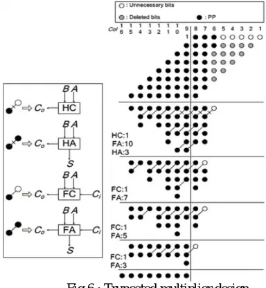
This paper implements a truncation design which decreases the number of used half adders and full adders. The lsb pp do not has much importance in the calculation of final products so these are not calculated which reduced the number of adders in the calculation of products.
Fig 5 : Method of truncation of PPBs
Fig 6 : Truncated multiplier design
In the faithfully rounded FIR filter implementation, it is required that the total error introduced during the arithmetic operations is no larger than one ulp. Fig 5 and fig 6 shows that a considerable amount of ppbs can be deleted leading to smaller area and delay.fig 5 shows a single row of PPBs is made undeletable (for the subsequent rounding), and the PPB elimination consists of only deletion and rounding. The error ranges of deletion and rounding is calculated as follows:
−ulp ≤ ED≤ 0 – ½ulp ≤ ED= ED +– ½ulp ≤– ½ulp −ulp < E_R≤ 0 – ½ulp < ER=ER +– ½ulp≤– ½ulp −ulp < E=(ED + ER) ≤ ulp
1 2 3 4 5 6 7 8 -0.05
0 0.05 0.1 0.15 0.2 0.25 0.3 0.35
Coefficient number
V
a
lu
e
Truncated Impulse Response
0 0.5 1 1.5 2
x 104 -600
-400 -200 0
Frequency (Hz)
P
h
a
s
e
(
d
e
g
re
e
s
)
0 0.2 0.4 0.6 0.8 1 1.2 1.4 1.6 1.8 2
x 104 -60
-40 -20 0
Frequency (Hz)
M
a
g
n
it
u
d
e
(
d
B
ISSN: 2231-5381
http://www.ijettjournal.org
Page 246
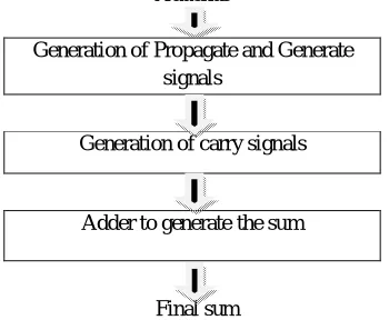
IV. PARALLEL PREFIX ADDERThis paper has used a parallel prefix adder as kogge-stone for the implementation of fir filter. Parallel prefix adder is primarily faster than other carry propagate adder. Parallel prefix adder is the most efficient circuit for the binary addition. kogge-stone adder is a parallel prefix defined form of carry look ahead adder. It generates the carry signal in 0(log n) time, and is widely considered as the fastest adder design possible. It takes more area to implement as compared to others parallel adders but has a lower fan-out at each stages. A parallel Prefix Addition is generally a three step process. The first step implicate the creation of generate (gi) and propagate (pi) signals for the input operand bits. The second step involves the generation of carry signals and finally a simple adder to generate sum. The three stage structure of carry look ahead adder and parallel prefix adder is shown in fig 7.
Addends
Generation of Propagate and Generate signals
Generation of carry signals
Adder to generate the sum
Final sum
Fig 7: Three stage structure of a parallel prefix adder
A kogge-stone type parallel prefix adder precomputes the propagate and generate signal. The propagate signals are obtained by XORing the input bits and the generate signals are obtained by ANDing the input bits. Further these propagate and generate bits are calculated in step by step manner by considering two different types of nodes as black and white nodes. The algorithm for the kogge-stone adder is shown in fig 8.
Fig 8: Design flow of 8 bit kogge-stone adder
The diamond shapes block shows the white notes and the black dot indicated the black nodes. The white nodes (diamond shaped box) is calculated as :
{X[1],y[1]}= {a[1],(a[1]|b[1])&b[0]} …..(6)
The black nodes(black dot) is calculated as:
{x[1],y[1]}={a[1]&b[1],(a[1]|b[1])&b[0]} …..(7)
Both the nodes calculation needs the OR gate and the AND gates Fig 8 shows that, each vertical stage produces a “propagate” and “generate” bit. The culminating generate bit are produced in the last stage (vertical) , and these bits are XOR ‘d with the initial propagate after the input to produce the sum bits.
V. SIMULATION RESULTS
An 8 tap FIR filter using the above truncated multiplier and the parallel prefix adder is implemented. The FIR filter simulation shows considerable reduction in the delay of the filter. For designing of any filter first of all the filter order is selected. Since the main aim of this filter design is to reduce the delay so a low order filter is been chosen for the design. The coefficients for the filter is calculated using MATLAB software. Later the coefficients are stored in the register. Total delay in the design of FIR filter includes that of arithmetic circuit (adder and multiplier) and the delay element (D-flip flop). The structure is been synthesized and simulated using XILINX ISE 13.2 design suit. The following table shows the delay and LUTs used in the calculation of multiplier, adder and the Fir filter.
TABLE I
Arithmetic circuit results
Block Logic delay (ns)
Route delay (ns)
LUTs used
Truncated multiplier
11.372 ns 12.495 ns 91
Parallel prefix adder
8.498 ns 5.619 ns 36
TABLE II
An 8 Tap FIR filter results
Block Logic delay (ns)
Route delay (ns)
LUTs used
Power (mw) 8 Tap FIR
filter, Transposed form
35.11 56.634 1233 3.09
ISSN: 2231-5381
http://www.ijettjournal.org
Page 247
VI. CONCLUSIONThis paper has presented a high speed FIR filter designs by considering the optimization of coefficient bit width and hardware resources in implementations. Although most prior designs are based on the direct form, we observe that the transposed form of FIR filter structure with faithfully truncated multiplier and parallel adder leads to less delay in the calculation of output of FIR filter.
REFERNCES
[1] A. Blad and O. Gustafsson, “Integer linear programming-based bit-level optimization for high-speed FIR filter architecture,” Circuits Syst.signal Process , vol. 29, no. 1. 81-101, Feb. 2010.
[2] S. Hwang, G. Han, S. Kang, and J.-S. Kim, “New distributed arithmetic Algorithm for low-powe r FIR filter implementation,” IEEE Signal
Process.Lett., vol. 11, no. 5, pp. 463–466, May 2004.
[3] H. Samueli, “An improved search algorithm for the design of multiplierless FIR filters with powers-of-two coefficient,” IEEE Trans.
CircuitsSyst., vol. 36, no. 7, pp. 1044–1047, Jul. 1989.
[4] Y. J. Yu and Y. C. Lim, “Design of linear phase FIR filters in subexpression space using mixed integer linear programming,” IEEE
Trans. CircuitsSyst. I, Reg. Papers, vol. 54, no. 10, pp. 2330–2338,
Oct. 2007.
[5] M. M. Peiro, E. I. Boemo, and L. Wanhammar, “Design of high-speed Multiplier less filters using a nonrecursive signed common subexpression algorithm,” IEEE Trans. Circuits Syst. II, Analog Digit.
Signal Process., vol. 49, no. 3, pp. 196–203, Mar. 2002.
[6] F. Xu , C. H. Chang, and C. C. Jong, “Design of low-complexity FIR Filters based on signed -powers -of -two coefficients with reusable common subexpressions,” IEEE Trans. Comput.-Aided Design Integr.
CircuitsSyst., vol. 26, no. 10, pp. 1898–1907, Oct. 2007.
[7] C.H. Chang, J. Chen, and A. P. Vinod, “Information theoretic approach To complexity reduction of FIR filter design, ” IEEE Trans. Circuits
Syst.I, Reg. Papers, vol. 55, no. 8, pp. 2310–2321, Sep. 2008.
[8] F. Xu, C. H. Chang, and C. C. Jong, “Contention resolution—A new Approach to versatile subexpressions sharing in multiple constant multiplications,” IEEE Trans. Circuits Syst. I, Reg. Papers, vol. 55, no. 2, pp. 559–571, Mar. 2008.
[9] F. Xu, C. H. Chang, and C. C. Jong, “Contention resolution algorithms for common subexpression elimination in digital filter design,” IEEE
Trans. Circuits Syst. II, Exp. Briefs, vol. 52, no. 10, pp. 695–700, Oct.
2005.
[10] I.C. Park and H.-J. Kang, “Digital filter synthesis based on an algorithm