A novel majority gate approach for
implementing efficient qca comparator
Tiru Sameer Yarlagadda¹, GSAJ Manikumar²
¹PG Scholar, CEC, ECE Department, AP, India ²Associate Professor, CEC, ECE Department, AP, India
ABSTRACT
A quantum-dot cellular automaton (QCA) was an attractive technology now a days which is used in developing ultra-dense-low-power high-performance digital circuits. Many solutions have been proposed recently for several arithmetic circuits, such as adders, multipliers, and comparators. Nevertheless, since the design of digital circuits in QCA still poses many challenges, novel implementation strategies and methodologies are highly wished for as being an attractive. This paper
put forward a new design approach aligned to the implementation of binary comparators in QCA. New formulations of basic logic equations which are required to perform the comparison function is proposed. The new scheme has been exploited in designing two different comparator architectures and for several operands word length. With comparison to existing counterparts, the comparators proposed in this project exhibit significantly higher speed and reduced overall area.
In The proposed scheme, we deal with 32-bit numbers which have less number of resources unlike conventional comparators, by which the realization of low power and area efficient comparator is designed. This comparator can be used widely in central processing units (CPUs) and microcontrollers.
1. INTRODUCTION
Quantum dot Cellular Automata (QCA)
technology provides a promising opportunity to overcome the approaching limits of conventional CMOS technology. So, in recent years the designs of logic circuits based on QCA have got a great deal of attention, and special efforts have been concentrated towards arithmetic circuits, such as adders, multipliers, and comparators.
EVEN though comparators are main elements in wide range of applications, QCA implementation in the existing literature is mainly provided for comparing two single bits. Only few examples of comparators able to process n-bit operands, with n > 2, are available. The comparator described will simply
computes the XNOR function to decide whether two input bits, a and b matched or not. The structures
proposed will provide higher computational
capabilities, and circuits are able to separately recognize all the three possible conditions in which a = b, a > b, and a < b (here named full comparators) are described. The 1-bit implementation is proposed and then it is improved, exploited, to design a parallel n-bit full comparator. An example of serial structures is shown, whereas the n-bit comparator described and can recognize only the case in which, A and B being the n-bit inputs, A ≥ B. Alternative QCA implementations of 1-bit full comparators were recently proposed. With respect to other QCA designs, the latter exhibit reduced delays, area occupancy and number of used cells.
This paper focuses on the design of efficient parallel QCA-based n-bit full comparators. The main theme of this paper is to introduce a novel design methodology which allows low computational time and very compact layouts to be achieved. In particular, original theorems and corollaries are stated and demonstrated which directly show impact on the QCA realizations of some basic Boolean functions used within the comparator architectures.
The novel theorems are applied to achieve innovative QCA-based structures of n-bit full comparators that lay out and simulated using the QCA Designer tool for n ranging between 2 and 32. As an example, one of the 32-bit comparators designed exploiting the proposed theory was implemented using less than 2800 cells within an overall area of about 2.66 μm2; moreover, it requires only 15 clock cycles to complete the operation.
The rest of the paper is organized as follows: a brief back-ground of the QCA design approach and existing QCA implementations of binary comparators , the new theorems and corollaries are then enunciated and demonstrated ,comparators designed exploiting the novel theorems are proposed in this paper that also presents comparison results with existing designs.
2. QCA BASED COMPARATOR
There are different QCA
comparator take two bits a and b as input and establishes whether they are equal, less than or greater than each other and these possible states are
represented through three output signals, named as Ae q
B, Ab igB, Bb igA, that are asserted, respectively, when a = b, a>b, and a < b. But Full comparators are those that can separately identify all the above cases, whereas non-full comparators recognize just one or two of them. As an example, the comparator designed
which depicted in Fig.1(a) can verify only whether a =
b. And, the rest of circuits shown in Fig.1(b) and (c), proposed, are full comparators. The latter also exploits two 1-bit registers D which are used to process n-bit
operands serially from the least significant bit to the
most significant one.
With the objective of reducing the number of wire crossings, which is still a big challenge of QCA
designs , in the universal logic gate (ULG) f (y1, y2,
y3 ) = M (M (y1 , y2 , 0), M (y1 , y3 , 1), 1)was proposed
and then usedto implement the comparator illustrated
in Fig. 1(d). It worth noting that, two n-bit numbers A(n
−1 :0 ) = an −1 . . . a0 . . . b0 can be processed by
cascading n instances of the 1-bit comparators. As
each instance receives as inputs the ith bits ai and bi (with i = n− 1, . . . , 0) of the operandsand give the signals Ab igB(i−1 :0 ) and Bb igA(i−1 :0 ) . The former is
asserted when the sub word A(i−1 :0 ) = ai−1. . . a0 which
represents abinary number greater than B(i−1 :0 ) = bi−1. . . b0 . In a similar way BbigA(i−1 :0 ) is set to one
when A(i−1 :0 ) < B(i−1 :0 ). The outputs AbigB(i:0 ) and Bb ig A(i:0 ) directly feed the next stage.It can be seen
that this circuit did not identify the case in which A =
B, so it cannot be classified as a full-comparator.
Fig.1: QCA based comparator presented in:
The design described in exploits a tree-based (TB) architecture and exhibits a delay that in theory
logarithmically increases with n. The 2-bit version of
such designed comparator is illustrated in Fig.1(e) Also the full comparator proposed in exploits a TB architecture to achieve high speed. As shown in Fig.1(f), where 4-bit operands are assumed, one instance of the 1-bit comparator presented it is used for each bit position. The intermediate results obtained by this way will further processed through a proper number of cascaded 2-input OR and AND gates implemented by means of MGs having one input permanently set to 1 and 0, respectively. Analyzing existing QCA implementations of binary comparators it can be observed that they were designed directly mapping the basic Boolean functions consolidated for the CMOS logic designs to MGs and inverters, or ULGs. Unfortunately, in this way the computational capability offered by each MG could be underutilized. As a consequence, both the complexity and the overall delay of the resulting QCA designs could be increased in vain.
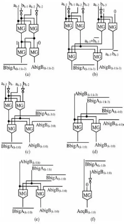
NOVEL QCA COMPARATORS
The comparator which is proposed first will exploits a cascade-based (CB) architecture. To explain better how the overall computation is performed, the schematic diagram illustrated in Fig.1 is provided. It also shows a possible implementation of a 32-bit comparator based on proposed theory. Following the
criterion which is explained in Fig.2, an n-bit CB full
comparator designed as proposed here uses: n/3
instances of T1 and/or T2; n/3 cascaded instances of
T4 by which the signals AbigB(n−1:0) and
BbigA(n−1:0) will be computed; and one instance of
C2, needed to compute also AeqB(n−1:0). Circles
visible in Fig.1 indicate the additional clock phases that have to be inserted on wires to guarantee the correct synchronization of the overall design. The CB full comparator was designed for operands word lengths ranging from 2 to 32 and using, for n > 2, the split criterion summarized in Table I. Obviously, alternative splits could be used.
As it is well known that the number of cascaded MGs within the worst computational path of a QCA design directly affects the delay achieved. In fact, each MG introduces one clock phase in the overall delay. From Fig.1 , it can be seen that the modules T1 and T2 contribute to the computational path with one inverter and two MGs. Each instance of T4 introduces one more MG, whereas C2 is responsible for one MG and one inverter. As a consequence, the critical computational path of the novel n-bit CB full comparator consists of n/3+ 3 MGs and 2 inverters. An example of the 32-bit
implementation depicted in Fig. 2 has the worst-case path made up of 13 MGs and 2 inverters.
Fig 2: Novel 32-bit CB full comparator.
Fig.5: Examples of novel TB comparators with: (a) and (b) 16-bit operands; (c) and (d) 32-bit inputs.
3. PROPOSED ARCHITECTURE
The first proposed architecture presented in based on parallel approach and has two output bits A>B), S( i.e. A<B). The circuit for the 4-bit
comparator is displayed in Fig. 2 and is slightly a modified version of the traditional comparator (which works on bit-weight comparison of two numbers from LSB to MSB) to understand the logic for the proposed architecture, let us consider an example for the
comparison of A=1011
2 and B
=1100 2
. In the first
stage, we identify and extract the 1s of
first number which have a 0 in the corresponding position of the second number and are allowed to remain. The basic idea behind this is that only such 1s of a number make it greater than the other number. All other bit positions which have a 1 in the corresponding position of the other number, are made
0. This is
done for both the numbers in parallel, that is, A
with respect to B (i.e. ) and B with respect to A
(i.e. Bi, Ai` ) , thereby forming two numbers A’ and B’
as shown
A = 1 0 1 1 B = 1 1 0 0
B = 1 1 0 0 A = 1 0 1 1
A’= 0 0 1 1 B’= 0 1 0 0
In the second stage, only the most significant 1s of A’
and B’ are extracted by giving it higher priority. Other
1s are made0. This stage incorporates logic similar to
the priority logic ofa priority encoder. This way two
new numbers, A’’ and B’’ are formed as shown below.
Due to the priority logicincorporated, the number of
1s in A’’ and B’’ is either one orzero.
A’= 0 0 1 1 B’ = 0 1 0 0
A’’= 0 0 1 0 B’’=0 1 0 0
In the final stage, from A’’ and B’’ two new signals are extracted. These are H (i.e. A>B) and S
(i.e. A<B), both are of single bit, obtained by
extracting the most significant bit (1) from A’’ and B’’.
If the 1 of A’’ is in a more significant position than that of B’’ or if B’’ has all 0s but A’’ has a 1, then this
1 is used to form output bit H. Similarly, if the 1 of B’’
is in a more significant position than that of A’’ or if
Fig.6: Proposed Architecture.
A’’= 0 0 1 0 B’’= 0 1 0 0 B’’= 0 1 0 0 A’’= 0 0 1 0
H = 0 S = 1
Fig.7: Compare Look Ahead Logic
The schematic for 32-bit level
implementation of the traditional and proposed comparators is shown in Figure.7. The blocks of the first stage compute the comparison result for every 4 bits of the input numbers. The blocks in the second stage take the result of four sets of 4-bit numbers and compute the result for the two 16-bit numbers which are obtained when the four sets of 4-bit numbers are concatenated. This logic is repeated in the third stage where the 2-bit block takes the results of two sets of 16-bit numbers and computes the result for the two 32-bit numbers.
Fig.8: 32-bit tree structure comparator
In the 32-bit level implementation of both the proposed comparators, a modified 2-bit comparator module has been utilized. Since the numbers input to the 2-bit comparator module are the outputs of 4-bit comparators, certain pairs of numbers can never be the input combinations: (10,10), (10,11), (11,10), (11,01), (01,11), (01,01). This is because the (A>B) and (A<B) output bits of the 4- bit comparator module can never be 1 at the same time. As a result, the Boolean expression for the (A>B) output of 2-bit comparator module becomes:
4. RESULTS
Schematic View:
RTL SCHEMATIC:
Technology schematic:
Waveform:
Comparison table:
No of 4 input LUT’S Used
Delay( ns)
Power(mw)
EXISTI NG
61 16.091
ns
0.4978mw
PROPO SED
19 14.419
ns
0.1551mw
5. CONCLUSION
The proposed comparators have been discussed, simulated and compared with the traditional one. Simulation results show maximum reduction in area, power and delay. We can conclude that proposed architecture for designing of the comparators are very efficient and be used efficiently. In The proposed scheme, the design is implemented for 32 bit which has less number of resources unlike conventional comparators, by which the realization of low power and area efficient comparator is designed. This comparator can be used widely in central processing units (CPUs) and microcontrollers. The synthesis and simulation is carried out using XILINX ISE 12.3i and HDL is developed using VERILOG language.
6. REFERENCES
[1] C. S. Lent, P. D. Tougaw, W. Porod, and G. H. Bernestein, “Quantum cellular automata,” Nanotechnology, vol. 4, no. 1, pp. 49–57, 1993.
[2] M. T. Niemer and P. M. Kogge, “Problems in designing with QCAs: Layout = timing,” Int. J. Circuit Theory Appl., vol. 29, pp. 49–62, 2001.
[3] G. H. Bernstein,A. Imre,V.Metlushko,A.Orlov, L. Zhou, L. Ji,G. Csaba, and W. Porod, “Magnetic QCA systems,” Microelectron. J., vol. 36, pp. 619–624, 2005.
[5] W. Liu, L. Lu, M. O’Neill, and E. E. Swartzlander Jr., “Design rules for quantum-dot cellular automata,” in Proc. IEEE Int. Symp. Circuits Syst. (ISCAS), Rio De Janeiro, Brazil, May 2011, pp. 2361–2364.
[6] K. Kim, K. Wu, and R. Karri, “Towards designing robust QCA architectures in the presence of sneak noise paths,” in Proc. IEEE Design, Automation Test Eur. Conf. Exhib. (DATE),Munich, Germany,Mar. 2005, pp. 1214–1219.
[7] K. Navi, M. H. Moaiyeri, R. F. Mirzaee, O. Hashemipour, and B. M. Nezhad, “Two new low-power full adders based on majority-not gates,” Microelectron. J., vol. 40, pp. 126– 130, 2009.