Preparation and Characterization of Al-doped
Zinc Oxide Films deposited by Ion-beam-Assisted
Molecular Beam Epitaxy (MBE) and It’s Dye
Sensitized Solar Cell (DSSC) Application
Sung Jin Kim1
Chief engineer, INSUNGENPLA.CO.LTD Research center, Gajeong-ro 58beon-gil 24, Seo-gu, Incheon, korea1
ABSTRACT: Al-doped ZnO (AZO) thin films have been deposited onto glass substrates by ion-beam-assisted molecular beam epitaxy (MBE) technique at room temperature, and the structural, optical and electrical properties of the films have been characterized by X-ray diffraction, atomic force microscopy, optical transmittance, and hall effect measurement. The effect of the ion beam energy on the properties of the films has been studied. The optical parameters have been obtained by fitting the UV-transmittance spectra. It has been found that high quality AZO thin films of low electrical resistivity and high optical transmittance can be obtained at low ion beam energy at 300eV. In addition, the AZO films prepared by MBE could be applied as a transparent conducting electrode for the dye-sensitized solar-cells (DSSCs).
KEYWORDS: Al-doped ZnO (AZO) thin film, Ion-beam-assisted Molecular Beam Epitaxy (MBE), Dye Sensitized
Solar Cell (DSSC)
I. INTRODUCTION
The transparent conducting oxide (TCO) thin film is an important material in the optoelectronic device field. In general, The transparent electrode thin film is used in the organic light-emitting diode, solar cell, liquid crystal display and so on.[1-2]
Recently, optoelectronic devices processing are required at high temperature over the 500℃. Especially, In case of
DSSC processing it required to have the stability of properties as the TCO substrate, it is very important issues in the Photovoltaic field.
Currently, the most widely used material is Sn-doped In2O3 (ITO) and fluorine-doped tin oxide (FTO) in the DSSCs.[3] However; Although ITO thin films have recently attracted much attention for transparent conductive oxide (TCO) applications, due to the low electrical property and high optical transmittance. [4]
Al-doped ZnO thin film is the particularly attractive materials because of its excellent properties, such as non-toxic, high thermal stability, good resistance against damage by hydrogen plasma and low cost of fabricate and so on.[5] In addition, In case of the applying the DSSCs, Al-doped ZnO thin film glass has a transmittance over the 80%. So it makes it possible to apply for the DSSCs. In addition,
it can protect about the Ru dye‘s degradation phenomena by the ultra violet light. So Dye-sensitized solar cell life time more increase and maintain than the other TCO substrate.
Finally, many techniques have been used to fabricate Al-doped ZnO thin film, including metal-organic chemical vapor deposition (MOCVD) [6], D.C. and R.F. magnetron sputtering [7] , Molecular beam epitaxy [8], and so on. In general, when a transparent conducting electrode is deposited, it is carried out to obtain the electrical and optical properties in the substrate temperature over the 200 ℃ during the deposition [9].
However, this high temperature process cannot be applied to TCO substrate, because they can receive the damage on the film substrate in an organic light emitting display or a transparent electrode based on plastic substrates. Recently its research is one of the important technical issues.
Currently, a few scientists carried out the process of ion beam assisted deposition, to obtain a transparent electrode at a low temperature, but they cannot solve the problem about technical issue..
IBAD-MBE (ion beam assisted molecular beam epitaxy) is one of important skill to obtain the development of a low temperature deposition. And it can increase the atom mobility By radiating ions with high energy, and it make it possible to control parameters of ion flux, ion beam energy, ion beam types and so on. It is the possible to control precisely the material properties such as microstructure, non-stoichiometry, crystallinity, high density, smooth morphology and strong adherence between film and substrate. [10-11] However, in spite of the advantages of the IBAD method, the research result is very rare about ion beam energy effect in the Al-doped ZnO thin film. Therefore, in this research, we were deposited the Al-doped ZnO thin film on glass substrates at room temperature by the oxygen IBAD method. at the same time, and it was investigated about the crystallinity, optical and electrical properties depending on the ion beam energy irradiation effect. In this paper, we focus on the influence of Ion beam energy effect at low temperature condition and investigate high thermal stability in Al-doped ZnO thin film. And then dye-sensitized TiO2 nano-particles based DSSCs were fabricated at high temperature (>500℃), and then the solar energy conversion properties were investigated
Ⅱ. EXPERIMENTAL PROCEDURES
A.FABRICATION OF AL-DOPED ZNO THIN FILM.
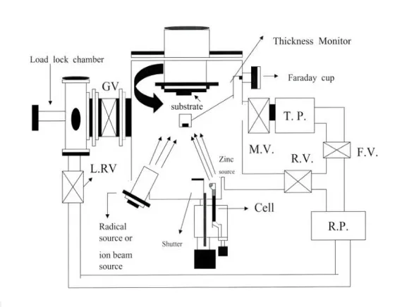
The Al-doped ZnO films were prepared by the ion-beam-assisted deposition technique on glass substrates (Corning 7059).
It consists of a focused Cold Hollow ion beam source. The main source was prepared with 10cm diameter, and 600 incident angles served as a sputtering ion beam source.
Prior to deposition, the substrates (2☓2 cm2) were cleaned during the 5 minute in acetone, ethanol and distilled water, sequentially, and dried with nitrogen gas. The doped ZnO films were deposited at room temperature by using Al-doped ZnO (2:8) Pellet materials.
Fig. 1. A Schematic diagram of the IBAD system
The chamber was evacuated to 1☓10-7 Pa. As the operating pressure was maintained to 4☓10-4 Pa, the oxygen partial pressure was controlled between 3☓10-4 and 4☓10-4 Pa by admitting oxygen gas through a leak valve. The flow rate of pure oxygen (99.99%) was set to be 10 sccm. and the substrate was fixed at 45o.
The distance between the Ion gun source and the substrates is 55cm. A Cold hallow ion beam source is used to produce oxygen ion energy. The ion beam energy changed from 0eV to 600 eV. The variable process parameters such as primary oxygen ion bombarding current and oxygen ion dose were constantly held to plasma current 300 mA and 1☓1015 ion/cm2, respectively.
The optical transmission was measured in wavelength from 200 to 800 nm with a UV-visible spectrophotometer (UV-1600PC, Shimadzu). Surface morphology of the Al-doped ZnO thin film was obtained by using Atomic Force Microscopy (SPA 300, Seiko Instrument) and the Microstructure was examined by Scanning Electron Microscopy (SEM) analysis. (S-2700, HITACHI, Japan).
The structural properties were investigated by an X-ray diffraction meter (Shimadazu XRD 6000) operated at 40 kV and 300 mA with the Cu-Kα radiation (wavelength 1.5415 Å) .The resistivity of the film was measured by a four-point-probe method (Model RT-70, NAPSON, Japan), and Hall mobility was measured by the van der Pauw method (Lake Shore 665).
B. DSSC PREPARATION
Porous TiO2 thin films were formed on Al-doped ZnO thin film glass substrates by the doctor blade coating method, and followed by annealing in air at 500℃ for 1 hour in order to remove organic additives. The TiO2 thin film layers were composed of ultrafine nano-particles of 20 nm average size. Its thickness was about 9um.
C. DEVICE ASSEMBLY
syringe. The electrolyte contained 0.6 M 1-butyl-3-methylimidazoliumiodide, 0.03 M I2, 0.5 M tert-butylpyridine, and 0.1 M guanidinium thiocyanate in acetonitrile/valeronitrile 85/15(volume) solution.
The current density-voltage (J-V) measurements were carried out under the illumination of 60 mW/cm2, respectively by using a digital source meter (McScience Co. Ltd., model-300). The simulated sunlight was provided by a 500 W Xe lamp fitted with an AM 1.5 spectrum. The active area of the DSSCs was fixed to 0.25 cm2 by a light shading mask.
Ⅲ. RESULTS AND DISCUSSION
A. PREPARATION OF AL-DOPED ZINC OXIDE FILMS DEPOSITED BY ION-BEAM-ASSISTED MOLECULAR BEAM EPITAXY (MBE).
It is well known that the structural properties of Al-doped ZnO thin film are strongly dependent on the process condition.
30 60 90
0 800 1600 2400
Co
u
n
ts
2 Theta (Degree)
(d)Ion beam 600eV
(c)Ion beam 300eV
(b) Ion beam 100eV
(a) RT
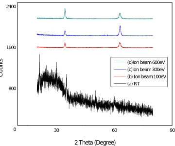
Fig. 2. XRD patterns around the (002) peak and (103) peak for Al-doped ZnO thin films deposited with changing oxygen ion energies irradiated normally on the Al-doped ZnO surface Thin film and room
Al-doped ZnO thin film deposited oxygen ion beam energy at 100eV, XRD analysis show the change of preferred orientation (002), and (103). The reason is explained by the increase of the assisted ion beam energy, so two intensities peak were appeared on the Al-doped ZnO thin film with the increase of ion beam energy. It is connected with the increase of oxygen vacancies. [12-15]. when the ion beam energy is more increased to 300 eV, it is observed that the crystal oriented is rearranged from (002) to (103) plane .This can be explained as the ion channeling effect [16-17] and anisotropic radiation effect [18].. In the case of the ion channeling effect, the direction of the ion beam energy have the highest effect on the crystal plane, but in this research, the ion channeling effect can be ignored because the substrate was rotated in the chamber when the Al-doped ZnO thin film was deposited. Instead, most of all, an important element is the Anisotropic Radiation effect. It is delivered to the ion beam energy momentum toward each crystal plane [19]. When the Al-doped ZnO thin film is deposited on the glass substrate at 300eV, The grains size is clearly increased and became denser and oxygen vacancies are increased due to the ion beam energy increase. That is to say, the oxygen ion and atom mobility can easily diffuse in the film and then it is moved in the preferentially oriented. Finally it can change the crystallinity in the Al-doped ZnO thin film.
With the ion beam energy is more increased to 600 eV, the crystal orientation is re arranged in the (002) plane than in the (103) plane by the Ion beam Radiation Damage effect
The high ion beam energy is arrived at substrate, it is caused by the deterioration of crystalizability in the Al-doped ZnO thin film by radiation damage effect, its effect is similar to Re-sputtering effect. According to the Kheyrandish et al result, they were deposited TiN thin film depending on the changes of ion beam energy.[20]
In case of the TiN thin film grown without ion irradiation, its phase was amorphous phase, While the TiN thin film irradiated at 300 eV, it showed the preferred growth in the (100) direction, and with the increased ion beam energy at 400 eV, its phase is restricted to [100]. From these results, we concluded that high ion energy have effect on thin microstructure, it can change the crystalline and disorder in preferred growth in the film.[21]
Figure 3. shows the SEM image of the AZO thin film by changing the Ion beam energy at 0 eV, 100 eV, 300 eV, and 600 eV.
Figure 3(a) shows an Al-doped ZnO thin film sample without Ion beam energy, it is showed the amorphous phase or small polycrystalline structure with the few nm grain which the particle size is almost not observed or some particles are showed very weak intensity by the X-ray diffraction analysis.
Figure 3(b) showed an Al-doped ZnO thin film sample at 100 eV, it showed the small microstructure by the relative low ion beam energy. This film has a lot of small grains and a lot of agglomerated grains. However, as the ion beam energy increased at 300eV, the average grain size gets increaser than other condition.
It means that surface ad atoms had an enough mobility to migrate on the Al-doped ZnO thin film by the Ion beam energy, and it is transferred to the kinetic energy in the microstructure. In the end, it leads to the largest particles size. This result suggest that Al-doped ZnO thin film has a higher density than other condition. 21-22) The low-energy oxygen ion beam is important and it has effect on the crystallinity in the Al-doped ZnO thin film, the primary effect of the ion bombardment is to enhance ad-atom mobility, And agreed with the results of cho in which irradiation with a lower energy oxygen ion beam results in a lower resistivity and higher mobility of the Al-doped ZnO thin film. [23]
The type of the largest particles size structure can often be observed by ion beam assisted deposition or the other method such as sputtering method. [24]
In addition, according to the literature, the large grain structure is expected to decrease the resistivity because of the large mobility.[26]
It comes a conclusion from the ion beam energy at 300eV; we were obtained an improvement of mobility, and carrier concentration. However, in this study, as the ion beam energy increases to 600 eV, the microstructure of Al-doped ZnO thin film was changed remarkably. The largest particles size structure disappear and change the small grain size due to the intense radiation damage, its primary effect is transferred to the energy , it lead to change the structure in the Al-doped ZnO thin film.
The radiation damage effect have a lot of the defect sites and it act as nucleation sites to form the small grain structure.[27]
With the ion beam energy increases to 600 eV, the small grain size has effect on the electrical property, optical property.
According to the Cho et.al Research, they claim as the ion energy increases over 500eV, The larger grain boundary scattering density, ionized impurity scattering, the neutral Defect scattering and the negatively charged oxygen scattering may affect to the
Electrical property, optical property, and it reduced ad atom mobility and created small grains, micro pore in the film by the irradiation damage [28].
The decrease of the mobility and the carrier concentration at 600eV may create the small grain, a lot of grain boundary and may contribute the free carrier trap in the Al-doped ZnO thin film. It will have a bad effect on the electrical and optical properties due to the high energy irradiation damage at higher ion energies.
Fig. 3. SEM Photographs of conventionally evaporated Al-doped ZnO films and cross section of Al-doped ZnO film on surface glass with varying oxygen ion energies: (a) 100 eV discharge (b) 300eV, (c) 600eV
In order to consider the effect of Ion beam energy on optical property, we measured optical transmittance in the 200-800nm wavelength by UV –Visible spectrometer
Figure. 4 showed the optical transmittance of the Al-doped ZnO thin film by oxygen ion beam assisted molecular deposition.
According to the experiment result, the Al-doped ZnO thin film without ion beam irradiation shows low transmittance less than 80%. A bare glass substrate is used as a reference. It cannot be used as a transparent electrode due to the amorphous phase or polycrystalline structure due to the evaporation effect. However In cases of the Al-doped ZnO thin films at the ion beam energy of 100eV and 300eV, its transmittance is changed from 80% to 86%r. especially the Al-doped ZnO thin film deposited at 300eV were obtained high transmittance over 85%
In the film, high transmittance curve lead to a steeper optical transmission curve, which indicates lower defect density near the edge and it, was a shift in the absorption edge to shorter wavelength. It is explained to the Burstein Moss shift. [29].
This result suggests that Al-doped ZnO thin film at 300 eV has a higher density than other samples. Daeil Kim et al showed a similar result. 22) However Al-doped ZnO thin film at 600 eV, transmittance is decreased about 80% by ion beam damage effect. The decrease of the light transmittance is connected with the increased optical absorption and surface scattering. [30]
200 300 400 500 600 700 800
0 20 40 60 80 100
T
ra
n
sm
it
ta
n
ce
(
n
m
)
wavelength (nm)
Ionbeam0eV Ionbeam100eV Ionbeam300eV Ionbeam600eV
The surface roughness is very important in the opto-electrical device
For organic light-emitting devices (OLED) application, transparent conductive film require the high electrical conductivity, the surface smoothness, and high optical transmittance and so on. Especially, the root mean square (RMS) has effect on the optical property and electrical property, In addition, its results showed by other deposition methods. [31]
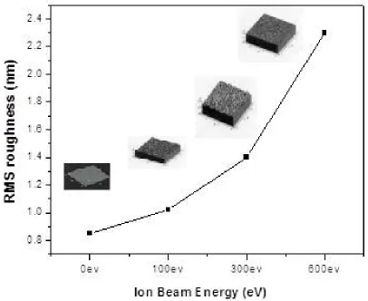
Fig 5. shows the surface morphology by the ion beam energy variation.
The root mean square (RMS) is in the range of 0.5nm- 3nm. In this experiment shows that the surface roughness is affected by Ion beam energy treatment, The experiment result show the sample without ion beam treatment, the rms value of the surface roughness exhibits relatively smooth surface with RMS of 0.7nm. However, with the assisting ion beam energy further increased up to 100 eV ,300 eV ,600 eV, the RMS of the AZO thin films is drastically increased up to about 1.1nm, 1.4nm, 2.4nm,
Fig. 5.The values of the surface roughness of the conventionally evaporated Al-doped ZnO film in oxygen ion environment and the Al-doped Zno films deposited at 0eV, 100eV, 300eV, 600eV
that the Rms value increases with increasing the ion beam energy, and it lead to increase the surface migration of ad atoms ,However high energy ion beam condition, it deteriorate the microstructure in the film. [33]
Finally the rougher surface and the rougher interface will scatter more electrons and photons in the film, it may also reduce optical property and increase electrical property. The influence of the assisting ion beam energy on the RMS is consistent with the SEM results above. In general, the resistivity of Al-doped ZnO thin film is decided by the mobility and carrier concentration, and the resistivity of Al-doped ZnO thin film is connected with the oxygen Vacancies, grain boundaries, residual stress and impurity scattering and surface roughness and so on. [34]
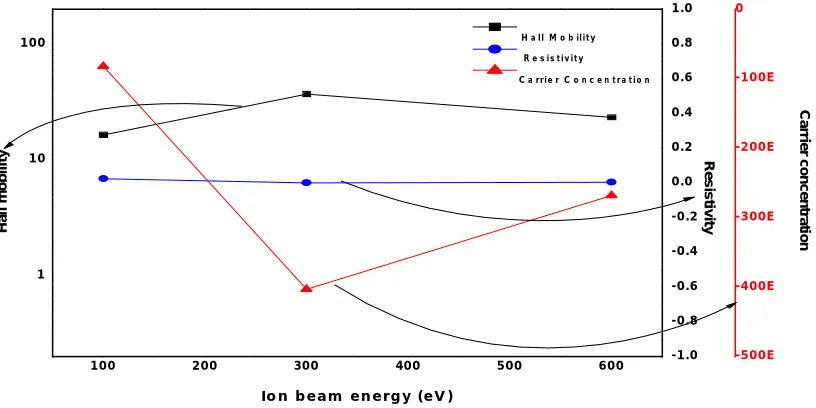
Figure 6. Showed the result of electrical resistivity property for Al-doped ZnO thin film films by changing of Ion beam energy.
The resistivity varies from 4×10⁻³Ωcm to 8.5×10⁻⁴Ωcm. As a result of experiment, A low electrical resistivity of 8.5×10⁻⁴Ωcm
obtained at 300 eV. And it is quite clear that Ion beam energy at 300 eV condition appear the best grain crystal growth. The larger grain size means a lower grain boundary scattering, low defect and low residual stress, which leads to an increase in the conductivity.
It means that low Ion beam energy plays an important role in the Al-doped ZnO thin film growth and result in a lower resistivity and a higher mobility of the Al-doped ZnO thin film
However, with the ion beam energy at 600eV, it is also observed that the conductivity decreased .This is attributed to the increase of the small grain, grain boundary, and surface roughness in the Al-doped ZnO thin film by ion beam damage effect [35].
From these results, we realized that the excessive ion energy ( >500 eV ) is not favorable due to the high ion beam energy, it lead to increase surface roughness, change the microstructure, and as a result it deteriorate the electrical properties and optical properties in the Al-doped ZnO thin film.
Finally, in case of the polycrystalline structure, the electrical property was changed significantly with grain size due to the scattering at the grain boundaries by ion beam effect.
Finally we realized that Al-doped ZnO thin films can be controlled with ion beam energy to obtain the transparent conducting oxide substrate, and Al-doped ZnO thin film must make it possible to produce in the low oxygen ion beam energy at 300 eV, in this research.
1 0 0 2 0 0 3 0 0 4 0 0 5 0 0 6 0 0 1
1 0 1 0 0
C a rri e r C o n c e n t r a t i o n R e s i s t i v i t y
H a l l M o b il i t y
C ar rier co n cen tr at io n R e s is tiv it y H a ll m o b ilit y
I o n b e a m e n e r g y ( e V )
- 1 . 0 - 0 . 8 - 0 . 6 - 0 . 4 - 0 . 2 0 . 0 0 . 2 0 . 4 0 . 6 0 . 8 1 . 0
- 5 0 0 E - 4 0 0 E - 3 0 0 E - 2 0 0 E - 1 0 0 E 0
B. RESULTS AND DISCUSSING OF TIO2 BASED SOLAR CELL
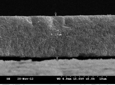
In order to comparison about solar cell efficiency, dye-sensitizes TiO2 based solar cells were fabricated on 4 kinds of Al-doped ZnO this film glass substrates. Fig 7.8 show the FE-SEM image, TiO2 Thin film are about 20nm in diameter and mesoporous shape and its thickness are about 9um. and XRD Pattern of the coated TiO2 thin film on AZO glass substrate.
Fig. 7. FE-SEM Image of the TiO2 grain size
Fig. 8. FE-SEM cross section Image of the TiO2 thin film
0 20 40 60 80 100 1000 2000 3000 4000 5000 6000 7000
TiO2 ( Antase) A(101) A(116) A(107) A(303) A(213) A(105) A(200) R(200) R(110) C o u n ts
2 Theta (Degree)
Fig 9. X-ray diffraction of pattern of TiO2 thin films annealed in O2 at 500
Fig 10. shows the J–V curves of DSSCs fabricated on Al-doped ZnO thin film glass grown at room temperature and the accelerating voltage were kept constant at 100 mA and 500eV, respectively. The screen voltage was varied from 100 eV to 600 eV.
In this study, the sample preparation conditions were the same condition, only the condition of substrate were different by changing the ion beam energy effect.
As a result of experiment, as the particles size increases in the transparent conducting oxide thin film, Solar cell energy conversion efficiency is increased by ion beam energy effect.
0.0 0.2 0.4 0.6 0.8 1 .0 -0.08 -0.07 -0.06 -0.05 -0.04 -0.03 -0.02 -0.01 0.00 0.01 0.02 P h o to c u rr e n t d e n s it y ( m A /c m 2 )
voltage (V)
R T 100 300 600
Table 1. summarizes the open circuit voltage(VOC), short circuit current density(JSC), fill factor(FF), conversion
efficiency(η), and so on, As a result from experiment, the DSSC fabricated on Al-doped ZnO thin film glass grown at room temperature, and Ion beam energy with the 300eV. exhibits higher VOC (0.727 V), JSC (12.6mA/cm2), FF
(41.2%) and η (3.8%) than that fabricated on the other Al-doped ZnO thin film glass substrate sample.
In case of the Al-doped ZnO Thin film sample with the Ion Beam energy 300eV in oxygen gen ambient gas, the grain size of the Al-doped ZnO thin film is bigger than the other samples.
It leads to a decrease in the effect number of incident photons. According to the Noh et AL’s result, he has obtained the similar results. [37]
The DSSC fabricated on the Al-doped ZnO thin film grown at room temperature by Ion beam energy 300eV exhibits superior conversion efficiency (3.8%) than the other sample
Table 1.
Sample Jsc(mAcm-2) Voc(V) FF η (%)
No-treatment 4.3 0.495 0.534 1.5%
Ion Beam 100eV 5.4 0.646 0.687 2.4%
Ion Beam 300eV 12.6 0.727 0.412 3.8%
Ion Beam 600Ev 4.2 0.535 0.51 1.2%
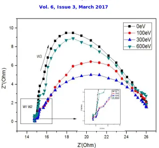
In order to investigate the effect of Grain size of Al-doped ZnO thin film by Ion beam energy effect in the DSSCs Cell, Electro chemical impedancen spectroscopy method (EIS) was used. In gerneall, EIS analysis method explain about Al-doped ZnO thin film based the photovoltaic characteristics.[38-39]
The DSSCs were assembled in different Ion beam energy ( 0eV , 100eV , 300eV , 600 eV ) under the Al-doped ZnO thin film Condition.
Fig. 11 illustrate the EIS data of the solar cells with various Ion beam energy of the Al-doped ZnO Thin films in DSSCs Samples.
The EIS Nyquist plots of DSSCs without and with Al-doped ZnO thin films containing different Ion beam energy condition. From the result of the EIS Nyquist plots, The cells were obtained three semicircles and it is associated with the the charge transfer resistance.
This information can be explained by the photovoltaic characteristics : (i) TCO and Count er electrode/ electrolyte interface (Rpt), (ii) electron transfer and recombination Kinetics at TiO2/ dye/ electrolyte Interface (Rct) and Nerst diffusion in the electrolyte.[40]
According to the result of the radius of semicircles, it is seen that the charge transfer resistance (Rpt) is lower for Al-doped ZnO Thin film at the 300 eV condition than the other cell. In addition, When ion beam energy irradiated at the 0eV ,100eV, 600eV samples see the impedance graph, The semicircle showed the results are not clear, However, When Ion beam energy irradiated sample at 300 eV condition, it can be seen that the semicircle appears relatively. It means that the charge transfer are improved by the influence of the microstructure. From the result of experiment, optimization of condition plays an important role as an in the Transparent conducting oxide layer facilitating the electron transport to the external circuit and so on. It is connected with the highest efficiencies due to the great the grain size in the Al-doped ZnO Thin film substrate.
Therefore, In order to transparent conductive glasses applying in DSSCs, it have a low sheet resistance, a high transmittance and an excellent surface microstructure and so on
Fig. 11. EIS Nyquist plot of DSSCs fabricated without and with Al-doped ZnO Thin film by different Ion beam energy.
Ⅳ. CONCLUSION
As a result of experiment, Al-doped ZnO thin film with the room temperature prepared by the irradiation a lower energy oxygen ion beam (<300Ev), shows a resistivity of 8.5×10⁻⁴Ωcm, carrier density of 5.8ⅹ1020 cm-3, optical transmittance above 85% at wavelength of 550nm, and surface roughness of 1.5nm.
The Al-doped ZnO thin film electrodes at 300 eV exhibited highly enhanced conversion efficiencies of 3.8% compared to the conventional Al-doped ZnO thin film electrode (1.5%). The great nano-structure of the Al-doped ZnO film electrode played a key role in improving the photovoltaic performance of the DSSC. The enhanced of the great particles lead to the electron diffusion and reduced the surface states. The light-harvest efficiency also increased, particularly at long wavelength region because of the enhanced light-scattering effects in the presence of great nano-grain structure.
Therefore, transparent conductive electrode applying in DSSCs must have excellent surface roughness and microstructure. As a result experiment, its condition is connected with the electrical property and optical property and so on.
REFERENCES
[1] Q. Zhao, X.Y. Xu, X.F. Song, X.Z. Zhang, D.P. Yu, C.P. Li, L. Guo, “Enhanced field emission from ZnO nanorods via thermal annealing in oxygen” Appl. Phys. Lett, vol. 88 , pp. 033102. (2006),.
[2] K. L. Chopra, S. Major and D. K. Pandya, “Transparent Conductors—A Status Review,” Thin Solid Films, Vol. 102, No. 1, pp. 1-46. (1983),. [3] C.G. Granqvist, A. Hultaker, “Transparent and conducting ITO films: new developments and applications” Thin Solid Films Vol.411, issue1, pp.
[4] Tun CJ, Sheu JK, Pong BJ, Lee ML, Lee MY, Hsieh CK. “Enhanced light output of GaN-based power LEDs with transparent Al-doped ZnO current spreading layer” IEEE Photonics Technology Letters Vol: 18, Issue: 1 pp274. (2006),.
[5] J. Hu and R. G. Gordon. “Textured aluminum-doped zinc oxide thin films from atmospheric pressure chemical-vapor deposition.” J. Appl. Phys. 71, Vol 880 (1992),.
[6 ] X.H. Zhang, S.J. Chua, A.M. Yong, and S.Y. Chow, Exciton radiative lifetime in ZnO quantum dots embedded in SiO, matrix, Appl. Phys. Lett. 88. 221903 (2006).
[7] K. Maki, N. Komiya, and A. Suzuki, “Fabrication of thin films of ITO by aerosol CVD,” Thin Solid Films, vol. 445, no. 2, pp. 224–228, (2003),.
[8] K. Miyamoto, M. Sano, H. Kato and T. Yao, “High-Electron-Mobility ZnO Epilayers grown by plasma-assisted molecular Beam Epitaxy,” Journal of Crystal Growth, Vol. 265, No. 1-2, pp. 34-40, (2004),.
[9] H. El Rhaleb, E. Benamar, M. Rami, J.P. Roger, A. Hakam, and. A. Ennaoui: “Spectroscopic ellipsometry studies of index profile of indium tin oxide films prepared by spray pyrolysis”. Appl. Surf. Sci. Vol 201, No.138 pp.12. (2002),.
[10] H. Fang, T. Miller, B.R. Rogers, R.H. Magruder III, R.A. Weller, “Effect of oxygen content on piezoresistivity of indium tin oxide thin films prepared by pulsed laser deposition,” J. Appl. Phys. 97 083502 pp.1-5. (2005)
[11] M. Gilo, R. Dahan, N. Croitoru, “ Transparent indium tin oxide films prepared by ion-assisted deposition with a sing-layer overcoat” Opt. Eng. Vol 38(6), pp953-957, (1999),.
[12] L.J. Meng, M.P. dos Santos, “Properties of Indium Tin Oxide Films Prepared by RF Reactive Magnetron Sputtering at Different Substrate Temperature” Thin Solid Films Vol pp 322, 56(1998) .
[13] L.J. Meng and F. Placido, “Annealing effect on ITO thin films prepared by microwave−enhanced dc reactive magnetron sputtering for
telecommunication applications”, Surf. Coat. Technol. 166, 44–50, 14 (2003).
[14] John L. Vossen, Thin Film Processes, Academic Press, New York, 5 ,175,. (1978)
[15] Liu, T. Matsutani, N. Yamamoto, M. Kiuchi,” High-quality indium tin oxide films prepared at room temperature by oxygen ion beam assisted deposition” EPL (Europhysics Letters), Volume 59, Issue 4, pp. 606-611 (2002).
[16] R. M. Bradley, J. M. E. Harper and D. A. Smith, “Theory of Thin Film Orientation by. Ion Bombardment during Deposition,” J. Vac. Sci. Technol. A 5, 1792 (1987).
[17]Ensinger.W., “Low enery ion assist during deposition-an effective tool for controlling thin film microstructure.” Nuclear Instruments and
Methods in Physics Research B: Beam Interactions with Materials and Atoms Vol 127/128, PP 796-808,(1997),..
[18] L.Dong, and D. J. Srolovitz, “Mechanism of texture development in ion-beam-assisted deposition", Applied Physics Vol 75(4), pp. 584-586, (1999),.
[19] W. Ensinger, “Low energy ion assist during deposition – an effective tool for controlling thin film microstructure”, Nuclear Instruments and Methods in Physics Research B 127/128, pp796–808 ,(1997),.
[20] H. Kheyrandish, J. S. Colligon, J.-K. Kim, “Journal of Vacuum Science & Technology A - J VAC SCI TECHNOL” A, vol. 12, no. 5, pp. 2723-2727, (1994),.
[21] ] K. G. Ressler, N. Sonnenberg, and M. J. Cima,” Ion Beam-Assisted Deposition of Biaxially Aligned CeO2 and ZrO2 Thin Films on Amorphous Substrates.” MRS Proceedings / Volume 316 / pp 2769-77 ,(1993),.
[22] Daeil, Kim, Steven Kim, Surface and Coating Technology. “Effect of secondary ion beamener gy and Oxygen partial pressure on the structural, morphological and optical properties of ITO films prepared by DMIBD technique”, vol 154 pp204-208 .(2008),.
[23] Hiroyuki Hirayama, Shigeru Baba, Akira Kinbara “Electron energy loss measurements of In/Si(111) superstructures: Correlation of the spectra with surface superstructures”, Applied Surface Science, Volumes 33–34, pp 193-198 ,(1988).
[24] M. Kamei, Y. Shigesato, and S. Takaki, “Origin of characteristic grain-subgrain structure of tin-doped indium oxide films,” Thin Solid Films, vol. 259, no. 1, pp 38-45, (1995),.
[25] M. Higuchi. M. Sawada and Y. Kuronuma, ““Microstructure and Electrical. Characteristics of Sputtered Indium Tin Oxide Films”, J. Electrochem. Soc, Vol 140. pp1773, (1993).
[26] . J.S. Cho, S.K. Koh, K.H. Yoon,” Material properties of indium oxide films prepared by oxygen ion assisted deposition “ J. Electrochem. Soc. Vol 147 pp1065,(2000),.
[27] R. Bel, Hadj Tahar, T. Ban, Y. Ohya, Y. Takahashi, “Tin doped indium oxide thin films: Electrical properties” Journal of Applied Physics vol
83, pp 2631 (1998)
[28] J. J. M. van der Holst, M. A. Uijttewaal, B. Ramachandhran, R. Coehoorn, P. A. Bobbert, G. A. de Wijs, and R. A. de Groot, Phys. Rev. B vol
79, pp 085203 (2009).
[29] J. I. pankove, Optical Processes in Semiconductors, (Dover Publications, N.Y,), pp. 35-42,(1971),.
[30] David C Paine, T Whitson, D Janiac, R Beresford, Cleva W. Ow-Yang, Brian Lewis,
“A study of low temperature crystallization of amorphous thin film indium–tin–oxide”, Journal of Applied Physics vol 85, 12 pp 8445-8450, (1999),. [31] H. Kim, J.S. Horwitz, G. Kushto, A. Pique´, Z.H. Kafafi, C.M. Gilmore, D.B. Chrisey, “Transparent conducting aluminum-doped zinc oxide
thin films for organic light-emitting devices”. J. Appl. Phys. Vol 88 pp 6021. (2000)
[32] K. G. Ressler, N. Sonnenberg, and M. J. Cima,” Ion Beam-Assisted Deposition of Biaxially Aligned CeO2 and ZrO2 Thin Films on Amorphous Substrates.” MRS Proceedings / Volume 316 / pp 2769-77 ,1993.
[33] L.Dong, and D. J. Srolovitz,” "Mechanism of texture development in ion-beam-assisted deposition." Applied Physics Letters 75(4):pp 584-586,(1999),.
[35] M. Kamei, Y. Shigesato, and S. Takaki, “Origin of characteristic grain-subgrain structure of tin-doped indium oxide films,” Thin Solid Films, vol. 259, no. 1, pp 38-45, (1995),.
[36] Sangwook Lee, In-Sun Cho, Ji Hae Lee, Dong Hoe Kim, Dong Wook Kim, Jin Young Kim, Hyunho Shin, Jung-Kun Lee, Hyun Suk Jung, Nam-Gyu Park, Kyungkon Kim, Min Jae Ko, Kug Sun Hong “Two-Step Sol− Gel Method-Based TiO2 Nanoparticles with Uniform Morphology and Size for Efficient Photo-Energy Conversion Devices”, Chemistry of Materials Vol 22, 6, pp 1958-1965,(2010),.
[37].J.H.Noh, S.Lee, J.Y.Kim, J.K.Lee, H.S.Han, C.M.Cho, I.S.Cho, H.S.Jung, K.S.Hong, “Nb-doped TiO2: a new compact layer material for TiO2 dye-sensitized solar cells”, J. Phys.Chem. C Vol 113, pp1083. (2009)
[38] J. Van de lagematt, N.-G. Park, A.J. Frank, “Influence of Electrical Potential Distribution, Charge Transport, and Recombination on the Photopotential and Photocurrent Conversion Efficiency of Dye-Sensitized Nanocrystalline TiO2 Solar Cells: A Study by Electrical Impedance
and Optical Modulation Techniques” J. Phys. Chem. B, , 104 (9), pp 2044–2052, (2000),.
[39] T. Hosbikawa, M. Yamada, R. Kikuch, K. Equchi, “Impedance Analysis of Internal Resistance Affecting the Photoelectrochemical Performance of Dye-Sensitized Solar Cells”J. Electrochem. Soc., 152, 68. (2005),.