80
Available online at www.ijiere.com
International Journal of Innovative and Emerging
Research in Engineering
e-ISSN: 2394 – 3343 p-ISSN: 2394 – 5494
Switching Reduction in CMOS Circuits using Multistage
Clock Network
1
Manjusha M,
1Blessy B I,
2T.Joby Titus
1UG Scholar, Department of ECE, Sri Ramakrishna Institute of Technology,Coimbatore-10 2Assistant Professor (Sr.Gr), Department of ECE, Sri Ramakrishna Institute of Technology,Coimbatore-10
ABSTRACT:
This paper gives the method to reduce switching power in the CMOS circuit using multistage clock network. Power consumption is the major problem that we face in the portable devices. In this reduction technique, we investigate the problem of high power consumption of CMOS circuits and introduced a method to reduce power, using multistage clock networks. The clock with variable phase is provided to the logic circuits. The clock phase variation is selected by lookup table controller, to reduce the unnecessary switching. The simulation of proposed technique is analyzed using tanner EDA tool. This analysis is carried out with multistage clock network and without multistage clock network. The lookup table based multistage clock controller provides better reduction in power and delay compared to previous stages.
Keywords:CMOS, Buffer, Multistage clock networks, Power, Delay.
I. INTRODUCTION
Now-a-days the main challenge for IC industries is to face power consumption during design. In many portable devices, life of battery is not prolong due to power consumption. It also requires cooling devices since heat is evolved due to high power consumption. It increases the cost of the product too.
Average power consumption in CMOS technology is the sum of dynamic power, short circuit power, leakage power and static power. Here we concentrate more on dynamic power or switching power. Power consumed while switching from one state to another is dynamic power. High dynamic power is due to complex clock network. Dynamic power consumption is reduced by applying retiming guide and supply voltage to the retiming network [4].
𝑃𝑑𝑦𝑛= 𝑘𝑐𝑓𝑉𝑑𝑑2………..(1) where k-switching activity factor
c -loading capacitance f-clock frequency Vdd-supply voltage
Dynamic power can be reduced by minimizing • switching activity factor k
• load capacitance c • clock frequency f • supply voltage Vdd
81 buffer, less jitter is generated. An ILO uses high pass and low pass filtering to suppress internal and input noise by lowering jitter at output. In ILO, a quantitative study based on circuit and micro architectural level simulation is performed [2]. The best way to decrease dynamic current in the driver net, is to reduce the transistor width when the net capacitance are not dominating [8]. Integrating optical components with bulk CMOS is a challenge. A compatible CMOS optical clock distribution and recovery system is designed with a fully feasible on-chip electronic integrator. To reduce the power dissipation, multiple clock stages are used replacing every stage with optical clocking [7].The energy-efficiency is increased by using a low power architecture called as Wallace architecture [9]. Optimization problem in checkers is reduced by increased inputs [10].
II. EXISTING METHODS
A. H-Tree clock distribution network
A distributed model of two level resonant H-tree structure is described, supporting the low power, skew and jitter design resonant H-tree clock distribution network. This demonstrates the design of two level resonant H-tree network, distributing 5-GHz clock signal in a 0.18µm CMOS methodology. This exhibits an 84% decrease in power explanation as compared to standard H-tree clock distribution. The sensitive analysis of resonant H-tree clock distribution network is also provided.
Figure 1. Global clock distribution network
To support distributed square waveform slew rate, a H-Tree sector and the clock grid for sufficient bandwidth is designed. A bandwidth of 0.5/t is required for distributing a square clock signal with a skew of t. By Fourier theorem, the time domain response is nearly equal to the ideal square signal with increased bandwidth but bandwidth depends upon rise time and output resistance of the driving buffer. The methodology depends on the transfer function of the two level H-Tree defined as a sector such that the fundamental harmonic of the input square wave is transferred to the output. The output signal behaves as sinusoidal at the leaf nodes, so to convert the sinusoidal waveform into a quasi-square wave, inverters are placed. The H-Tree sector function is used to determine the value of the on-chip spiral inductors, driving buffer resonance and capacitors that produce the minimum power consumption. The frequency of the clock signal exceeds multi gigahertz. Hence to incorporate high frequency effects into the system behavior, distributed models are interconnected. This method uses classical distributed model, where an incremental section of line length is modeled as lumped element circuit. For a ±25% change in spiral wire width, the output voltage is less than ±1% and the power consumption is between ±2%. This shows the high tolerance of H-Tree with respect to variations in the on-chip spiral inductor. Here on the increase of spiral inductor wire width increases the inductance, saving additional energy. The resistance of wire is inversely proportional to the cross-sectional area of the wire. Increase in the interconnection width decrease the resistance thereby resulting in lower wire loss and decreasing the power dissipation.
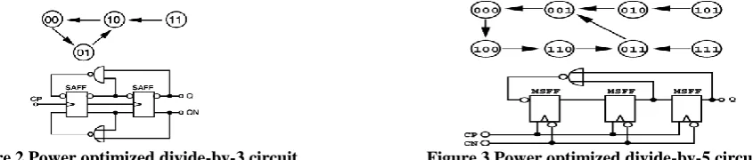
B. Power optimized high speed CMOS frequency dividers
The power optimized design of high speed CMOS logic based frequency dividers is sensitive to partitioning and selection of FF type and logic family. The power consumption of a divide-15 circuit running at 5.5GHz can be minimized by an appropriate partitioning of circuit and a careful selection of the registers. A straight forward counter-based approach would require four registers and a considerable amount of logic.
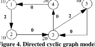
Figure 2.Power optimized divide-by-3 circuit Figure 3.Power optimized divide-by-5 circuit
81 quite high for only two flip-flops. Edge triggered flip-flops are not applicable for very high clock frequencies, as the data-to-q delay must be less than half the input clock period minus some picoseconds taking clock jitter and duty cycle distortion into account. The main intension is to divide the input frequency by a factor of two to provide highly accurate phase skew of 900.Pulse generator is partitioned into two stages. Two differential sense amplifiers are connected with pre-charged internal nodes. The operation of pulse generator is not that of latch or flip-flop based approaches. The node capacitances of the internal storage node are critical for the speed of sense amplifiers. These signals are used for coupling since the whole pulse generator is considered as an optimized full custom macro cell. The pulse generator is decoupled from the second divider stage by using inverters. Due to the variations of and/or parameter for high frequencies, the inverted output pulse signal may not reach full Vdd level and their pulse width may vary. Dynamic level converters are used to interface the pulse generator and subsequent circuit blocks to avoid cross current and enable reliable signal conditioning. The level converters in the second stage are made insensitive to the input level by the dynamic approach. This does not affect the accuracy of 900 phase skew as the circuit is absolutely symmetric. The circuit should be emphasized that the divider is dedicated for a frequency range from dc to 10GHz with rail-to-rail signal. This shows that the divider does not depend of low swing input signal or operation only in the surrounding area of the resonant frequency. Hence sense amplifiers are designed for a fast reliable decision that minimizes the switching time during which cross currents occur, that is, reduced power consumption for low frequency. The dynamic push-pull technique is sort of self-synchronized and avoids glitches completely. To strengthen noise immunity, the output inverter can be implemented with a slight hysteresis. Single ended divider structure of prior-art approaches is a main drawback if skew less complimentary output signals are required. Power supply noise causes jitter and also causes clock uncertainty. Since the divider operates with rail-to-rail signals, a large signal analysis is required for noise analysis. The controlled voltage in series to the power supply voltage is responsible for the noise in the device. The process variation and supply noise do not degrade the signal quality. Hence the divider is well suited for all wireless applications.
C. Retiming and supply voltage scaling
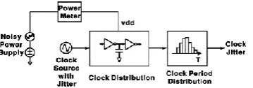
In sequential circuit design, the computational elements with high switching activity may switch many times during the clock period. The register switches only at the commencement of the clock signal. Hence in sequential circuit designing, registers are placed at the output of computational elements as to reduce dynamic power.Multiple supply voltages are used to reduce power consumption. Dynamic power consumption also can be reduced by fixed-phase retiming. Two latches replace each edge-triggered flip flop thus transforming into a two phase level clock circuit. Using this circuit one phase latch are fixed while the other phase latch are moved towards wires with capacitance and high switching activity. From the dynamic power equation the supply voltage scaling of computational element reduces the dynamic power. Scaling supply voltage of an element increases its execution delay. Minimization of dynamic power consumption (MDPC) is a problem which has been widely found in the case of digital circuits. To maximize the number of computation elements the registers should be moved from their positions, which leads to less dynamic power consumption. Moving registers from their position is achieved by basic retiming. By using the above approaches MDPC cannot be done easily generally by polynomial time algorithm. This could be overcome by using mixed integer linear program. In this synchronous sequential digital designs are represented by a directed cyclic graph with set of computational elements and set of edges.
Figure 4. Directed cyclic graph model
On the left of each node is a label which specifies the execution delay of each computational element of the circuit. Since the combinational digital design does not have wire, it can be modified into an acyclic graph. The design is assumed to be operated at a clock period which is determined by applying a retiming for clock period minimization or given by the designer. The number of supply voltage and their values are assumed to be known.
D.Multistage clock network
The problem of power minimization of rotary clock designs. A software tool is developed based on the method of partial element equivalent circuit that is able to extract SPICE netlist from layout specification of a rotary clock design. Based on the result power minimization algorithm is proposed. It has proved that for frequency ranging from 0.5 to 5GHz, rotary clock design can achieve power saving up to 80% when compared to clock tree.
82 A double loop made of interconnection is called rotary ring. Every location along the ring provides a square wave clock signal. By attaching the clock inputs to the interconnection, the registers can be connected to the rotary ring. To compensate the energy loss due to resistivity of interconnections, inverted pairs connected back to back, ie, bistable inverters are connected to the clock ring so that the clock wave can be sustained indefinitely. Multiple rotary rings are connected to form rotary array. The rings synchronize themselves at single frequency because the clock phases of different rings are locked at the merge points. Here the number of inverter pairs per rotary ring is fixed. Moreover, all the inverters are the same and distributed evenly along their corresponding rotary rings. The main objection made is that both the rotary array and rotary rings are in square shape. Therefore its dimensions can be represented by using the width of the ring or array. The clock loads to all the rings are distributed evenly. Once the rotary clock design is partitioned into multiple segments, its equivalent circuit is then extracted. In rotary clock design, when the two filaments are perpendicular to each other, their mutual inductances are often negligible and therefore said to zero. When they are parallel, mutual inductance values are calculated using formula. The rotary clock is designed using PEEC based extraction tool and PSPICE simulation. The drawback is to how drive the circuit using clock signal with a full spectrum skew. Another method used is deskewable clock distribution methodology. Here is a novel technology to distribute a clock signal from a central location to several sites on a VLSI IC. Buffered H-tree and circuitry to dynamically remove any skew that may result due to intra-die process variations are used. Only one phase detector is used. The resolution of the phase detector is inconsequential. It can be applied dynamically, either at boot time or periodically during the operation of IC.
Only one phase detector is required in a novel skew reduction technique placed at the source node of the clock tree. In this technique, the dynamic skew can be approximately zero. Here, a clock signal is driven to n points using n separate wires equally sized. Clock reliability distribution becomes harder with the increasing die size. The reference signal is distributed along the clock core such that its skew is very low. The worst case of skew comes when the skew of the reference clock signal is guard-band of the phase detectors. To reduce this, a single phase detector is used. Due to this, the return path has the same electrical environment as the forward path. By routing the return path alongside the forward path, this can be obtained. When the dies are growing larger, current VLSI ICs are buffered. The addition of buffer worsens the skew problem. The main drawback with buffering is the process and temperature variations at each of the inverters introduce skew at the leaves of the H-Tree. Phase detector consists of simple latch using two cross-coupled inverters and devices as shown.
Figure 6. Schematic of the phase detector
This also adds a capacitance at the leaf to ensure that the clock signal at each leaf has the same phase. This method deskew clock signal upto 300ps of initial skew to 3ps. Here the power consumption is 24.7% lower than the unbuffered H-Tree.
E.Low power clock distribution scheme for high performance
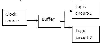
Injection-locked clocking (ILC) is used to combat deteriorating clock skew and jitter and reduce power consumption in high performance device. In the new clocking scheme, injection-locked oscillators are used as local receivers. ILC is fully compatible with conventional clock distribution network. In a standard 0.18µm CMOS technology, a test chip distributing 5GHz clock is implemented and achieved good jitter performance and a deskew range upto 80ps.
Figure 7. Circuit-level jitter simulation setup
83 mismatch is reduced, skew is reduced. It has a phase tuning capability that is the difference between input and output signals can be tuned by adjusting its free running frequency. Hence ILOs serves as a deskew buffer.
III. PROPOSED WORK
The power consumption is considerably high in the above mentioned methods. This can be overcome by using the circuit that consisting of a multistage clock network. The block diagram of the clock network is as shown in the figure 8.
Figure 8. Block diagram
The main blocks of our design are: Clock source
Buffer Logic circuits
The clock signal of particular frequency is provided as the output of the clock source. This output is given as the input to the buffer, the second block. The main function of the buffer is temporary storing. Buffer is mainly used to separate the input and the output with the same voltage. The main reason why buffer is used because, it has high impedance. Due to this impedance the buffer draws only a little amount of current. When current is decreased the power consumption is also decreased by ohm’s law. This passes the clock signal from the clock source to the two logic circuits –logic circuit 1 and logic circuit 2.
Figure 9. Circuit Diagram.
Let us consider the Lookup table function f=A+BC
Data Input Look up Table Enable output (f)
A B C
0 0 0 0
0 0 1 0
0 1 0 0
0 1 1 1
1 0 0 1
The above table shows the variation of the output for various values of A, B and C. According to the above function the output is always high whenever the value of A is high or when both the values of B and C are high.
84
Figure 10. Block Diagram of proposed technology
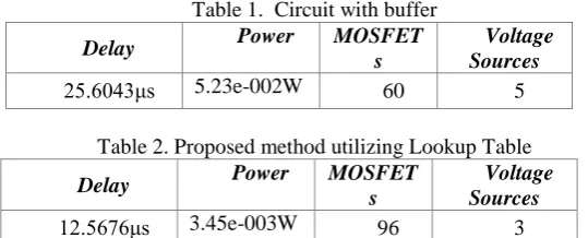
VI.COMPARISONANDRESULT
Comparing the circuit with buffered clocking network and the proposed method utilizing Lookup table, the power and delay reduction of nearly 4.985e-002W and 13.0367µs is obtained respectively.
Table 1. Circuit with buffer
Delay Power MOSFET
s
Voltage Sources
25.6043μs 5.23e-002W 60 5
Table 2. Proposed method utilizing Lookup Table
Delay Power MOSFET
s
Voltage Sources
12.5676μs 3.45e-003W 96 3
From the above tables, it is understood that the power consumption is considerably less and the delay is reduced in the proposed method than the circuit without buffer.
VII.CONCLUSION
The simulation result of the two circuits is compared. The power of the circuit with multistage clock networks is found to be comparatively less than the circuit without multistage clock network. By using this method of power reduction, power consumption in portable devices can be reduced thereby increasing the lifetime.
ACKNOWLEDGEMENT
We would like to thank our project guide Prof T. JOBY TITUS, who believed in us and spend his valuable time by providing us all the help and motivation that we needed, to successfully complete the paper.
REFERENCES
[1] Zhengtao Yu and Xun Liu, Member, IEEE, “Low-Power Rotary Clock Array Design”, IEEE TRANSACTIONS ON VERY LARGE SCALE INTEGRATION (VLSI) SYSTEMS, VOL. 15, NO. 1, JANUARY 2007, pp. 5-12. [2] Lin Zhang, Aaron Carpenter, Berkehan Ciftcioglu, Alok Garg, Michael Huang, and Hui Wu, “Injection-Locked
Clocking: A Low-Power Clock Distribution Scheme for High-Performance Microprocessors”, IEEE TRANSACTIONS ON VERY LARGE SCALE INTEGRATION (VLSI) SYSTEMS, VOL. 16, NO. 9, SEPTEMBER 2008, pp. 1251-1256.
[3] Jonathan Rosenfeld and Eby G. Friedman, Fellow, IEEE, “Design Methodology for Global Resonant H-Tree Clock Distribution Networks”, IEEE TRANSACTIONS ON VERY LARGE SCALE INTEGRATION (VLSI) SYSTEMS, VOL. 15, NO. 2, FEBRUARY 2007, pp. 135-148.
[4] Noureddine Chabini and Wayne Wolf, Fellow,IEEE, “Reducing Dynamic Power Consumption in Synchronous Sequential Digital Designs Using Retiming and Supply Voltage Scaling”, IEEE TRANSACTIONS ON VERY LARGE SCALE INTEGRATION (VLSI) SYSTEMS, VOL. 12, NO. 6, JUNE 2004, pp. 573-589.
[5] Arjun Kapoor, Nikhil Jayakumar, and Sunil P. Khatri, “Dynamically De-Skewable Clock Distribution Methodology”, IEEE TRANSACTIONS ON VERY LARGE SCALE INTEGRATION (VLSI) SYSTEMS, VOL. 16, NO. 9, SEPTEMBER 2008, pp. 1220-1229.
85 [7] Charles Thangaraj, Student Member, IEEE, Robert Pownall, Student Member, IEEE, Phil Nikkel, Guangwei
Yuan, Student Member, IEEE, Kevin L. Lear, Member, IEEE, and Tom Chen, Senior Member, IEEE, “Fully CMOS-Compatible On-Chip Optical Clock Distribution and Recovery”, IEEE TRANSACTIONS ON VERY LARGE SCALE INTEGRATION (VLSI) SYSTEMS, VOL. 12, NO. 11, OCTOBER 2010, pp. 1-14.
[8] Jordan INNOCENTI, Loic WELTER, Franck JULIEN, Laurent LOPEZ, Jacques SONZOGNI,Stephan NIEL, Arnaud REGNIER, Emmanuel PAIRE, Karen LABORY, Eric DENIS ST Microelectronics Rousset 190 av Celestin Coq, ZI – Rousset-Peynier 13106 Rousset CEDEX, France, Jean-Michel PORTAL IM2NP-UMR CNRS 6242 / Université d’Aix-MarseilleIMT Technopôle Château-Gombert 13013 Marseille, France Pascal MASSON EPOC / Université de Nice Sophia-Antipolis 1645 route des Lucioles 06410 BIOT, France,''Dynamic Power Reduction through Process and Design Optimizations on CMOS 80 nm Non-Volatile Memories Technology'', 978-1-4799-4132-2/14/$31.00 ©2014 IEEE, pp. 897-900.
[9] Flavio Carbognani,Felix Buergi, Norvert Felber, Hubert Kaeslin, Member, IEEE, and Wolfgang Fichtner, Fellow, IEEE, “Transmission Gates Combined With Level-Restoring CMOS Gates Reduce Glitches in Low-Power Low-Frequency Multipliers”, IEEE TRANSACTIONS ON VERY LARGE SCALE INTEGRATION (VLSI) SYSTEMS, VOL. 16, NO. 7, JULY 2008, pp. 830-836.