University of New Orleans University of New Orleans
ScholarWorks@UNO
ScholarWorks@UNO
University of New Orleans Theses and
Dissertations Dissertations and Theses
5-15-2009
In-situ Scanning Electron Microscopy for Electron-beam
In-situ Scanning Electron Microscopy for Electron-beam
Lithography and In-situ One Dimensional Nano Materials
Lithography and In-situ One Dimensional Nano Materials
Characterization
Characterization
Renhai Long
University of New Orleans
Follow this and additional works at: https://scholarworks.uno.edu/td
Recommended Citation Recommended Citation
Long, Renhai, "In-situ Scanning Electron Microscopy for Electron-beam Lithography and In-situ One Dimensional Nano Materials Characterization" (2009). University of New Orleans Theses and Dissertations. 966.
https://scholarworks.uno.edu/td/966
This Thesis is protected by copyright and/or related rights. It has been brought to you by ScholarWorks@UNO with permission from the rights-holder(s). You are free to use this Thesis in any way that is permitted by the copyright and related rights legislation that applies to your use. For other uses you need to obtain permission from the rights-holder(s) directly, unless additional rights are indicated by a Creative Commons license in the record and/or on the work itself.
In-situ Scanning Electron Microscopy for Electron-beam Lithography and In-situ One Dimensional Nano Materials Characterization
A Thesis
Submitted to the Graduate Faculty of the University of New Orleans in partial fulfillment of the requirements for the degree of
Master of Science in
Applied Physics
by
Renhai Long
B.S. Sichuan University, 2006
ii
Acknowledgement
This work was supported by the NSF Grant No. NSF-0403673, DARPA Grant
No.HR0011-07-1-0032, and research grants from Louisiana Board of Regents Contract
Nos. LEQSF(2007-12)-ENH-PKSFI-PRS-04 and LEQSF(2008-11)-RD-B-10.
I would like to express my gratitude to my advisor Dr. Weilie Zhou, who gave me
the opportunity to study and research at UNO. I feel grateful for the discussion with Drs.
John B. Wiley, Kevin Stokes, Leszek Malkinski and Leonard Spinu in AMRI meetings.
Thanks are also given to Dr. Zhonglin Wang who cleared much of my confusion with the
piezoelectric properties of the ZnO nanowire at 2009 AMRI-DAPAR Annual Review.
Speical thanks are given to Mr. Jiajun Chen, who trained me on all the facilities
and help me a lot during my graduate study. Kai Wang, Yuan Yao and Jinhee Lim were
very nice to prepare many high quality nanomaterials for my research. Research ideas
and attitudes learned from Drs. Zhongming Zeng, Ying Li, Zengxing Zhang, Baobao Cao
and Kun Yao are such great assets to me.
Finally, I extend my thanks to the faculty and the staff at both AMRI and the
iii
Table of Contents
List of Figures ... iv
Abstract ... vi
Introduction ... 1
Chapter 1 Introduction to
in-situ
SEM ... 2
Chapter 2
In-situ
EBL for nano device fabrication ... 5
2.1 Overview of electron beam lithography ... 5
2.2 Electron beam lithography system at AMRI ... 7
2.3 Challenge for suspended nano-structure fabrication using nano materials ... 9
2.4 Experimental details of in-situ EBL ... 12
2.4.1 Voltage-contrast imaging for EBL... 16
2.4.2 Layout editing for positioning accuracy optimization ... 18
2.4.3 Proximity effect ... 19
2.5 Results and discussion ... 20
Chapter 3
In-situ
measurements for one dimensional nano materials
characterization ... 26
3.1 In-situ SEM technology for nano-material characterization ... 26
3.2 Tools for in-situ SEM nano-material characterization at AMRI ... 27
3.3 Experimental ... 27
3.3.1 Tip preparation ... 28
3.3.2 Contact preparation ... 28
3.3.3 Manipulation of objects ... 31
3.3.4 In-situ gripping and characterization of the cross-section resistance of one-dimensional nano materials ... 32
3.3.5 Contact effect study of single ZnO nanowire using in-situ electrical characterization ... 34
Chapter 4 Conclusion ... 44
References ... 45
iv
List of Figures
Figure 1 Component graph of electron beam lithography system at AMRI. ... 7
Figure 2 LEO 1530VP SEM and NPGS PC. ... 7
Figure 3 PCI516 board of the NPGS at AMRI. ... 7
Figure 4 Beam blanker controller. ... 8
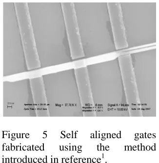
Figure 5 Self aligned gates fabricated using the method introduced in reference1. ... 9
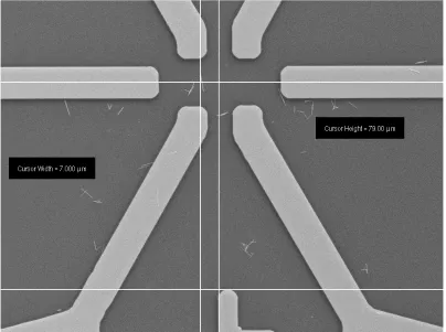
Figure 6 Measurement of the locations of the nanowire with respect to the alignment mark. ... 10
Figure 7 A schematic drawing of the fabrication process of a two-way switch. (a) Starting from an n-type silicon substrate with 600 nm thermal SiO2. (b) Fabrication of big electrodes (200nm thick) using photolithography. (c) The first layer of photoresist (200nm thick) by spin-coating. (d) Dispersed nanowires on the photoresist. (e) A second layer of photoresist to sandwich the nanowires by spin-coating. (f) In-situ wrote and developed the pattern, and windows in photoresist are showed for metallization. (g) Deposited metal into the open windows; (h) the fabricated suspended nanoswitch after lift-off process. ... 12
Figure 8 Clear voltage contrast image of a ZnO nanowire sandwiched between two layers of PMMA. The actual field area of this image is 27.057 µm by 20.293 µm, the scanning time is 190 ms, and the scale bar is 1 µm. ... 14
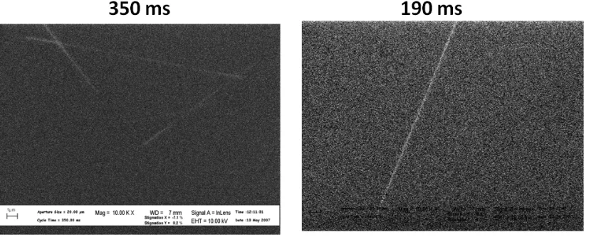
Figure 9 Contrast difference of the images captured with scan time of 350 ms and 190 ms. ... 17
Figure 10 Small balls formed on the lower left corner due to the beam dumping, which cannot be avoided in our system. ... 18
Figure 11 Two electrodes overlapped due to proximity effect. ... 19
Figure 12 (a) SEM image of a one-way ZnO nanowire nanoswitch (the scale bar is 200nm). (b) I-V curve of the nanoswitch. (c) R-V curve of the switch. ... 21
Figure 13(a) SEM image of a one-way Ni nanowire switch (the scale bar is 300nm). (b) I-V curve of the nanoswitch. ... 22
v
Figure 15 (a) SEM image of a ZnO nanowire field emission structure (the scale bar is 1
µm). (b) Field emission test result of the structure. ... 25
Figure 16 Kleindiek MM3A –EM mircromanipulator ... 26
Figure 17 Kleindiek MM3A–EM mircromanipulator controller. ... 27
Figure 18 I-V characterization of CuO2 substrate. ... 28
Figure 19 Contact improvement for in-situ electrical characterization. ... 29
Figure 20 Almost linear I-V curve achieved after contact optimization. ... 30
Figure 21 Gripping single ZnO nanowire using two manipulators ... 31
Figure 22 I-V characterization of the ZnO nanowire cross section resistance. ... 32
Figure 23 Schematic draw of the probe tip placed on the underside of a ZnO nanowire grown on the aluminum thin foil. ... 34
Figure 24 I-V characterization of a deformed ZnO nanowire with the contact on the underside. The rectify ratio was decreasing from (a) to (c) when the bending was being reduced. ... 36
Figure 25 I-V characterization of a deformed ZnO nanowire with the contact on the underside. The rectifying ratio (f) changes are small from (a) to (d) when the bending was being increased. ... 38
Figure 26 (a) The current dropped as the bending increased. (b)The current recover as the bending was released. ... 39
Figure 27 Contact placed on the compressed side of the deformed ZnO nanowire. ... 40
vi
Abstract
In this thesis, we demonstrate in-situ scanning electron microscopy techniques for
both electron beam lithography (EBL) and in-situ one dimensional nano materials
electrical characterization. A precise voltage contrast image positioning for in-situ EBL
to integrate nanowires into suspended structures for nanoswitch fabrication has been
developed. The in-situ EBL eliminates the stage movement error and field stitching error
by preventing any movements of the stage during the nanolithography process; hence, a
high precision laser stage and alignment marks on the substrate are not needed, which
simplifies the traditional EBL process. The ZnO piezoelectronics is also studied using
nano-manipulators in scanning electron microscope. Methods to improve the contact
have been demonstrated and the contacts between probe tips and the nanowires are found
to have significant impact on the measurement results.
Keywords: electron beam lithography, voltage contrast imaging, piezoelectronics,
1
Introduction
Electron microscopes are pivotal figures in the nano science and technology
research. Since the date of their birth, the potential to study the dynamic process has been
realized. A series of high resolution images actually can keep track of the gradual
changes caused by deliberate actions. Over the years, in-situ electron microscopy has
been developing fast with the thriving microelectronics industry, as more tools can be
elegantly designed and micro-fabricated. The in-situ technology is being applied to both
the existing research problems and new frontier of nano sciences.
In this work, we demonstrate the in-situ scanning electron microscope (SEM)
techniques for both electron beam lithography (EBL) and in-situ one dimensional nano
materials measurement. The chapters are organized as follows: Chapter 1 presents the
overview of existing in-situ SEM tools and applications. Chapter 2 focus on the
development of in-situ EBL through the fabrication of nanowire switches (One paper2 on
this work has been submitted for publication). Then, in Chapter 3, we describe how to do
the in-situ SEM measurement on nanowires and study the ZnO piezoelectronics using
nanomanipulators (This work3 is under preparation for submission). Finally, in Chapter 4,
2
Chapter 1 Introduction to in-situ SEM
Researchers have long realized the potentials of the microscopes to study the
dynamic process. Experiments where the specimens are acted on while they remain under
continuous observation are in-situ. Generally in an in-situ experiment, specimens are
modified in a deliberate way and the results are studied using the imaging and other
analytical tools simultaneously.
In-situ technology in electron microscopy has been developing rapidly in recent
years. Transmission electron microscopes (TEM) can now be armed with
compactly-designed components for nanoindentation 4-7, straining and tensile tests 8-20, electrical
characterization21,22 and magnetic measurements23,24 with the routine real time imaging.
Specimen environment can be changed with heating and cooling, gas and liquid injection,
materials deposition, etc.
As scanning electron microscope (SEM) is another important tool in the electron
microscope lineup, the in-situ techniques are inspirational as well. The SEM specimen
chamber is usually large enough to integrate lots of analytical tools, which are always
challenging for TEM. Besides composition, morphology and structures, the magnetic,
electrical and mechanical properties are also vital for application researches of nano
materials, which is found to be marketable by some nano-positioning companies like
Zyvex (http://www.zyvex.com), Nanotechnik (http://www.nanotechnik.com), 3rdTech
SEM can have versatile capabilities such as nanomanipulation, electron beam lithography
3
The most common tools for in-situ SEM is the piezoelectric driven
micromanipulators. Sharp probe tips with point radius down to tens of nanometers can be
installed to the arms of the manipulators for sample manipulation and electrical probing.
Many experiments can be carried out in-situ. For instance, by applying ac fields through
the probe, excitation of nanowire resonance has been achieved and observed in SEM at
real time25. However, for low level measurement special setup for noise shielding is
essential as the electron beam and the manipulators themselves are major sources of the
noise. Four-point probing is commonly carried out for low resistance measurement,
where better manipulation skills or specific four-point measurement probe are required.
While loaded with force sensor, the micromanipulators are able to perform tensile
and bending tests and monitor the response of the materials at the same time with high
quality SEM imaging, which is a favorable technique for nano electromechanical system
(NEMS) research and development. As microinjection tools are also available, tests of
materials gas and bio sensing properties can also be realized in-situ. Even magnetic
property testing26 is possible with some calibrated homemade magnets inserted into the
SEM chamber. Those in-situ SEM tool makers also discover potential market in electron
beam lithography (EBL) by offering piezoelectric-driven, stable and precise stage as a
competitive alternative to the high-end laser stages for dedicated EBL systems.
Though the in-situ SEM has a long history, a large body of in-situ SEM work is
mechanical property related: fracture toughness and fatigue measurement 27-29, tensile
deformation 30-35 and electromechanical study 31,36-38. Such kind of experiments usually
consists of an actuator for material deformation and load sensor for force read-out.
4
deformation and failure with very high resolution, while the load sensors are
simultaneously measuring the applied load electronically with relatively high resolution.
The specimen temperature can be controlled through the sample stage as well. Electrical
probes will be used if electrical characterizations are needed. Such testing systems are an
integration of electromechanical and thermomechanical components based on MEMS
technology.
Huge variety of experiments has been made possible using in-situ SEM
technology, given the convenience of integrating the required tools into the big SEM
chamber. However the output data collected in in-situ experiments are more likely mixed
with the artifacts than those ex-situ experiments. In the limited space of the chamber
filled with various scientific instruments, signals are easily distorted with unknown noises.
The recognition and elimination of artifacts should be given enough efforts both in the
development of in-situ experiment tools and in the experiment methods.
Such an introduction to applications and tools of in-situ SEM is far from
comprehensive and complete, as researchers are developing their ideas to make the
existing tools more versatile and productive. Some disadvantages of the in-situ SEM
today may be ingeniously solved tomorrow. The next chapter is a new capability we
developed for in-situ electron microscopy. We use the in-situ SEM voltage contrast
5
Chapter 2 In-situ EBL for nano device fabrication
2.1 Overview of electron beam lithography
In microelectronic fabrication, dedicated electron beam lithography (EBL)
systems can be used to either fabricate mask or directly write patterns on the wafer. Most
direct write systems use a small electron beam spot that is moved with respect to the
wafer to expose the pattern one pixel at a time. The systems can be classified as raster
scan or vector scan with either fixed or variable beam geometries. All EBL systems need
an electron source with high-intensity, high uniformity, small spot size, good stability and
a long life. Electrons can be excited from cathode of the gun by heating the cathode
(thermionic emission), applying a large electric field (field emission), a combination of
the two (thermal field emission), or even with light (photoemission)39. As the pattern is
transferred to the wafer sequentially one pixel at a time, the throughput is a major
concern of EBL, especially when a raster scan system actually requires the beam to
access each pixel. However, it is quite straightforward to use EBL to modify pattern and
produce a small quantity of test units, since no mask making process is needed. The
capability to make pattern at high resolution makes EBL an attractive technique for
research and advanced prototyping, where throughput is not a major concern. By
converting a scanning electron microscope, which has a very good electron source, a high
resolution EBL system can be made at a small fraction of cost of a dedicated system.
Of the many custom designed SEM conversions, most use a set of
digital-to-analog converters (DACs) to drive the scan coils of the microscope. The beam is
modulated with a beam blanker. Alternatively, the beam can be blanked magnetically by
6
additional problem of artifacts from the settling of scan coils and exposure at beam dump
sites. Large patterns need to be split into multiple fields for writing, and the
sub-fields are then stitched together as the stage is moved over from field to field. Being
designed for flexible imaging applications, SEM stages are neither flat nor
homogeneously in focus during writing, and even when equipped with stepper motor
control they are no more accurate than ~1 to 5 um40. Expensive high precision
laser-controlled stage is available, but this is not a favorable option of many small research labs
with tight budgets. Periodic alignment marks can be used to stitch fields accurately, but
this requires extra processing as well as the use of photolithography for fabricating
alignment marks. In order to make the alignment in a converted system as good as that of
the dedicated one, the alignment mark should be at the center of the writing field due to
large image distortion at the edge.
In summary, the inexpensive SEM EBL can provide adequate results for a
number of applications like small number of transistors, small masks, test of resists,
junctions, etc. Its practical applications are limited by stitching, alignment and
automation. Due to the difficulties with stitching, SEM EBL is not practical for device
integration over many fields. Multi-layer fabrication is challenging since much efforts
7
Figure 1 Component graph of electron beam lithography system at AMRI.
2.2 Electron beam lithography system at AMRI
The EBL at AMRI is
performed by a Carl Zeiss LEO
1530VP SEM integrated with the
nanometer pattern generation system
(NPGS version: 9.0 SEM conversion
kit sold by J.C. Nabity Lithography
Systems). Figure 1 is the component
graph of the whole system, and
figure 2 is the real image of the
whole system with the SEM on the
left and NPGS PC on the right.
NPGS is built on a Windows
PC with a PCI516 board (figure 3),
which is used to generate the X and
Y beam deflections and to provide
the signals for blanking control in a
Raith beam blanker controller (figure
4). The layout is designed using
DesignCAD and converted to runfile
by NPGS. To provide lower doses at
reasonable currents, the Nabity
8
using Faraday cup on stage and a Keithley 6485 picoammeter, and adjust the dose during
writing in case of an unstable beam. NPGS can control motorized stages, providing fully
automated sample movement and pattern alignment.
Mark alignment on the NPGS is performed by
calculating the correlation between the measured
mark image and the user-defined mark pattern.
Signal processing such as averaging and edge
enhancement can be executed before the alignment
correlation, allowing the use of low contrast or
rough marks. If the user supplies precisely defined
marks (usually printed with a mask made on a
commercial mask making tool) then NPGS can be used to correct for global rotation,
scaling, and nonorthogonality40. Typical alignment accuracies range from 1:1,000 of the
writing field to ~1:5,000, with accuracies down to ~20 nm being possible41.
9
2.3 Challenge for suspended nano-structure fabrication using nano materials
One-dimensional (1D) nanomaterials, such as nanowires, nanorods, and
nanotubes, have been extensively studied for their applications in resonator42,43, sensors
and integrated circuits44, etc. Lots of efforts have been put on the invention of standalone
application-specific nanodevices45, while some of others have been focused on the large
scale integration of nanomaterials with traditional micro-electro-mechanical system
(MEMS)46. In nanoelectromechanical system (NEMS), most structures require 1D
nanomaterials move freely on a substrate, where a suspended structure is needed47. The
most common way to fabricate a suspended nanowire structure is to etch away a
sacrificial layer beneath the nanowire. In addition, the patterned electrodes must be
precisely fabricated in a close proximity to achieve
suspended nanomaterials structures. In the case of
nanoswitches, it is necessary to fabricate a narrow
gap to achieve controlled movements of suspended
nanowires under electrical fields. A self-aligned
split gate method had been developed to fabricate
nano-size-spacing self-aligned side gates1; however,
the spacing can hardly be controlled by changing the process parameters and the
deposition materials of the electrodes for the sake of the yield. As shown in the figure 5,
the self-align gate method was used to fabricate nano gap between electrode and the
nanowire, however, only the right gaps got completely lift-off. The middle and the left
electrodes still have some metals left in the bottom gaps. Moreover, the spacings between
the electrodes and the nanowire are not identical even though they are made in the same
batch.
10
Integrating nano materials into suspended device structures was not an easy job
due to poor alignment. Accurate alignment requires the fabrication of marks using
photolithography and placing the mark at the center of the writing field, which sets lots of
restrictions on the fabrication of nano devices using nano materials. Besides, the locations
of the nanomaterials relative to the alignment mark need to be measured (figure 6) and
registered before coating the photoresist for EBL. In figure 6, the target nanowire is
measured to be located at (-7µm, 79µm) with respect to the alignment mark below. The
nanomaterials on the substrates were most likely to move during the spin coating of
11
nanomaterials are far away from the alignment mark, there would be no chance to pattern
accurately as the stage movement error had well exceeded the tolerance level of a pattern.
To tackle the problems as mentioned above, the in-situ EBL using one step
process assisted by electron voltage-contrast imaging technique was developed for
fabrication of electromechanical nanoswitches by suspending the nanowires and placing
electrodes within controllable distance. The traditional EBL requires alignment to the
alignment mark, which is not appropriate for the integration of nano materials into device
structure fabrication. The in-situ EBL we developed aligns the pattern to the target
nanomaterials, which is innovative in device fabrication process and application of in-situ
electron microscopy. Such a technique can also be applied to integrate other suspended
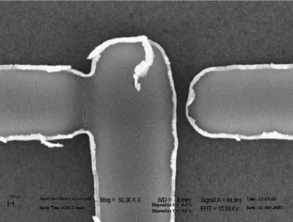
12 2.4 Experimental details of in-situ EBL
The fabrication of the nanoswitches started from the n-type silicon wafer with 600
nm thick SiO2 thermally grown on the top as shown in figure 7 (a). Big electrodes (figure
7 (b)) of 200 nm thickness were first fabricated by photolithography and metallic
Figure 7 A schematic drawing of the fabrication process of a two-way switch. (a) Starting from an n-type silicon substrate with 600 nm thermal SiO2. (b) Fabrication of big electrodes
13
deposition for easy measurement access. A layer of polymethylmetacrylate (PMMA) was
then spin coated on the substrate to act as a sacrificial layer (light blue color in figure 7
(c)). The thickness of this layer defined the suspension height of the nanowires above the
substrate. The nanowires, prepared using chemical vapor deposition or electrochemical
deposition, were suspended in the isopropyl alcohol (IPA) solution. After 20 seconds of
ultra-sonication, the nanowire solution was then dropped onto the substrate, followed by
an immediate spin and oven bake (80oC) to ensure the nanowires evenly dispersed (figure
7 (d)). A second layer of PMMA was then spin coated (light green in figure 7 (e)) so that
the nanowires could be sandwiched in between. The locations of the nanowires were
registered under scanning electron microscope using high magnification (10,000X)
voltage contrast imaging technique. Direct in-situ e-beam writing was carried out to
make the contact electrode and the deflection electrode with designed narrow gap. The
exposed area of the PMMA was developed (figure 7 (f)) with a 1:3 mixture of
methylisobutylketone (MiBK) and IPA, and gold (400nm thick) was sputtered (figure 7
(g)), followed by a lift off process to fabricate the whole structure (figure 7(h)). It should
be noted that only one e-beam nanolithography and one lift-off process were needed to
achieve the nanoswitch structure. The e-beam nanolithography was performed using Carl
Zeiss 1530 VP field emission scanning electron microscope (FESEM) integrated with JC
Nabity nanometer pattern generation system without high-precision stage. The pattern
procedure is detailed as follows: (1) adjust the microscope to get the best imaging
conditions at 10 kV at magnification larger than 10,000X (Smaller kV can be used to get
better image contrast of the substrate and avoid unnecessary exposure of photo-resist), (2)
keep the sample stage flat and move the beam to the dumped part of the substrate to
14
1,000 X) of the area of interest at 4 kV, (4) center the target nanowire to the center of the
beam using image centering tab and restore the imaging condition at 10 kV, and then
select a higher magnification (10,000 X) and catch the voltage contrast image of the
target nanowire within 1 second, (5) use the previous stored high magnification image (in
step 4) for device layout
design and perform direct
in-situ e-beam writing. The
writing center of the layout
should be exactly at the center
of the image. It should be
noted that the scanning must
be stopped immediately after
each image catch. The actual
field area of the image can be
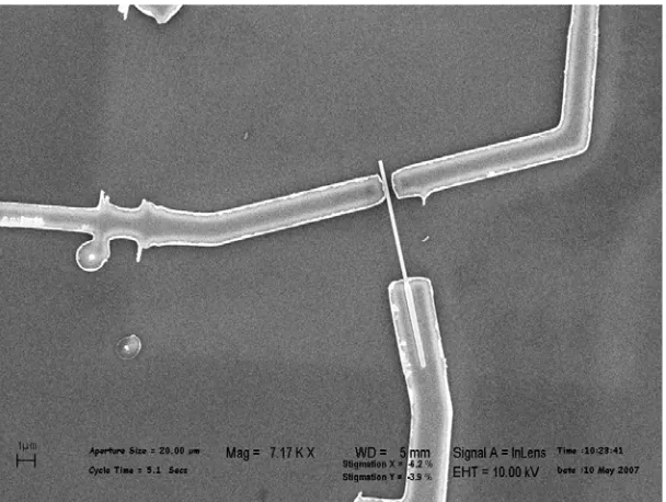
precisely read by SEM software, as shown in figure 8,in which the actual area is 27.057
µm by 20.293 µm for this 10,000X image at aperture size of 20µm and working distance
(WD) at 7 mm. The in-situ e-beam nanolithography mainly counts on the quality of the
voltage contrast image and the precision of the field area to minimize the positioning
error, since we cannot control the small vibration of the stage and the electron beam drift.
The in-situ e-beam nanolithography eliminates the stage movement error by preventing
any movements of the stage during the nanolithography; hence, a high precision laser
stage is not needed. The fabrication of alignment marks on the substrate is also not
necessary, which simplifies the traditional lithography process.
15
In a traditional way, aligning electrodes and making contacts to nanowires need
registrations of the positions of the nanowires relative to the alignment marks. The
coordinates of the nanowires are used to pattern contacts to the nanowires using e-beam
nanolithography. Generally the alignment marks are at the corners of the die, and the
target nanowires are far away at the center. The e-beam nanolithography requires the
movement of the stages, so that the electron beam can be centered on the area of interest.
The positioning accuracy can often be jeopardized by ordinary SEM stages movement
accuracy. The accuracy can be better (<0.1 um) when converted SEMs equipped with the
expensive high precision laser stages are used. Currently the commercially available
dedicated e-beam nanolithography system, such as JEOL JBX-9300FS, has an overlay
and stitching accuracy of 20 nm and positional accuracy of 25 nm48. However, such
accurate results can barely be achieved in most research facilities where e-beam
nanolithography is performed through converted electron microscope systems at a small
fraction of the cost of a dedicated system. However, the positioning error in our method
can be minimized to about 10 nm, which is already superior to most of the converted
SEMs equipped with laser stages and can be widely used in nanodevice fabrication in
16
2.4.1 Voltage-contrast imaging for EBL
The contrast mechanism in scanning electron microscope has long been studied49.
By making use of the local potential differences between semiconducting nano-materials
and the insulator substrate, a rapid imaging technique for nanotubes50was developed.
Moreover, an alignment system using voltage contrast images was proposed by Nakasugi
et al.51for low-energy e-beam lithography, which provides the advantages of high
sensitivity, reduced charging, and low proximity and heating effects. To overcome the
disadvantage of short penetration range of electrons in low energy e-beam
nanolithography, many thin film techniques for photoresists were developed 52. Since the
deposited electrodes should be thick enough to clamp and suspend nanowires, we would
like to take advantage of the rapid voltage contrast imaging technique for nanowire
position registration and avoid the draw back from short penetration of the low energy e
-beam nanolithography at the same time.
In our experiment, we tried to implement this idea in two ways: (i) Use low kV for
imaging and high kV for e-beam lithography, (ii) Use mid-level kV for both imaging and
e-beam lithography. The first way was unsuccessful because it was hard to find a precise
image field and working distance matching between low kV imaging and high kV
imaging, which resulted in poor alignment and resolution in e-beam nanolithography.
The second approach led to a little bit poor voltage contrast image as the recommended
voltage contrast imaging conditions are in the incident energy range of 2keV to 4keV53.
However, by shortening the scanning time, an acceptable image was achieved without
17
In figure 9, images from left to right were taken at different scanning times of 350
ms, and 190 ms respectively. All other imaging conditions were kept the same. Evidently,
the less the scanning time is, the better the contrast is. Edge and contrast enhancement on
the image can improve the positioning accuracy as well. Here is an explanation of such
phenomenon. During imaging, the electron beam bombards on the insulating PMMA
surface, then the PMMA is negatively charged54. In this case, the semiconducting
nanowires are positive with respect to the PMMA. Differences in surface electrostatic
potential affect the number of secondary electrons leaving the PMMA. A positive surface
will increase the secondaries, while a negative surface will decrease the number of
secondary electrons. If longer time is taken, the whole image field will tend to be
potential equilibrium, which lowers the contrast. That’s why shorter scanning time would
help us get better contrast.
As the area of interest had been previously exposed for imaging in a short time, the
18
be kept still right from the last imaging till the end of direct writing to achieve better
alignment, which is comparable to the results of a dedicated e-beam system.
2.4.2 Layout editing for positioning accuracy optimization
Layout editing for EBL is a little bit tricky for positioning accuracy optimization.
Before, users of EBL liked to set the lower left corner of the pattern as the origin of the
pattern, this would results in poor positioning due to image distortion at the edge of the
writing field. What’s worse, even with beam blanker, the LEO 1530 VP scanning
electron microscope tends to dump the beam to the lower left corner of the writing field
now and then (figure
10).
Setting the origin to
the center of the
voltage contrast
image is highly
recommended. To
set the origin to the
centre of the image,
the accurate filed size
of the image must
first be set. For a typical 10,000 X magnification image, the filed size is 27.057 µm by
20.293 µm. Then the lower left corner of the image is set to (0,0), so that the upper right
19
which needs to be set as the origin. Without these correct coordinates information,
precise alignment or positioning can barely be achieved. Another advantage of setting the
origin to the center of the image is that higher writing magnification can be set in the run
file. The NPGS support up to 10,000 X writing magnification. The higher the writing
magnification, the better the writing feature and alignment. Besides, if the writing
magnification is not kept the same as that of imaging magnification, the center of the
field would change a little because of magnification change. The NPGS might not be
able to correct this change; hence, the accuracy would be undermined.
2.4.3 Proximity effect
Due to the electron scattering,
the dose delivered by the electron beam
is not confined to the shapes that are
supposed to be exposed, which results
in line-width variations. If two pattern
features are very close to each other,
significant unintentional exposure or
proximity effect would damage the
whole pattern (figure 11). In our
fabrication of nanoswitches, the proximity effect usually ruined the patterns as the
designed face-to-face electrodes are less than 500 nm apart. A number of algorithms have
been developed that can be used to compensate for proximity effect. Generally these
20
distance from the area to be exposed, and subtracts the amount of backscattered exposure
expected.
Proximity correction algorithms usually describe the scattered beam as a double
Gaussian:
𝐼𝐼
=
𝐼𝐼
0[
𝑒𝑒
− 𝑟𝑟 22𝛼𝛼2
+
𝛾𝛾
𝐸𝐸
𝑒𝑒
− 𝑟𝑟2
2𝛽𝛽2
]
where α is the proximity parameter for forward scattering, β is the proximity parameter
for backward scattering, and
𝛾𝛾
𝐸𝐸 is the ratio of energy deposited due to backscattering tothe energy deposited due to the forward scattering.55 These parameters depend primarily
on the resist used, the underlying substrate and most importantly the accelerating voltage.
Often these parameters are found by performing Monte Carlo simulations. Once the beam
spreading is known the deposited energy at each point can be determined and the dosage
map can be adjusted until all points uniformly exposed.
If the feature size is larger than 1 μm, multiple resist layers can be employed to
minimize the proximity effect and achieve sharp electrode edges. However, the proximity
effect can be used to minimize the face-to-face electrode distances in our case, even
though enough empirical data need to be gathered to estimate the line width variation. In
layout editing, larger gaps of over 200 nm are designed, but line-width variation caused
by the proximity effect will further minimize the actual gaps down below 100 nm.
2.5 Results and discussion
After the nanoswitch fabrication, the samples were treated using oxygen plasma
21
electromechanical nanoswitch characterizations were carried out in the vacuum chamber
(6 x 10⁻⁶ Torr) at room temperature. The test points on the nanoswitches were connected
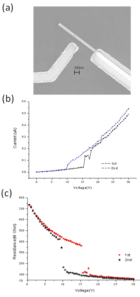
to the electrical probes of the in-chamber micromanipulators, so that the signals can be Figure 12 (a) SEM image of a one-way ZnO nanowire
22
sent and received from a computer-controlled Keithley 2400 outside the chamber. Two
electrical leads were fabricated for a one-way switch and the electrode suspending the
nanowires was connected to the ground while the deflection electrode pulling the end of
the nanowire electro-statically was connected to the applied voltage. The voltage was
scanned back and forth from 0 to 10 V, and the currents flowing through the nanowires
were also recorded simultaneously. As the bias increased, the accumulated attractive
electrostatic force deflected the nanowires toward the facing electrodes to establish an Figure 13(a) SEM image of a one-way Ni nanowire switch (the scale
23
electrical contact, resulting in a sudden jump of current, namely a sharp drop in the
resistance. In Figure 12(a), a 200 nm bending gap in the one-way switch was fabricated
using above procedure, where the diameter of the suspended ZnO nanowire is 150 nm.
The ON and OFF states of the nanoswitch can be clearly identified from the I-V curve in
figure 12(b) and R-V curve in
figure 12(c), respectively. At the
OFF state, as the bias voltage
increases, the resistance
gradually decreases because
more electrons can tunnel
through the SiO2 layer or the air
under higher bias voltage. At the
ON state, the resistance slowly
stabilizes as the electrical
contact becomes better since the
deflected nanowire presses
against the electrode much
harder at higher bias voltage.
Due to the low conductance of
our ZnO nanowire, the ON and
OFF conductance ratio is about
5:1, as shown in Figure 12(c). It is worth noticing that the turn-on threshold varies since
the contact between ZnO nanowire and the electrode can hardly be perfect at the touching
24
employed to make a one-way nickel metal nanoswitch, as shown in figure 13(a). The
diameter of the nickel nanowire is around 200 nm with suspended length around 2 µm. A
bias voltage between 5 V and 7 V could turn on the metal nanoswitch. The rough surface
of the electrode causes the slow transition from OFF state to ON state. However, the
nickel nanoswitch has better conductance at the ON state which makes leakage current
negligible at the OFF state. The ON/OFF conductance ratio of the nickel metal
nanoswitch is over 100. A two-way ZnO nanoswitch was also fabricated as shown in
figure 14 (a). There was a 10 nm positioning error during in-situe-beam nanolithography
process, causing a 10 nm shifting of the both electrodes to the right side and leaving the
left gap about 20 nm smaller than the right one. Figure 14 (b) shows the I-V
measurements of the left way nanoswitch. Since the spacing between the horizontal and
the vertical (center) electrode was only about 500 nm, the OFF state leakage current
showed kind of big. What made the ON/OFF conductance ratio worse was that the
nanowire we patterned had higher resistivity (10Ωcm). Normally, the ZnO nanowire
resistivity ranges from 10-3 to 105Ωcm 56.
To rule out the field emission at ON state, a ZnO nanowire patterned as a field
emission structure, as shown in figure 15 (a), was fabricated using the similar method.
The gap between the tip of the nanowire and the electrode with an applied field is about
200 nm. In the first voltage sweeping, the applied voltage was increased up to 200 V, the
emission current was not observed as shown in the blue curve of figure 15 (b). It is
necessary to apply a voltage close to 210V to trigger the emission of the nanowires as
shown in the red curve of figure 15(b). Based on this result, we can deduce that the
25
individual ZnO nanowires were done by Huang Y H et al.57 Therefore, a turn-on voltage
of less than 10 V in our nanoswitches can hardly trigger the field emission effect for the
suspended ZnO nanowires.
26
Chapter 3 In-situ measurements for one dimensional nano materials
characterization
3.1 In-situ SEM technology for nano-material characterization
Even though the in-situ EBL can easily fabricate many device structures, the
small quantity and manual fabrication makes it unfavorable in the exploration stage of
understanding the
electrical and
mechanical properties
of the nanomaterials.
Meanwhile, the
capability to
manipulate features in
sub-micron range is
quite attractive and
desirable when the electromechanical property of the materials is unknown. While most
of the time SEM is used passively to observe complicated structures at high resolution, a
probe system integrated into the SEM chamber can allow us interact with the samples
directly. With the capability, some unknown properties of the materials have been
discovered58. Other than electrical probing and nanomanipulation, in-situ SEM can as
well be applied in materials science for sample preparation and mechanical
characterization.
27
3.2 Tools for in-situ SEM nano-material characterization at AMRI
The Kleindiek MM3A –EM
mircromanipulator is as shown in figure
16. The movement of the robotic arm is
driven by two rotation motors M1 and
M2, which control the horizontal and
vertical movements, respectively. The
third built-in robot controls the in-out
movement of the tips, so that the probe
tip has 3-freedom movements. Six levels
of the movement speed, vibration
amplitude and frequency can be
configured in the controller (figure 17).
The resolution of horizontal, vertical and
in-out movement are 5nm, 3.5nm and
0.25nm, respectively. The
micromanipulators were fixed to the stage
and then screwed to the SEM rotation
stage during experiments (figure 18).
3.3 Experimental
The in-situ manipulation and electrical probing requires proficiency of operation
of SEM and correct sample placement. Generally, tip preparation and contact preparation
must be done before characterization.
Figure 17 Kleindiek MM3A–EM
mircromanipulator controller.
28
3.3.1 Tip preparation
The probe tips with point radius of 100 nm are tungsten tips provided by the
Micromanipulator company (Model: 7X). To remove oxide deposits, the tips need to be
dipped into a normal sodium hydroxide (NaOH) solution for a few seconds, then rinsed
with deionized water and dried by compressed air. The tips are later heated up or flashed
inside the SEM by applying a constant dc current until the contact resistance between the
top points of two tips was stabilized below 500Ω (generally about 10 Ω) .
Electrochemical etching is the common way to fabricate these tips.
3.3.2 Contact preparation
Generally for
objects on solid
substrates, good
contacts can be made
by pressing firmly on
the objects. As in
figure 18, one probe
tip is pressed firmly
on the CuO2 substrate
with many CuO2
nanowires, and the other electrical lead is connected to the substrate using a conducting
sample holder. A linear I-V curve can easily be retreated without any contact preparation.
However, while probing a single nanowire, the contact is a big issue. In a typical
29
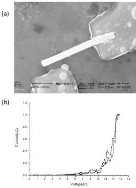
current, while poor contacts resulted in weak signals and large discrepancies between two
measurements. However, for suspended nanowires, good contacts need to be made using
the Joule heating effect assisted by electron gun bombardment36. To demonstrate this
approach, three consecutive I-V characterization were performed on the sample shown in
figure 19 (a). As In figure 19 (b), the first I-V curve was measured while the contact was
first made. By applying 5 V across the nanowire for a few minutes, the second I-V curve
was measured, but still there are large mismatches during back and forth voltage
sweeping despite of the current increase. The heating continued and later the third I-V
curve was getting less mismatches and even stronger current. Generally, an almost linear
I-V curve as shown in figure 20 can be achieved if such routine procedure is kept long
enough.
For an n-type semiconductor, if the work function of the materials is smaller than
the work function of the metal. When contacted, there will be a surface charge region on
30
the contact surface of the semiconductor. The electron density in this region is very small,
showing high resistance and rectifying effect. However, such a contact barrier is also
affected by the surface states density of the semiconductor.
The measured resistance change from G Ω to M Ω fo r o u r Zn O nan owires is
difficult to understand.
Resistance at the
interface may be
reduced as a result of
structure change
leading to a larger
current across the
interface or contact.
The contact surface
states might change as
well, causing lower
contact barrier between probe tips and ZnO nanowires. Larger current generates more
heat and further lowers the contact resistance. As the contact resistance decreases, the
voltage drop at the contact is lower; finally, a balance is achieved and a stable current
level is reached. It is not simply a heating effect. A suitable model has not been reported
for explaining such phenomenon yet.
31
3.3.3 Manipulation of objects
Using probe tips for manipulation has many limitations. Generally without large
separating force, the tip and objects can be bonded together by Vander Wall force. Such
bonding can be improved if the extra current induced heating can melt the joint a little bit.
However, in large angle manipulation, electron beam induced deposition of amorphous
carbon around the contact area is needed to maintain the contact during nanowire
manipulation. Fine step mode should be activated to avoid large abrupt movement of the
probe. To have better control over the movement of samples, special tools like grippers,
rotating tips and some microscope-compatible adhesive chemicals are necessary.
32
3.3.4 In-situ gripping and characterization of the cross-section resistance of one-dimensional nano materials
By using two tungsten probe tips at the same time, a single nanowire can be
gripped and removed from the nanowire arrays. The first probe tip needs to be moved to
the suspended end of the nanowire. By trying to bend the nanowire, it can be told whether
the tip and the nanowire are at the same Z level. After that the nanowire can be bent by
the first tip, the second probe tip is moved to touch the first tip, so that 2 probe tips and
the nanowire are at the same Z level. Then, one tip bends the nanowire towards the
second tip until the nanowire is sandwiched in between. To separate the nanowire from
-6 -4 -2 0 2 4 6
-0.25 -0.20 -0.15 -0.10 -0.05 0.00 0.05 0.10 0.15 0.20
C
ur
rent
(uA
)
Voltage(V)
33
the substrate, the substrate is moved away slowly, while the nanowire and the probe tips
are kept still. Now that the nanowire is gripped by two probe tips (figure 21), the cross
section measurement can be carried out. The contacts still have to be optimized using the
routine procedure mentioned above. The I-V characterization of the cross-section of the
ZnO nanowire shown above is graphed in figure 21. Though the diameter is as small as
150nm, the cross-section resistance is almost as high as that of the longitudinal axis
resistance of that nanowire. Another ZnO nanowire as shown in figure 22 shows
approximately the same high resistance in cross-section. Such a method might be more
suitable for metallic materials measurement rather than the semiconductor measurement
as far as the reliability of the metal-semiconductor contact and relatively small spacing
34
3.3.5 Contact effect study of single ZnO nanowire using in-situ electrical characterization
The versatile nanodevices applications by combining the piezoelectric property
and the semiconducting property of the ZnO nanowire draw lots of attention recently. On
the surface of a deforming nanowire, the potential was non-uniformly distributed due to
the piezoelectric effect59. That makes it
interesting to study how the
measurement results of the ZnO
nanowire would be affected by the
measurement contact points on different
locations of the nanowire surface. With
the contact points on the stretched side of
a deformed ZnO nanowire, Zhong Lin
Wang’s group at Georgia Institute of
Technology have demonstrated the concept of piezoelectric gated diodes60 by bending a
single ZnO nanowire. They also first demonstrated the ZnO nanogenerator by changing
the contact point from the stretched side to compressed side using an AFM tip61, which is
under heated discussion these days.
The initial intention was to repeat the nanogenerator experiment using our nano
manipulators in SEM. The reversed biased Schottky contact can be easily formed on the
stretched side of the nanowire (nanowire has positive potential surface), however, as the
tip glides along the surface of the nanowire and reached the compressed point of the
nanowire to form the forward biased Schottky contact. No as-reported mV range
35
manipulators because: 1) the contact between nanowire and the probe is not reliable
enough during movement, which makes it almost impossible to lead charges on the
nanowire surface to our nano-voltmeter; 2) the movement of the probe tips and the
electron beam can create much noises, whose amplitude can easily exceed 1 mV. Hence,
the contact effect is worth studying in advance.
Our study first targeted on the bending induced change of I-V curve symmetry of
the ZnO nanowire, which was suggested to be the consequence of contact barrier change
due to the bending induced piezoelectric potential change. Such phenomenon is supposed
to be observed only when the contact point is located on the stretched side of the ZnO
nanowire, since a positive potential would be induced on the stretched side to form a
barrier between the probe and the nanowire and regulate the current. As the ZnO
nanowires are grown on the aluminum thin foil substrate, the ohmic contacts are naturally
formed between the nanowire and the substrates. The contact between the probe and
nanowire is optimized using our routine Joule heating plus electron gun bombardment
procedure36. The contact was placed on the underside of ZnO nanowire as schematically
shown in figure 23. Such a contact would provide a way for the induced piezoelectric
charges cancel themselves in place. Hence, there would be little chance to see the gated
36
-6 -4 -2 0 2 4 6
-0.5 0.0 0.5 1.0 1.5 2.0 a b c C u rr ent (uA ) Voltage(V)
5V -5V Rectifying
Ratio
a 2.06uA -0.284uA 7.25
b 2.03uA -0.312uA 6.50
c 1.91uA -0.380uA 5.03
(a)
(b)
(c)
Figure 24 I-V characterization of a deformed ZnO nanowire with the contact on the underside. The rectify ratio was decreasing from (a) to (c) when the bending was being reduced.
Electron beam induced deposition of amorphous carbon was used to maintain the
contact, so that the tip cannot move on the nanowire surface during the experiment. The
nanowire was initially stretched to the right to get the rectifying I-V curves. The currents
at +5V and -5V are 2.06 µA and -0.284 µA, respectively, showing a rectifying ratio of
7.25:1. Slowly the tip was moved to the right a little bit and the bending would be
reduced. Tiny movement step was to make sure the contact point was maintained at the
same location. Three I-V curves were retrieved as shown in figure 24 and they showed
continuous recovering toward symmetry I-V curves.
Under the forward biased, the currents across the nanowire were reducing as the
37
the bending was being released. The rectifying ratio was reduced from 7.25 to 6.51, then
5.03. The linear I-V curve of a straight ZnO nanowire would be changed into a diode-like
I-V curve under bending. Such gated diode phenomenon was first reported by Z. L.
Wang’s group on measurements made on the stretched side of the ZnO nanowire60. The
positive piezoelectric potential induced by bending on the stretched side created a barrier
between the stretched surface and the probe, which rectified the current. Here we found
that such phenomenon can also be observed when contact was made on the underside.
What’s worth mentioning is that the gated diode effect was negligible when the
contact points were on the compressed side. The bending was controlled by moving the
tip leftward. Even though the bending on the nanowire increased, the bending points
actually got away from the contact point, which actually reducing the piezoelectric
surface potential around the contact point. That might be the reason why the rectifying
ratio steadily decreased from 1.99 to 1.36 then 1.26. The last pulling out movement made
the contact point closer to the bending point, which actually increased the rectifying ratio
to 1.56 as shown in figure 25. Such changes in rectifying ratio and the rectifying ratio
amplitudes are far less noticeable compared to those measured on the underside. Another
possible explanation is that the negative surface potential generated by deforming didn’t
affect the contact barrier where electrons were still able to pass freely in both directions.
In that case, there would be no difference in the symmetry of the measured I-V curves no
matter how hard the nanowire is bent.
Same experiments were also carried out on the stretched sides, but the results are
the same with that on the compressed sides. There is another possibility that the as
reported gated diode effect is actually a result of the poor contact between nanowire and
38
diode-like curve after bending released. More experiments with both the piezoelectric
nanowire and non-piezoelectric nanowire should be designed to figure out the mechanism.
As the resistance changes in individual deformed ZnO nanowire have been
employed to fabricate sensors62, it’s worth studying such changes. Two things need to be
considered when we compare the resistance changes. One is the contact resistance and
the other is the piezoelectric resistance of the nanowire itself. It’s hard to study
-7 -6 -5 -4 -3 -2 -1 0 1 2 3 4 5 6 7
-4 -3 -2 -1 0 1 2 3 4 5 a b c d C ur rent (uA ) Voltage(V)
+5V -5V Rectifying Ratio a 3.31 uA -1.66uA 1.99
b 3.36uA -2.45uA 1.37 c 3.25uA -2.58uA 1.26 d 3.71uA -2.38uA 1.56 (a) (b) (c) (d) (e) (f)
39
0 2 4 6 8 10
0 100 200 300 400 500 600 700 800 C ur rent (nA )@ 5V
Time (a. u.)
(a)
0 2 4 6 8 10
50 100 150 200 250 300 350 400 450 C ur rent (nA )@ 5V
Time (a. u.)
(b)
40
piezoelectric resistance alone without taking any contact resistance changes as the gated
diode effect shown above did
lead to changes in current under
the same bias voltage.
To study the
piezoelectric resistance changes
when contact was made on the
underside of the deformed
nanowire forward biased at 5V,
the nanowire was stretched to the
left as shown in figure 26 (a). Slowly the nanowire was moved to the right to increase the
bending. Current drops were observed at each movement which increased the stretching
to the left. Then again the nanowire was slowly moved to the left (figure 26 (b)), which
reduced bending curvature. Current jumps were simultaneously observed at each
movement. The last movement which changed the left stretching into right stretching led
to large current drops instead of current jumps, which indicated that the contact point
might have been moved or the surface polarity of the potential on the contact point might
have been changed. The whole experiment showed the measured resistances of the ZnO
nanowire were increased as the bending curvature increases, even though it’s hard to
calculate how much percentage of the increase was contributed by the contact resistance
changes. The bending induced resistance changes are also employed to make nano
sensors 62,63.
Specifically, a series of characterizations were carried out with the contact point
41
which was trying to separate the tip and the nanowire, made it easy to form the Schottky
contact between the nanowire and the probe. To study the resistance changes with the
Schottky contact, the test need to be made with the nanowire forward biased. First, to test
the stability of the contact, the tip was moved to the right to increase the compressing.
The reversed force of the nanowire became stronger. If the contact point became loose,
the current would drop. However, under forward biased, the current across the nanowire
increased, which meant the contact point was maintained properly. As the nanowire was
released step by step (figure 28), the current dropped accordingly. More compressing on
the nanowire induced lower resistance. Less compressing on the nanowire would induce
higher resistance. Possibly, the contact barrier was lowered by a negative surface
potential rise as the nanowire bending was increased. The last sharp drop was caused by
breaking the nanowire. Even though we tried our best to make sure the manipulation of
the nanowire would not cause movement of the contact point, the contact resistance
might be changed by the surface piezoelectric potential change, which was hard to avoid
in such characterizations. The difficulties in eliminating the contact effect in our
characterization made it hard for us to study relationship between the piezoresistance and
the bending curvature. Still, another possible explanation is that the ZnO nanowires
under study have different polarizations64 and behave differently under bending.
Since the results in figure 24 show behaviors which are close to those of the
Schottky contacts. We assume that the changes are mainly from the barrier height
changes caused by piezoelectricity. According to the thermionic emission theory, the
following equation can describe the I-V characteristics of the tested nanowire under
42
𝐼𝐼
𝑠𝑠
=
𝐴𝐴𝑒𝑒
−𝜑𝜑
𝑝𝑝𝑝𝑝/
𝑘𝑘𝑘𝑘
(
𝑒𝑒
−𝑞𝑞𝑞𝑞
/
𝑘𝑘𝑘𝑘
−
1)
where 𝜑𝜑𝑝𝑝𝑝𝑝 is the potential energy barrier resulting from piezoelectricity, 𝐼𝐼𝑠𝑠 is the
reverse saturation current, V is the applied voltage, q is the electron charge, k is the
Boltzmann constant 8.617 × 10⁻⁵eVKK−1), T is the absolute temperature, and A is a
constant60. We consider the current at -5V and room temperature with different bending
degrees. With 0 degree bending degree, the current is assumed to be the same as that at
+5V, which is about 2 μA for nanowire in figure 24. In addition, at 0 degree bending, the
piezoelectric potential is zero, i.e. 𝜑𝜑𝑝𝑝𝑝𝑝 = 0 . Then, we can get
𝐼𝐼𝑠𝑠0 = 𝐴𝐴𝑒𝑒−
𝜑𝜑𝑝𝑝𝑝𝑝
𝑘𝑘𝑘𝑘 �𝑒𝑒−𝑘𝑘𝑘𝑘𝑞𝑞𝑞𝑞 −1�=𝐴𝐴 �𝑒𝑒−𝑞𝑞𝑞𝑞𝑘𝑘𝑘𝑘 −1�= 2𝜇𝜇𝐴𝐴.
At condition a of figure 24, 𝐼𝐼𝑠𝑠𝑠𝑠 =𝐼𝐼𝑠𝑠0𝑒𝑒−𝜑𝜑𝑝𝑝𝑝𝑝𝑘𝑘𝑘𝑘 = 2𝜇𝜇𝐴𝐴×𝑒𝑒−𝜑𝜑𝑝𝑝𝑝𝑝𝑘𝑘𝑘𝑘 = 0.284𝜇𝜇𝐴𝐴, which
gives 𝜑𝜑𝑝𝑝𝑝𝑝=0.0505eV. In the same way, we get the piezoelectric potential energy barrier
reduced to 0.048eV and 0.0429eV for condition b and c, respectively.
For the I-V curves in figure 28 (a), a Metal-Semiconductor-Metal model65 is used
to estimate the barrier change. At the initial bending, the contact barrier is estimated to be
0.595 eV, and lowered to 0.584 eV as more bending gets the compressed surface more
negatively charged.
The bending induced resistance increases are also found by in-situ transmission
microscopy66,67. In many of our in-situ experiments, no resistance changes by bending
were observed if the contacts hadn’t been optimized till the current through the nanowire
show signs of saturation. Since the identification and elimination of artifacts are
43
-6 -5 -4 -3 -2 -1 0 1 2 3 4 5 6
0 2 4 6
(2) (1)
C
ur
rent
(uA
)
Voltage(V)
(a)
0 2 4 6 8 10
0 1 2 3 4 5
C
ur
rent
(uA
)@
5V
Time (a. u.)
(b)
44
Chapter 4 Conclusion
In conclusion, we demonstrate a precise voltage-contrast image aided positioning
during in-situ e-beam nanolithography through the fabrication of suspended nanowire
based nanoswitches. The method of sandwiching the nanowires between two layers of
photoresist effectively simplifies the fabrication process of the suspended structure. The
positioning error can be reduced to 10 nm in our fabrication, which is sufficient for most
NEMS fabrications. Details on using rapid voltage-contrast imaging to register the
location of the nanowires without exposing the photoresist have been discussed. Layout
editing for positioning optimization has also been covered. The measurements on
different nanoswitches in the FESEM vacuum chamber present well-defined ON and
OFF states induced by changing the applied voltages, which also proves the reliability of
as-demonstrated process. This simplified process provides an easy, low cost and less time
consuming route to integrate suspended nanowire based structures using a converted
FESEM e-beam system, which can also be customized to fabricate multi-layer structures
for nanodevice applications.
The in-situ measurements using manipulators in SEM has been demonstrated to
study the ZnO piezoelectronics, which is under heated discussion. Our in-situ
measurements of the ZnO nanowire show that the contacts affect the measurements,
which might be the reason that the results are not consistent. Special attentions need to
45
References
1
L. A. W. Robinson, S. B. Lee, K. B. K. Teo, M. Chhowalla, G. A. J. Amaratunga, W. I. Milne, D. A. Williams, D. G. Hasko, and H. Ahmed, NANOTECHNOLOGY, 290-293 (2003).
2
R. Long, J. Chen, J. Lim, Y. Yao , J. Wiley and W. Zhou (accepted by Nanotechnology for publication, 2009).
3
R. Long, K. Wang, J. Chen, and W. Zhou (Preparing for submission). 4
M. S. Bobji, J. B. Pethica, and B. J. Inkson, Journal of Materials Research 20,
2726-2732 (2005). 5
X. G. Ma and K. Komvopoulos, Journal of Materials Research 20, 1808-1813 (2005).
6
A. M. Minor, E. T. Lilleodden, E. A. Stach, and J. W. Morris, in In-situ transmission electron microscopy study of the nanoindentation behavior of Al, 2002 (Minerals Metals Materials Soc), p. 958-964.
7
T. Ohmura, A. Minor, K. Tsuzaki, and J. W. Morris, in Indentation-induced deformation behavior in martensitic steel observed through in-situ nanoindentation in a transmission electron microscopy, 2006 (Trans Tech Publications Ltd), p. 239-244.
8
J. S. Robach, I. M. Robertson, B. D. Wirth, and A. Arsenlis, Philosophical Magazine 83, 955-967 (2003).
9
F. Delmas, M. Vivas, P. Lours, M. J. Casanove, A. Couret, and A. Coujou, Materials Science and Engineering a-Structural Materials Properties Microstructure and Processing 340, 286-291 (2003).
10
D. Baither, T. Krol, and E. Nembach, in Dislocation processes in precipitate-free zones in NIMONIC PE16 studied by in situ transmission electron microscopy, 2004 (Elsevier Science Sa), p. 163-166.
11
K. Hattar, J. Han, M. T. A. Saif, and I. M. Robertson, Journal of Materials Research 20, 1869-1877 (2005).
12
S. G. Pyo and N. J. Kim, Journal of Materials Research 20, 1888-1901 (2005). 13
A. Kroger, R. Wernhardt, C. Somsen, G. Eggeler, and A. Wieck, in In situ transmission electron microscopy-investigations on the strain-induced B19 '-phase in NiTi shape memory alloys structured by focused ion beam, 2006 (Elsevier Science Sa), p. 513-516.
14
J. Olbricht, M. F. X. Wagner, A. Condo, A. Dlouhy, C. Grossmann, A. Kroger, C. Somsen, and G. Eggeler, International Journal of Materials Research 99, 1150-1156 (2008).
15
N. Zarubova, J. Gemperlova, V. Gartnerova, and A. Gemperle, in Stress-induced martensitic transformations in a Cu-Al-Ni shape memory alloy studied by in situ transmission electron microscopy, 2008 (Elsevier Science Sa), p. 457-461.
16
T. Sumitomo, H. Kakisawa, Y. Owaki, and Y. Kagawa, Journal of Materials Research 23, 1466-1471 (2008).
17
D. Baither, V. Mottles, and E. Nembach, Journal of Materials Research 20, 1722-1727 (2005).
18