International Journal of Research (IJR)
e-ISSN: 2348-6848, p- ISSN: 2348-795X Volume 2, Issue 05, May 2015Available at http://internationaljournalofresearch.org
Optimized Design and Implementation of Ieee-754 Floating
Point Processor
GOLLA Srinivasulu.
Mr.G.Rajesh
Dr.V.Trimurthulu,
M-tech (vlsi),Dept of ECE Associate prof,Dept of ECE Hod Of Dept of ECE,CREC, Tirupati., CREC, Tirupati., CREC, Tirupati.,
[email protected] [email protected] [email protected]
Abstract
With this document, we have proposed a complete simulation model of Double precession Floating Point Unit based on IEEE-754 Standard. Lot of real time applications such as financial transactions, Digital Signal Processing, Real time embedded systems, super computers etc., needs a very high speed floating point units. The use of floating point unit has lot of application. This paper presents the design and implementation of high speed floating point unit in FPGA. The Verilog RTL description of proposed work is successfully implement on Virtex -5 FPGA.
Key Words:
IEEE -754 Standard; Floating Point Unit; RTL Description and Virtex – 5 FPGA.
Introduction
Complex number arithmetic is very familiar and significant requirement in almost all Signal Processor Based algorithms and hence most of the modern Digital Signal processors and advanced computing machines are coming with complex number arithmetic modules. Though DSP processors uses set to floating and floating to set conversions which will support a less dynamic range and less accuracy in order to compromise with the number of data bits used to represent a fixed point equivalent of floating point counterpart while floating to fixed conversion. If a fewer number of data
bits are used to represent fixed- point equivalent of floating point numbers, obviously there will be a compromise for accuracy. To avoid that negotiation and to achieve less number of look-up tables, it is better to prefer the anticipated architecture which can directly perform arithmetic operations on the complex numbers that are represented using 32-bit subset of IEEE floating point format. Some works also tried to perform complex arithmetic using resource sharing and pipelining concepts, by using a single Floating point adder and floating point multiplier for processing of both real and imaginary parts to implement a typical bench mark standards. The proposed journey is always a critical task to encounter Latency; meanwhile several architectures had been proposed to overcome this task to implement Floating Point Units in the target devices.
International Journal of Research (IJR)
e-ISSN: 2348-6848, p- ISSN: 2348-795X Volume 2, Issue 05, May 2015Available at http://internationaljournalofresearch.org
The IEEE-754 defines the standard for single-precision and double-precision formats. The range & precision of numbers that can be represented using IEEE-754 format is higher than that of fixed point representation with the same number of bits. Execution of arithmetic operations forIEEE floating-point standard in hardware becomes a critical part of almost all processors. The applications are always looking for high-performance and area efficient execution of floating-point arithmetic operation. Because of Advent development of VLSI trends these days we had encouraged with very high speed FPGA units which makes them to sustain implementation of high speed floating point units and becomes sophisticated environment for real time scientific applications.
The proposed architecture is designed with large amount of data base and its controls so that it could accumulate more than eight million test input data of each 64 bit.
The suggested design is implemented in Verilog HDL and synthesized for Xilinx virtex-5 device. The design is synthesized using Xilinx 14.4 VivadoISE tool.
TABLE 1
SUMMARY OF DESIGN CONSIDERATIONS
Sno Design consideration Selection
1 Compiler Xilinix14.4Vivado
2 Programming
Language Verilog
3 Standard IEEE 754
4 FPGA Virtex -5
5 Interface USB
6 Database More than
8Million test inputs
Modeling OF Double Precision FPU
with FPGA
IEEE 754 specifies three types or Formats of floating-pointnumbers:Single (FORTRAN’s REAL*4, C's float), Double(FORTRAN’s
REAL*8, C's double)and
Double-Extended(FORTAN’s REAL*10+, C's long double).Each format has representations for NaNs (Not-a-Number), ±∞ (Infinity),and its own set of finite real numbers all of the simple form2k+1-Nnwith two integers n ( signed Significand) and k ( unbiased signed Exponent ) that run throughout two intervals determined from the format thus:K+1 Exponent bits: 1 - 2K < k < 2K. N Significant bits: -2N < n < 2N.
Figure1 and figure2 shows the
representation of these floating point numbers separately for single and double precision entities.
International Journal of Research (IJR)
e-ISSN: 2348-6848, p- ISSN: 2348-795X Volume 2, Issue 05, May 2015Available at http://internationaljournalofresearch.org
Figure2: Double precision floating point number
This short depiction 2k+1-N n, only one of its kinds to IEEE 754, is deceivingly simple. At first sight it appears potentially confusing because, if n is even, dividing n by 2 (a right-shift) and then adding 1 to k makes no difference. Whenever such an uncertainty could arise it is resolved by minimizing the exponent k and thereby maximizing the magnitude of Significand n ; this is known as “ Normalization ” which, if it succeeds, permits a Normal nonzero number to be expressed in the form 2k+1-N n = ±2k ( 1 + f ) with a nonnegative fraction f < 1 .Besides these Normal numbers, IEEE 754 has Subnormal (Denormalized) numbers lacking or suppressed in earlier computer arithmetic’s; Subnormal, which permit Underflow to be Gradual, are nonzero numbers with an normalized Significand n and the same minimal exponent k as is used for 0 :Subnormal 2k+1-N n = ±2k (0 + f ) has k = 2 - 2K and 0 < | n | < 2N-1 , so 0 <f < 1 .Thus, where earlier arithmetic had conspicuous gaps between 0 and the tiniest Normal numbers ±22-2K, IEEE 754 fills the gaps with Subnormal spaced the same distance apart as the smallest Normal numbers. Hence to achieve this design is also incorporated with pre and post normalization blocks.
It is noticed that The IEEE standard has three very important requirements; they are consistent representation of floating point numbers across all machines and adopting the standard, correctly rounded arithmetic and consistent and sensible treatment of exceptional situations such as division by zero.
Proposed Block Diagram:
By considering all above mentioned principles the proposed scheme was verified with Xilinx tolls with FPGA Virtex-5 technology and its methodology is populated as given below
Front-End Modeling:
This phase of implementation contains the following stages simulation using Xilinx 14.4 Vivado suite, synthesis using Xilinx 14.4 bXST and verifying on Virtex – 5 FPGA board.
The intention of double precision floating point unit is to create a fully suggested VLSI architecture for advanced processor architectures. The proposed architecture has the following block diagram.
International Journal of Research (IJR)
e-ISSN: 2348-6848, p- ISSN: 2348-795X Volume 2, Issue 05, May 2015Available at http://internationaljournalofresearch.org
Simulation and Synthesis Results
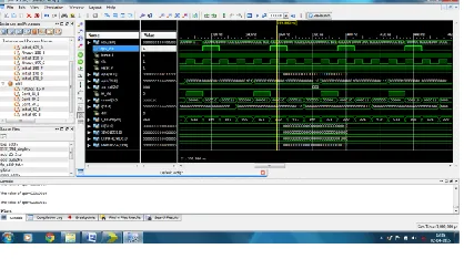
The Verilog RTL Description of the above article is simulated and synthesized using Xilinx14.4 (ISE-Simulator), various results are shown below.Figure7. Simulation output
Figure8. Synthesized output
The Synthesized report is summarized in the following Table.
TABLE 2
SUMMARY OF SYNTHESIS REPORT
Sno Parameter Quantification
1 Target Device xc5vlx50t-2-ff1136
2 Slice Logic utilization 9% 3 Slice logic
distribution 79%
4 IO utilization 21%
5 Specific feature factor 4%
6 Total logic delay 10.314 nS
7 Total offset delay 6.604 nS
8 Total path delay 5.401 nS
9 Real time compilation 120.00 S
10 Total memory usage 548388 Kb
Conclusion
This paper analyzes the complete VLSI Hardware modeling of double precision floating point unit using IEEE-754 standard, this paper has realized with Xilinx tools along with Virtex -5 FPGA such designs are suggested to exhibits a competitive performance with current work.
A
CKNOWLEDGMENTWe would like to thank
Dr.V.THRIMURTHULU, for his
outstanding support and also we would like to especially express gratitude EDUPLUS-IERC team for their technical advices.
References
[1] C. H. Ho, C. W. Yu, P. H. W. Leong,
W. Luk, and S. J. E. Wilton,
Domainspecifichybrid FPGA: Architecture and floating point applications, inProc. Int. Conf. Field Program. Logic Appl. (FPL), 2007,pp. 196201.
[2] Yee Jern Chong and Sri Parameswaran,
Configurable Multimode
EmbeddedFloating-Point Units for FPGAs, IEEE Transactions 2010.
[3] A. Akkas, Dual-mode quadruple precision floating-point adder, in Proc.9th Euromicro Conf. Digit. Syst. Des. (DSD), 2006, pp. 211220.
[4] Xilinx Inc., Virtex-5 Family Overview - LX, LXT,and SXT Platforms,2007.
[5] P. C. Diniz and G. Govindu, Design of a field-programmable dualprecisionfloating-point arithmetic unit, in Proc. Int. Conf. Field Program.Logic Appl. (FPL), 2006, pp. 14.
[6] ANSIWEE std 754-1985, IEEE standard for binary Floating-point arithmetic,IEEE New York (1985)
Luk.TheCoarse-International Journal of Research (IJR)
e-ISSN: 2348-6848, p- ISSN: 2348-795X Volume 2, Issue 05, May 2015Available at http://internationaljournalofresearch.org
Grained/Fine- Grained Logic Interface with Embedded Floating-Point Arithmetic Units. International Journal of Reconfigurable Computing,2008, Article ID 736203, 10 pages, 2008.
[8] Earl E. SwartzlanderJr.,andHani H.M. Saleh, FFT Implementation withFused
Floating-Point Operations, IEEE
Transactions on computers, vol.61no.2, february 2012
[9]Efficient Implementation Of Single Precision
Floating Point Processor, International Conference on Magnetics, Machines & Drives (AICERA-2014 iCMMD)
AUTHORS
GOLLA SRINIVASULU received his B.Tech degree in Electronics & Communication Engineering from Shree Institute of Technical education Tirupathi (A.P), India, in the year 2012. Currently pursuing his M.Tech degree
in VLSI System Design at
ChadalawadaRamanamma Engineering
College,Tirupati(A.P), India.. His area of research Includes in low power vlsi design.
GUNDLAPALLE
RAJESH is currently
working as Associate professor in the Dept.,of elcetronics&communication engineering at Chadalawada Ramanamma Engineering College, near tirupati, india. He has nearly 11 years of teaching experience. His extensive education includes B.tech. From Jawaharlal
technological university, Hyderabad,india, plus m.e. in Satyabama University, Chennai, india. In addition to this, he is making research in the field of medical image processing.
DR.V.THRIMURTH ULU M.E., Ph.D.,
MIETE., MISTE
Professor & Head of
ECE Dept. He
received his
Graduation in
Electronics & Communication Engineering AMIETE in 1994 from Institute of Electronics & Telecommunication Engineering, New Delhi, Post Graduation in Engineering M.E specialization in Microwaves and Radar Engineering in the year Feb, 2003, from University College of
Engineering, Osmania University,