International Journal of Research (IJR)
e-ISSN: 2348-6848, p- ISSN: 2348-795X Volume 2, Issue 09, September 2015Available at http://internationaljournalofresearch.org
An Advanced No isolated High-Efficiency Single-Input
Multiple-Output Converters
Sk.Reshma*
1; Tajuddin Sayyad
2& Dr. Abdul Ahad
31M.tech (PI&D) Student Department Of EEE, Nimra College Of Engineering & Technology
2 Asst. Professor Department Of EEE, Nimra College Of Engineering & Technology
3Professor & Head Of The Department, Nimra College Of Engineering & Technology
ABSTRACT:
The aim of this study is to develop a high-efficiency single-input multiple-output (SIMO) dc–dc converter. In a photovoltaic (PV)- or fuel-cell-based grid connected power system, a high step-up dc–dc converter is required to boost the low voltage of a PV or fuel cell to a relatively high bus voltage for the
downstream dc–ac grid-connected inverter. The proposed converter can boost the voltage of a
low-voltage input power source to a controllable high-low-voltage dc bus and middle-low-voltage output terminals. Moreover, middle-voltage output terminals can supply powers for individual middle-voltage dc loads or for charging auxiliary power sources (e.g., battery modules). In this study, a coupled-inductor based dc– dc converter scheme utilizes only one power switch with the properties of voltage clamping and soft switching, and the corresponding device specifications are adequately designed.
INTRODUCTION
In Order to protect the natural environment on the earth, the development of clean energy without pollution has the major representative role in the last decade. By dealing with the issue of global warming, clean energies, such as fuel cell (FC), photovoltaic, and wind energy, etc., have been rapidly promoted. Due to the electric characteristics of clean energy, the generated power is critically affected by the climate or has slow transient responses, and the output voltage is easily influenced by load variations. Besides, other auxiliary components, e.g., storage elements, control boards, etc., are usually required to ensure the proper operation of clean energy. In
this project presented a SIMO dc–dc converter capable of generating buck, boost, and inverted outputs simultaneously. However, over three switches for one output were required. This scheme is only suitable for the low output voltage and power application, and its power conversion is degenerated due to the operation of hard switching.
International Journal of Research (IJR)
e-ISSN: 2348-6848, p- ISSN: 2348-795X Volume 2, Issue 09, September 2015Available at http://internationaljournalofresearch.org
DC TO DC CONVERTERS
DC to DC converters are important in portable electronic devices such as cellular phones and laptop computers, which are supplied with power from batteries primarily. Such electronic devices often contain several sub-circuits, each with its own voltage level requirement different from that supplied by the battery or an external supply (sometimes higher or lower than the supply voltage). Additionally, the battery voltage declines as its stored power is drained. Switched
DC to DC converters offer a method to increase voltage from a partially lowered battery voltage thereby saving space instead of using multiple batteries to accomplish the same thing. Most DC to DC converters also regulate the output voltage. Some exceptions include high-efficiency LED power sources, which are a kind of DC to DC converter that regulates the current through the LEDs, and simple charge pumps which double or
triple the output voltage.
International Journal of Research (IJR)
e-ISSN: 2348-6848, p- ISSN: 2348-795X Volume 2, Issue 09, September 2015Available at http://internationaljournalofresearch.org
Fig.1 characteristics of proposed SIMO converter
Operating Modes
Mode 1 (t0-t1)
Mode 2 (t1-t2)
Mode 3 (t2-t3)
Mode 4 (t3-t4)
Mode 5 (t4-t5)
Mode 6 (t5-t6)
Operating Modes Explanation
MODE 1 (t0-t1)
International Journal of Research (IJR)
e-ISSN: 2348-6848, p- ISSN: 2348-795X Volume 2, Issue 09, September 2015Available at http://internationaljournalofresearch.org
The secondary current iLs reverses and charges to the middle voltage capacitor C2. When the auxiliary inductor Laux releases its stored energy completely, and the diode D2 turns OFF, this mode ends.
Fig.2 operating mode (t0-t1)
MODE 2 (t1-t2)
At time t = t1, the main switch S1 is persistently turned ON. Because the primary inductor LP is charged by the input power source, the magnetizing current iLmp increases gradually in an approximately linear way.
At the same time, the secondary voltage vLs charges the middle-voltage capacitorC2 through the diode D3.
Although the voltage vLmp is equal to the input voltage VFC both at modes 1 and 2, the ascendant slope of the leakage current of the coupled inductor (diLkp /dt) at modes 1 and 2 is different due to the path of the auxiliary circuit.
Because the auxiliary inductor Laux releases its stored energy completely, and the diode D2 turns OFF at the end of mode 1, it results in the reduction of diLkp /dt at mode2.
Fig.3 operating mode (t1-t2)
MODE 3 (t2-t3)
At time t = t2 , the main switch S1 is turned OFF. When the leakage energy still released from the secondary side of the coupled inductor, the diode D3 persistently conducts and releases the leakage energy to the middle-voltage capacitor C2.
International Journal of Research (IJR)
e-ISSN: 2348-6848, p- ISSN: 2348-795X Volume 2, Issue 09, September 2015Available at http://internationaljournalofresearch.org
At the same time, partial energy of the primary-side leakage inductor Lkp is transmitted to the auxiliary inductor Laux, and the diode D2 conducts.
Thus, the current iL aux passes through the diode D2 to supply the power for the output load in the auxiliary circuit.
When the secondary side of the coupled inductor releases its leakage energy completely, and the diode D3 turns OFF, this mode ends.
Fig.4 operating mode (t2-t3)
MODE 4 (t3-t4)
At time t = t3, the main switch S1 is persistently turned OFF.
When the leakage energy has released from the primary side of the coupled inductor, the secondary current iLS is induced in reverse from the energy of the magnetizing inductor Lmp through the ideal transformer, and flows through the diode D4 to the HVSC.
At the same time, partial energy of the primaryside leakage inductor Lkp is still persistently transmitted to the auxiliary inductor Laux, and the diode D2 keeps conducting.
Moreover, the current iL aux passes through the diode D2 to supply the power for the output load in the auxiliary circuit.
Fig.5 operating mode (t3-t4)
MODE 5 (t4-t5)
At time t = t4, the main switch S1 is persistently turned OFF, and the clamped diode D1 turns OFF because the primary leakage current iLkp equals to the auxiliary inductor current iL aux. In this mode, the input power source, the primary winding of the coupled inductor Tr, and the auxiliary inductor Laux connect in series to supply the power for the output load in the auxiliary circuit through the diode D2.
International Journal of Research (IJR)
e-ISSN: 2348-6848, p- ISSN: 2348-795X Volume 2, Issue 09, September 2015Available at http://internationaljournalofresearch.org
MODE 6 (t5-t6)
At time t=t5, this mode begins when the main switch S1 is triggered.
The auxiliary inductor current iL aux needs time to decay to zero, the diode D2 persistently conducts.
In this mode, the input power source, the clamped capacitor C1 , the secondary winding of the coupled inductor Tr , and the middle-voltage capacitor C2 still connect in series to release the energy into the HVSC through the diodeD4. Since the clamped diodeD1 can be selected as a low-voltage Schottky diode, it will be cut off promptly without a reverse-recovery current. Moreover, the rising rate of the primary current iLkp is limited by the primary-side leakage inductor Lkp.
Thus, one cannot derive any currents from the paths of the HVSC, the middle-voltage circuit, the auxiliary circuit, and the clamped circuit.
As a result, the main switch S1 is turned ON under the condition of ZCS and this soft-switching property is helpful for alleviating the switching loss.
When the secondary current iLS decays to zero, this mode ends. After that, it begins the next switching cycle and repeats the operation in mode 1.
Fig.6 operating mode (t5-t6)
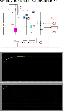
SIMULATION RESULTS & DISCUSSIONS
Fig .7 simulation block dig, output voltages
CONCLUSION
International Journal of Research (IJR)
e-ISSN: 2348-6848, p- ISSN: 2348-795X Volume 2, Issue 09, September 2015Available at http://internationaljournalofresearch.org
the objective of high-efficiency SIMO power conversion; 2) the voltage gain can be substantially increased by using a coupled inductor; 3) the stray energy can be recycled by a clamped capacitor into the auxiliary battery module or high-voltage dc bus to ensure the property of voltage clamping; 4) an auxiliary inductor is designed for providing the charge power to the auxiliary battery module and assisting the switch turned ON under the condition of ZCS; 5) the switch voltage stress is not related to the input voltage so that it is more suitable for a dc power conversion mechanism with different input voltage levels
REFERENCES
[1] A. Kirubakaran, S. Jain, and R. K. Nema, “DSP-controlled power electronic interface for fuel-cell-based distributed generation,” IEEE
Trans. Power Electron., vol. 26, no. 12, pp. 3853–
3864, Dec. 2011.
[2] B. Liu, S. Duan, and T. Cai, “Photovoltaic dc-building-module-based BIPV system-concept and design considerations,” IEEE Trans. Power
Electron., vol. 26, no. 5, pp. 1418–1429, May
2011.
[3] M. Singh and A. Chandra, “Application of adaptive network-based fuzzy interference system for sensorless control of PMSG-based wind turbine with nonlinear-load-compensation capabilities,” IEEE Trans. Power Electron. vol. 26, no. 1, pp. 165–175, Jan. 2011.
[4] C. T. Pan,M. C. Cheng, and C.M. Lai, “A novel integrated dc/ac converter with high voltage
gain capability for distributed energy resource systems,” IEEE Trans. Power Electron., vol. 27, no. 5, pp. 2385–2395, May 2012.
BIBLIOGRAPHY
Shaik Reshma: pursuing M.Tech in Nimra
College of engineering and technology, Jupudi, Ibrahimpatnam. His specialization in power industrial drives. He graduated in Electrical and Electronics Engineering from Nova College of Engineering & Technology , Jupudi. Mail ID
Tajuddin Sayyad: is currently working as an
ASSISTANT PROFESSOR in Electrical and Electronics Engineering department at Nimra College of engineering and technology (NCET) Jupudi, Ibrahimpatnam. He obtained his M TECH degree in Digital systems and computer electronics MAIL ID [email protected]
DR.Abdul Ahad : Mtech. P.hd (NITK) is an