640 | P a g e
The Synthesis & Structural, optical and Electrical
Characterizations of Variation Fluorine Doped tin Oxide
Thin Films by Spray Deposition Techniques
B.L.Khatik
1, Dr. R.N. Arle
2 1Research scholar, JJT University, Rajasthan. (India)
2
Department of Physics, Jijamata College of Science and Arts, Bhende Bk.(India)
ABSTRACT
The Fluorine doped and undoped tin oxide thin films have been prepared by spray pyrolysis from SnCl2
precursor at the substrate temperature of 6000C. The Fluorine doped tin oxide thin films belong to special class oxides that combine high electrical conductivity with high optical transparency. Such transparent Conducting Oxide (TCO) thin films thus an important component for optoelectronic applications. Spray pyrolysis deposition is a simple and relatively low cost technique for thin film preparation. This work comparers the fluorine doped and undoped SnO2 thin films. The effect of fluorine doping on the structural, optical and electrical properties of thin films have been studies. The characterization of samples was carried out by X-ray diffraction, scanning electron microscopy, UV-VIS spectrophotometer and the four probe method. The as-prepared films are polycrystalline with a tetragonal crystal structure. The films have moderate
optical transmission of the pure SnO2 and fluorine doped SnO2 deposited films is71.2% and 73.3%. The
obtained results reveal that the properties of the films are greatly affected by doping levels. These films are
useful as conducting layers in optoelectronics and photovoltaic devices.
Keywords: Pyrolysis; Tin oxide; X-Ray diffraction; Electrical properties and measurements.
I. INTRODUCTION
The FTO thin films have various applications. In recent best use of transparent conducting oxide thin films as
conducting solar window materials in thin film solar cells [1–6], as heat reflectors for advanced glazing in
solar application[7,8] and as gas sensors [9–13]. Tin oxide is the first transparent conductor which is
significantly commercialized [14]. Among the different transparent conductive oxides, SnO2 films doped with
fluorine are most appropriate for use in solar cells, its low electrical resistivity and high optical transmittance.
SnO2 is chemically inert, mechanically hard and can resist high temperatures [5]. Doped or undoped SnO2
can be synthesized by numerous techniques such as thermal evaporation, sputtering [13-17], painting [3, 17],
chemical vapour deposition [18–20], sol–gel coating [17, 21], spray pyrolysis [3, 13] and hydrothermal method.
In this various deposition techniques, the spray pyrolysis is the most essay method for the good thin films
preparation of doped tin oxide because of its simple and inexpensive experimental arrangement. Simple
spray pyrolysis technique is easy of add to various doping materials, reproducibility, high growth rate and
641 | P a g e
In this study, tin oxide and fluorine doped tin oxide (SnO2) thin films were prepared by the spray pyrolysis
technique at substrate temperature of 6000C using precursor solution. This work is to study the relationship
between the doping and undoing levels and some physical properties of SnO2 & SnO2: F thin films such as the
structural, optical electrical and properties.
II. EXPERIMENTAL DETAILS
The fluorine-doped and undoped tin oxide thin films in the present study were prepared using a spray pyrolysis
apparatus. The both Thin films was deposited on a micro slide glass substrate. Dehydrate stannous chloride
(Sncl2:2H2O) was used for making the precursor 0.1.M solution. This precursor was dissolved in 4 mL
concentrated hydrochloric acid (HCl) and then added with methanol served as the starting solution and
ammonium Bifluoride (NH4 HF2) by ranging from 2 ml to 10 ml in step of 2 ml. Other preparative parameters
like nozzle to substrate distance, air flow rate, and substrate temperature (6000C) were kept constant as the
optimized values. The samples were structural properties analyzed with X-rays diffractometr using a
monochromatic radiation Cu-Kα, λ=1.5406 Å at 30 kV, 10 mA in the range of scanning angle 20° < 2θ <
79.99°. Surface morphological analysis of the films was carried out by Scanning electron microscope (SEM).
Four probe set up was used for electrical measurements at room temperature. Optical transmittance spectra of
the films were measured using a PC based, UV-VIS Systronics spectrophotometer in the range 200 nm to 999
nm of wavelength with air as reference.
III. RESULTS AND DISCUSSION
3.1 Structural characterization of tin oxide fluorine doped tin oxide thin films
Tin oxide thin films were prepared by chemical spray pyrolysis technique. The transparency of thin films so
formed depends on parameters like substrate temperature and concentration of the precursor solution. Also other
parameters such as spray duration, flow rate, pressure etc. also affects the features of the thin film. Transparency
and thickness are two important features to be considered. Since the major application area is solar cells
fabrication the thin films must possess high optical transparency and minimum thickness.
Samples of 0.1 M were prepared at 70˚C. The spray duration was set to 1 minute. For this temperature, the films
formed were thick and not transparent, since the decomposition temperature of tin oxide is about 600˚C. Also
the pressure was too high that the substrates were not remaining stationary above the hot plate. Another set of
samples were prepared at a temperature of 600˚C and doped the fluorine concentration. The films formed for
these conditions were better than the first set of samples. The prepared thin films are highly transparent and
conductive films were study for Structural properties.
The high-angle region of XRD pattern of the as-synthesized thin film was used to determine the lattice
parameters ‘a’ and ‘c’ of the tetragonal phase,
By using this equation, we calculated the values of lattice parameter which well matches with JCPDS (Card No.
642 | P a g e
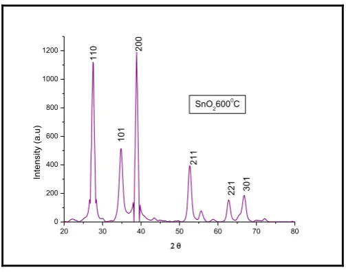
Figure 1 shows the XRD patterns of the Tin oxide thin films at substrate temperature 6000C. The tin oxide thin
film possesses tetragonal rutile structured because its diffraction peaks are clearly observed at 2θ = 26.6°, 33.5°,
37.8° and 51.7°, which corresponding to (110), (101), (200) and (211) directions of the rutile structured SnO2.
The XRD pattern of suggests that average grain sizes of SnO2 thin film synthesized at 6000C are approximately
obtained by using the Scherer formula:
D
Where D = Crystalline grain size,
k = Particle size dependent constant.
λ = is the wavelength for spectrometer radiation (1.54056nm for Cu Kα), β = is the full width at half maximum,
θ = is the scanning angle.
The grain size was calculated to be approximately 9.358 nm
20 30 40 50 60 70 80
0 200 400 600 800 1000
1200 200
301
221
211
101
110
In
te
n
si
ty
(a
.u
)
SnO26000C
Fig. 1 XRD patterns of SnO2 thin films.
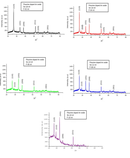
Similarly, compare the XRD patterns of the Fluorine doped Tin oxide thin films (Fig 2.) at substrate temperature
6000C for spray solution 10ml and fluorine doped by ranging from 2 ml to 10 ml in steps of 2 ml. Here SnO2: F
thin films have tetragonal rutile structured because its diffraction peaks are clearly matches. The height of the
peaks increase with increase in the fluorine concentration. A new direction of crystal growth appears
corresponding to the reflection from the (1 1 0), (1 0 1) (2 0 0) and (2 1 1) planes at 2θ = 26.6°, 33.5°, 38° and
51.8°. The presence of other peaks such as (1 1 2), (2 2 0), (3 1 0) and (3 0 1) have also been detected but with
substantially lower intensities at the higher doping concentration. Comparison of interplaner distance (d) values
643 | P a g e
20 30 40 50 60 70 80
200 400 600 800 1000 1200 1400
20 30 40 50 60 70 80
200 400 600 800 1000 1200 1400
20 30 40 50 60 70 80
200 400 600 800 1000 1200 1400
20 30 40 50 60 70 80
200 400 600 800 1000 1200 1400 (11 2) (11 2) (11 2) (11 2) (10 1) (21 1) (20 0) (10 1) (11 0) (30 1) (21 1) (20 0) (11 2) (11 0) (30 1) (21 1) (20 0) (10 1) (11 0) (30 1) (22 0) (21 1) (20 0) (10 1) (11 0) (30 1) (21 1) (20 0) (10 1) (11 0) (22 0)
2 0 3 0 4 0 5 0 6 0 7 0 8 0 9 0
2 0 0 4 0 0 6 0 0 8 0 0 1 0 0 0 1 2 0 0 1 4 0 0 1 6 0 0
I n t e n s it y ( a . u ) 2 Flourine doped tin oxide
Sn-18 ml F-02 ml
Flourine doped tin oxide Sn-10 ml F-10 ml Int en s it y (a. u)
20
Flourine doped tin oxide Sn-16 ml F-04 ml Int en s it y (a. u)
20
Flourine doped tin oxide Sn-14 ml F-06 ml Int en s it y (a. u)
20
Flourine doped tin oxide Sn-12 ml F-08 ml Int en s it y (a. u)
20
Fig. 2 XRD patterns of fluorine doped tin Oxide (SnO2: F) thin films.
644 | P a g e
3.2 Surface morphology of as-prepared films
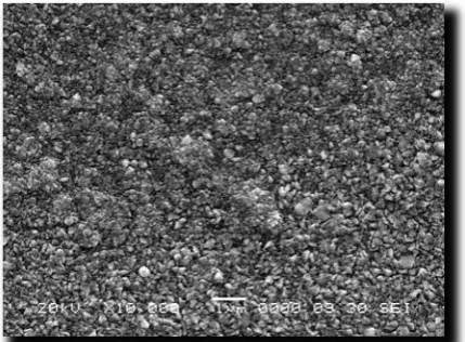
Fig.3 shows a typical SEM micrograph of the tin oxide film deposited at 10 ml solution flow rate. The SEM
microstructures reveal that, all the films have a homogeneous surface morphology with nanocrystalline grains,
also all the films are without any cracks and holes. Patterns indicate that films are polycrystalline in nature. The
EDAX spectra of the same film reveal the elemental analysis, which shows that Sn and O were found to be
89.55: 11.45 in percent.
Fig 3. Typical SEM micrograph of SnO2 thin films.
Fig.4 shows that SEM micrograph of the SnO2: F thin film, fluorine doped by ranging from 2 ml to 08 ml in step
of 2 ml. The SEM microstructures reveal that all the films have a homogeneous surface morphology with
nanocrystalline grains, also all the films are without any cracks and holes. Patterns indicate that films are
polycrystalline in nature and grain size ranges from 150 nm-250 nm.
Fig.4: XRD Pattern for SnO2: F thin film at (a) 2 ml (b) 4 ml(c) 6 ml and (d) 8 ml fluorine concentrations.
3.2 Optical properties
Fig.5shows the variation of optical transmittance spectra in the range 200 nm - 999 nm for the SnO2: F thin
films. From the graph, the films deposited at the substrate temperatures 6000C exhibits highest transmittance in
645 | P a g e
300 400 500 600 700 800 900 1000
0 10 20 30 40 50 60 70 80
Tr
an
smi
ttanc
e (
%)
Wavelength (nm)
Sn-18 ml, F-2 ml Sn-16 ml, F-4 ml Sn-14 ml, F-6 ml Sn-12 ml, F-8 ml Sn-10 ml, F-10 ml
Fig5: Optical Transmittance against wavelength at different
Fluorine concentration of the SnO2 thin films.
Analysis on Optical Band-Absorption Coefficient:-
The analyzing the optical data with the expression for optical absorption coefficient ‘α’ and photon energy ‘hυ’
determine the optical band gap ‘Eg’. Fig.6 (a & b)shows the plot of (αhυ) 2 vs ‘hυ’ .Extrapolation of the linear
portion of the plots to energy axis yielded the direct band gap values of SnO2: F & SnO2 are 3.625eV & 3.60eV
at 6000C respectively.
1.0 1.5 2.0 2.5 3.0 3.5 4.0
0 5 10 15 20
Eg = 3.625 eV
A
bs
or
pt
io
n
co
ef
fic
ie
nt
E
ne
rg
y
Energy (Eg)eV
(a)
1.0 1.5 2.0 2.5 3.0 3.5 4.0
0 5 10 15 20 25 30
A
bsorptio
n
coef
ficient
Energy
Energy (Eg)eV
Eg = 3.630 eV
(b)
646 | P a g e
3.3 Electrical properties
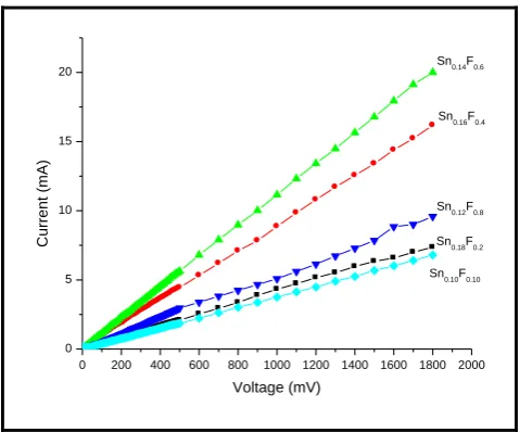
Fig .8 showsthe typical plot of voltage vs current for SnO2: F thin film at room temperature. From the analysis
of the I-V curves, it is observed shows the electrical I-V graph, it is observed that resistivity decrease with
increase of fluorine rate, and more increases fluorine rate also increases resistivity. The calculated resistivity
values are 0.0067, 0.0046, 0.0052, 0.016, 0.033 Ω-cm respectively. The deposited thin films with various
fluorine % such as 10%, 20%, 30%, 40%, 50% respectively.
0 200 400 600 800 1000 1200 1400 1600 1800 2000 0
5 10 15 20
Sn0.10F0.10 Sn0.12F0.8 Sn0.14F0.6
Sn0.16F0.4
Sn0.18F0.2
C
u
rre
n
t
(m
A)
Voltage (mV)
Fig.6 .28 I- V curve of 𝑆𝑛𝑂2: 𝐹 thin films as a function of wavelength for different fluorine doping.
IV. CONCLUSIONS
In this work, SnO2 and SnO2: F thin films grown successfully by spray pyrolysis method. The structural
investigation revealed that the both films are crystalline in nature with corresponding to (110), (101), (200) and
(211) directions of the rutile structured as a preferred orientation with a tetragonal crystal structure. As
deposited films was uniform and strongly adherent to substrate. The average transmittance of the deposited
SnO2 and SnO2: F thin films were about 71.2 % and 73.3 % and optical band gap 3.625 eV & 3.630 eV
respectively. The electrical studies conclude that resistivity decrease with increase in fluorine doping and there
after it increases with increase in doping volume and values are 0.0067, 0.0046, 0.0052, 0.016, 0.033 Ω-cm
respectively