ABSTRACT
RAVURI, LIKHITA. Interactions between Distributed Energy Resources in a Balanced Three-Phase Microgrid . (Under the direction of Dr. Srdjan M Lukic.)
The penetration of Distributed Energy Resources (DER) at medium and low voltages (MV and
LV), both in utility networks and downstream of the meter, is increasing worldwide. While the
application of DERs can potentially reduce the need for traditional system expansion, controlling
a huge number of DERs create a whole new challenge for operating and controlling the network
safely and efficiently. This challenge can be partially addressed by microgrids, that are localized
grids that can disconnect from the traditional grid to operate autonomously and help mitigate grid
disturbances to strengthen grid resilience. This research mainly focuses on two main concerns in
microgrids: 1. The interactions between various DERs in a microgrid and improving the power
quality, and 2. The system response to faults by abiding to IEEE-1547 standards defined by the
utlility.
Studying the interactions between multiple inverter interfaced DERs when tied together is
absolutely important, given their predominance in many microgrids. In order to avoid the need
for any communication among modules in a paralleled inverter system, the power-sharing control
loops are based on the P/Q droop method. The output impedance of the closed-loop inverter affects the power sharing accuracy and determines the droop control strategy. Furthermore, the
proper design of this output impedance can reduce the impact of the line-impedance unbalance. In
order to program a stable output impedance, the virtual impedance concept is increasingly used for
the control of power electronic systems, as an additional degree of freedom for active stabilization,
improved power quality and disturbance rejection. Methods to estimate the optimal values for these
virtual impedances have been explored.
Synchronous generators are one of the most common types of DERs, and this research focuses on
interactions between inverter based DERs and synchronous generators in microgrids. When voltage
inertia is observed to change the system dynamics when compared to the most common
inverter-based microgrids. The operating characteristics of such microgrid systems have been explored for
different modes of operation.
Instead of trying to mitigate inverter overloads and thus allow larger voltage and frequency
transients, it is often preferable to allow the inverter to provide as much support as possible, and
simply current limit when necessary. Also, according to the new IEEE-1547 standards, the smart
in-verters in microgrids are expected to stay online and operate in Low Voltage Ride Through (LVRT)
mode. Current limiting in the presence of other grid-forming DER is complicated for voltage
con-trolled inverters. The use of simple current reference saturation is shown to cause instability. Virtual
impedance current limiting is implemented to provide improved transient stability during current
limiting with faults. Current limiting performance during faults in islanded and grid connected
mode is investigated, and it is shown that virtual impedance current limiting provides improved
transient stability during current limiting in the presence of synchronous generators compared to
traditional current limiting methods.
The methods implemented in this thesis for mitigating the problems with multiple component
interactions in microgrids will allow for more reliable and cost effective application of inverter based
DERs with synchronous generators in the microgrid, even during faults. The analysis was carried
out by modeling the microgrid system using PLECS and MATLAB software platforms. Hardware
validation for the same have been initialized through designing and building a robust DC storage
©Copyright 2017 by Likhita Ravuri
Interactions between Distributed Energy Resources in a Balanced Three-Phase Microgrid
by Likhita Ravuri
A thesis submitted to the Graduate Faculty of North Carolina State University
in partial fulfillment of the requirements for the Degree of
Master of Science
Electrical Engineering
Raleigh, North Carolina
2017
APPROVED BY:
Dr. Iqbal Husain Dr. David Lubkeman
DEDICATION
To my dear parents, Lakshmi and Satyanarayana Ravuri
BIOGRAPHY
Likhita Ravuri was born on May 27, 1995 to Lakshmi Devi and Satyanarayana V.V. Ravuri,
in the city of Bhimavaram (Andhra Pradesh), India. She received the Bachelor of Engineering
(B.E.) with Honors in Electrical and Electronics Engineering from Birla Institute of Technology
and Science (BITS) Pilani, Hyderabad in 2015.
Likhita joined the Electrical and Computer Engineering Department of North Carolina State
University in August 2015 to pursue the Master of Science (M.S.) degree in Electrical
Engineer-ing. She has been working with the Future Renewable Electric Energy Delivery and Management
(FREEDM) Systems Center under the guidance of Dr. Srdjan M. Lukic for the past two years,
during the course of her master’s degree.
Her research interests include Power Electronics and Microgrids. After her graduation, she
plans to join VoltServer as an Electrical Design Engineer and pursue a career in the industry in an
ACKNOWLEDGEMENTS
I would like to thank my advisor, Dr. Srdjan Lukic for giving me the opportunity to work on this
thesis under his guidance. I owe my progress in this work to him for his knowledgeable mentorship
and his ever encouraging belief in me. His leadership, support, attention to detail, and hard work
have set an example I hope to match some day. I sincerely thank him for understanding my
con-straints and supporting me throughout the past 2 years, this wouldn’t have been possible if not for
the confidence he had in me.
My sincere thanks to Dr. Iqbal Husain for efficiently leading the FREEDM Systems Center as
the Director and for his efforts in making the center one of the best Power Electronics research
centers in the world. My heartfelt thanks to Dr. David Lubkeman for his contributions as the leader
for GEH Testbed. I thank him for all the insightful discussions in the course of our preparation
for the NSF Site Visit-2017, it was a one-of-a-kind experience. Special thanks to Dr. Wensong
Yu for leading the LV-SST hardware team for GEH Testbed and for his very informative and
knowledgeable Power Electronics training sessions.
Thank you Hao, for being patient and helping me through the DESD prototyping, especially
with the communication protocols. Thank you for introducing me to the concept of fault analysis in
smart inverters. It was a great pleasure working with you and I am thankful for finding a good friend
in this process. Thanks Awal and Siyuan for all the great ideas to make the site-visit demonstration
a huge success, we make a great team together. Thanks Samir for helping me with the synchronous
generator design. Thanks Ashish for all your help with LaTeX. This is a perfect opportunity to
thank Karen, Hulgize and Rebecca for their efforts to make FREEDM a safe, friendly and exciting
place.
Sravani and Gopi, you guys motivated and pushed me all the way from India. We have come a
long way together. Manila, thanks for always being there no matter what. Radha, FREEDM gave
me an amazing, funny and caring soul-sister, always stay the same. Siddharth and Zhao, I never
I am immensely grateful to all the people who made this research and my graduate study at
NC State a wonderful experience for me, I’m very glad that our paths crossed. I wish everyone of
you, the best.
Chinna Mavayya and Chinnatta, you guys left no stone unturned to ensure my happiness
throughout the past two years. Thank you for being the most caring and awesome uncle and aunt
ever. Tejas, one smile from you would brighten up my day. I express my sincere appreciation to my
extended family, this wouldn’t have been possible without you all.
Amma and Daddy, I am extremely grateful to have you both as my parents. Thank you for
all the sacrifices and your unconditional love. Daddy, the confidence you had in me is what drives
me even today. Thank you for setting up the best example to working hard and staying content.
Amma, I know how hard it has been for you to take care of everything all by yourself for the past
three years, thank you for being strong and motivating me to chase my dreams. Pandu, you are
TABLE OF CONTENTS
LIST OF TABLES . . . .viii
LIST OF FIGURES . . . ix
Chapter 1 Introduction . . . 1
1.1 Big Picture-Microgrids . . . 1
1.2 Problem Statement . . . 3
1.2.1 Component Interactions . . . 3
1.2.2 IEEE 1547 standards during faults (Low Voltage Ride Through) . . . 3
1.3 Objectives . . . 5
1.4 Outline of Chapters . . . 5
Chapter 2 Modeling and Control of Distributed Energy Resources in Microgrid . 7 2.1 Three Phase Battery Energy Storage System . . . 7
2.1.1 Overview of Energy Storage Systems in microgrids . . . 7
2.1.2 Three Phase Inverter Plant . . . 9
2.1.3 DC/DC Stage - Modeling . . . 21
2.1.4 Battery Interface . . . 30
2.2 Inverter based Distributed Generator Emulation . . . 31
2.3 Synchronous Generator Model . . . 32
2.3.1 Modeling . . . 32
2.3.2 Control . . . 32
2.3.3 Permanent Magnet SG Vs. Wound Field SG . . . 38
Chapter 3 Component Interactions in Three-Phase Microgrids . . . 39
3.1 System at Test . . . 39
3.2 Paralleled Inverter System . . . 40
3.2.1 Operation . . . 41
3.2.2 Challenges . . . 45
3.2.3 Virtual Impedance . . . 46
3.2.4 Stability . . . 47
3.3 Generators in microgrids . . . 48
3.3.1 Operation . . . 48
3.3.2 Machine dynamics in a microgrid . . . 48
3.3.3 Effect on Inverters . . . 51
3.4 Connection Type . . . 52
3.4.1 Grid Connected Mode . . . 54
3.4.2 Islanded Mode . . . 58
Chapter 4 Fault Current Limiting in Three-Phase Microgrids . . . 63
4.2.1 Before FCLs . . . 64
4.2.2 Fault Current Limiters . . . 65
4.3 Virtual Impedance based FCL . . . 66
4.3.1 Strategy-1 [1] . . . 67
4.3.2 Strategy-2 [2] . . . 69
4.3.3 Simulation Results . . . 71
Chapter 5 Hardware Development . . . 85
5.1 Hardware Prototyping . . . 85
5.1.1 Converter Hardware . . . 85
5.1.2 Auxiliary Power Supply . . . 87
5.1.3 Final Hardware Prototype . . . 88
5.2 Battery Pack . . . 89
5.2.1 Battery Management System (BMS) . . . 90
5.3 Protection Mechanisms . . . 92
5.3.1 Protection Hardware . . . 92
5.3.2 Software Protection . . . 94
5.4 Experimental Results . . . 94
Chapter 6 Conclusion . . . 99
6.1 Accomplishments . . . 99
6.2 Recommended Future Work . . . 100
6.2.1 Secondary control for Inverters . . . 100
6.2.2 Active current threshold calculation during faults . . . 100
6.2.3 Stability analysis and bounds forZf cl . . . 101
References. . . .102
Appendix . . . .107
Appendix A Virtual Impedance Value Optimization . . . 108
A.1 Virtual Impedance for Real and Reactive Power Decoupling . . . 108
LIST OF TABLES
Table 2.1 Three Phase Inverter-Model Parameters . . . 17
Table 2.2 Interleaved DC/DC Boost Converter-Model Parameters . . . 30
Table 2.3 100kVA Synchronous Generator-Controller Parameters [1] . . . 36
LIST OF FIGURES
Figure 1.1 Microgrid, Adapted from [3] . . . 2
Figure 1.2 Voltage Interconnection and Ride Through requirements, Adapted from [4] . . . 4
Figure 1.3 Frequency Interconnection and Ride Through requirements, Adapted from [4] . . 5
Figure 2.1 3-phase ESS block diagram . . . 8
Figure 2.2 Three Phase Inverter Circuit Diagram . . . 10
Figure 2.3 Three Phase Inverter Controller Block Diagram . . . 17
Figure 2.4 PWM Switching Sequence . . . 18
Figure 2.5 3-Phase Inverter Output Voltage Waveforms . . . 19
Figure 2.6 Three Phase Output Current Waveforms . . . 19
Figure 2.7 Three Phase Inverter Voltage Waveform during Load Change . . . 20
Figure 2.8 Three Phase Inverter Current Waveform during Load Change . . . 20
Figure 2.9 Boost Converter circuit diagram . . . 21
Figure 2.10 Boost Converter - ON State . . . 22
Figure 2.11 Boost Converter - OFF State . . . 22
Figure 2.12 Designed Interleaved DC Energy Storage Device circuit diagram . . . 25
Figure 2.13 DC-DESD current controller bode plot . . . 26
Figure 2.14 Bode plot to determine voltage controller bandwidth . . . 27
Figure 2.15 DC-DESD control loop simulation block diagram . . . 28
Figure 2.16 DC DESD inductor current waveforms: (a)Step response of inductor currents, (b)DC-DESD inductor current ripple in each interleaved phase . . . 29
Figure 2.17 DC DESD battery current ripple . . . 29
Figure 2.18 Battery Model Circuit Diagram [5] . . . 31
Figure 2.19 Synchronous Generator Block Diagram, Adapted from [1] . . . 33
Figure 2.20 Governor Control Circuit Block Diagram . . . 34
Figure 2.21 Governor following the Speed Reference . . . 34
Figure 2.22 AVR Control Circuit Block Diagram . . . 35
Figure 2.23 AVR following the Voltage Reference and applying the corresponding Vf . . . 37
Figure 2.24 3-phase SG terminal voltage and current waveforms during load change . . . 37
Figure 3.1 Microgrid System under test . . . 40
Figure 3.2 Parallel voltage sources concept illustration, Adapted from [6] . . . 41
Figure 3.3 Real Power-Frequency (P-f) and Reactive Power-Voltage (Q-V) Droop charac-teristics . . . 42
Figure 3.4 Three Phase paralelled inverter voltages at PCC . . . 43
Figure 3.5 Three Phase paralelled inverter voltages at PCC . . . 44
Figure 3.6 Power Sharing in Paralleled 3-phase Inverters . . . 45
Figure 3.7 Virtual Impedance Concept [7] . . . 46
Figure 3.8 Paralleled Inverter-Generator voltage waveforms at PCC . . . 49
Figure 3.9 Paralleled Inverter-Generator current waveforms at PCC . . . 49
Figure 3.10 Paralleled Inverter-Generator Real power sharing . . . 50
Figure 3.12 System settling time delay due to SG’s inertia . . . 52
Figure 3.13 Simulated Microgrid System in PLECS . . . 53
Figure 3.14 DER Voltages in Grid connected mode . . . 54
Figure 3.15 DER Currents in Grid connected mode . . . 55
Figure 3.16 Grid Voltage and Currents . . . 55
Figure 3.17 Governor following the Speed Reference in Grid connected mode . . . 56
Figure 3.18 AVR following the Voltage Reference and applying the correspondingVf in Grid connected mode . . . 57
Figure 3.19 Power sharing in DERs in Grid connected mode . . . 57
Figure 3.20 Real power shared by the Grid . . . 58
Figure 3.21 DER Voltages in Islanded mode . . . 59
Figure 3.22 DER Currents in Islanded mode . . . 60
Figure 3.23 Governor following the Speed Reference in Islanded mode . . . 61
Figure 3.24 AVR following the Voltage Reference and applying the corresponding Vf in Is-landed mode . . . 61
Figure 3.25 Power sharing in DERs in Islanded mode . . . 62
Figure 4.1 High-Temperature superconducting FCL [8] . . . 65
Figure 4.2 Solid-state FCL [9] . . . 66
Figure 4.3 Virtual Impedance based Fault current limiting . . . 67
Figure 4.4 Virtual impedance based Fault current limiting strategy . . . 69
Figure 4.5 Phasor Diagram for Impedance . . . 70
Figure 4.6 Three-phase balanced fault at PCC in the current microgrid . . . 71
Figure 4.7 Droop Output for 3-phase balanced fault at t=5.85s to t=6.2s . . . 72
Figure 4.8 DER Voltages during 3-phase Fault at PCC in Islanded mode . . . 73
Figure 4.9 DER Currents during 3-phase Fault at PCC in Islanded mode . . . 74
Figure 4.10 Overall Virtual Impedance in the system during Fault-Islanded mode . . . 75
Figure 4.11 RMS currents in Inverter during 3-phase Fault-Islanded mode . . . 76
Figure 4.12 Power sharing in DERs during 3-phase Fault in Islanded mode . . . 76
Figure 4.13 PWM Generation during Fault . . . 77
Figure 4.14 Governor during Fault in Islanded mode-Speed reference generator . . . 78
Figure 4.15 AVR during Fault in Islanded mode-Applied field voltage . . . 79
Figure 4.16 DER Voltages and Currents during a 3-phase fault at PCC . . . 80
Figure 4.17 RMS currents in Inverters during 3-phase balanced fault at PCC . . . 80
Figure 4.18 Virtual Impedance in the system with a 3-phase balanced fault triggered at t=16.7s to t=17.85s . . . 81
Figure 4.19 Power sharing in DERs during 3-phase balanced fault at PCC in Grid connected mode . . . 82
Figure 4.20 PWM generation during 3-phase balanced Fault at PCC . . . 83
Figure 4.21 Governor following speed reference in Grid-connected mode during 3-phase bal-anced fault at PCC . . . 83
Figure 5.1 SiC Power Module (CCS050M12CM2) [10] . . . 86
Figure 5.2 Interfacing board mounted on top of the Gate Driver board from Cree . . . 86
Figure 5.3 Power Board for DESD . . . 87
Figure 5.4 Auxiliary Power Supply . . . 88
Figure 5.5 Final Converter Hardware with all the auxiliary circuitry . . . 88
Figure 5.6 Battery Module Operation [11] . . . 89
Figure 5.7 Toshiba LTO Battery pack used for the current DESD application . . . 90
Figure 5.8 Battery Management System . . . 91
Figure 5.9 DC-DC Converter Hardware in the DESD rack . . . 92
Figure 5.10 State Machine Algorithm for software protection . . . 94
Figure 5.11 Output Voltage and Currents at No Load operation- Worst Case . . . 95
Figure 5.12 No Load Closed-loop transient of DESD-StepUp . . . 95
Figure 5.13 No Load Closed-loop transient of DESD-StepDown . . . 96
Figure 5.14 3kW load Closed-loop response of DESD . . . 96
Figure 5.15 Inductor Current Ripple for a 3kW Load . . . 97
Figure 5.16 Transient Response of DESD with a 3kW Load . . . 98
Figure A.1 Optimization of virtual impedance for decoupling P and Q . . . 109
Chapter 1
Introduction
1.1
Big Picture-Microgrids
Economic, technology and environmental incentives are revolutionizing electricity generation and
transmission. The generating facilities are slowly moving towards more distributed energy resources
rather than centralized generation. Distributed Energy Resources (DER) include a wide range of
prime mover technologies, such as gas turbines, microturbines, internal combustion (IC) engines,
Photo-Voltaic (PV) systems, fuel cells, wind-power and storage devices. These emerging
technolo-gies have lower emissions and the potential to have lower cost negating traditional economies of
scale [12]. Few applications include power support at substations, deferral of transmission and
dis-tribution upgrades, use of renewable energy, higher power quality and smarter disdis-tribution systems.
Thus, distribution system provides major opportunities for smart grid concepts.
According to a recent research at University of Puerto Rico as part of the GridEd consortium
[13], today’s electricity system is considered to be 99.97% reliable, but still allows for power outages
and interruptions costing Americans at least $150 billion each year — about $500 per person. Since
1982, growth in peak demand for electricity – driven by population growth, bigger houses, bigger
TVs, more air conditioners and more computers – has exceeded transmission growth by almost
Figure 1.1: Microgrid, Adapted from [3]
permanently eliminating the fuel and greenhouse gas emissions from 53 million cars. Clearly, there
are terrific opportunities for improvement.
Also, due to the increased interference of digital systems and sophisticated controls, many
in-dustrial, commercial and residential customers now require a high level of power quality. Power
quality, availability and reliability are important issues to all customers. These customers are
espe-cially sensitive to momentary voltage sags caused by remote faults. It has been found that, in terms
of energy source security, that multiple small generators are more efficient than relying on a single
large one for lowering electric bills [14]. Small generators are better at automatic load following and
help avoid large standby charges seen by sites using a single generator.
This introduces the concept of microgrids. Microgrids are electricity distribution systems
con-taining loads and distributed energy resources, (such as distributed generators, storage devices, or
controllable loads) that can be operated in a controlled, coordinated way either while connected to
if extra generation is available, makes the chance of all-out failure much less likely.
1.2
Problem Statement
1.2.1 Component Interactions
Most emerging technologies such as microturbines, photovoltaic systems, fuel cells and ac storage
have an inverter to interface with the electrical distribution system, thus forming an inverter
dom-inated microgrid. However, since internal combustion engine driven synchronous generators (SGs)
are the most common type of DER with a combined installed capacity exceeding 100,000 MW [15],
mostly in backup power applications, it is expected that synchronous generators will play a major
role in microgrid installations. From the Fig. 1.1, it is therefore important to study the interactions
between the inverter interfaced sources with synchronous generators and battery energy storage
devices when tied together, thus leading to working on the interactions between multiple DERs in
a microgrid setup.
1.2.2 IEEE 1547 standards during faults (Low Voltage Ride Through)
The second focus of this thesis is the realistic applicability of the developed microgrid model on
real time systems. To achieve this, it’s extremely important to abide by the rules of the IEEE-1547
standards for interconnection and interoperability of Distributed Energy Resources (DER) with
associated Electric Power Systems (EPS) interfaces [16].
According to the revised 1547 draft from 2016 [17], one of the main updates in the smart inverter
design and operation requirements include voltage and frequency trip and ride-through settings.
1. Voltage Interconnection and Trip Requirements
• Should not superimpose a voltage or current upon the grid
• Can actively regulate the voltage at PCC
Figure 1.2: Voltage Interconnection and Ride Through requirements, Adapted from [4]
• Ride Through during Disturbances:
– Stay connected while the grid is within “Ride through until” voltage-time range in the corresponding operation mode as shown in Fig. 1.2
– ForHV1 (1.1,1.2)pu, power output can be reduced as f(V) under mutual agreement
– If ride through is not exited, and system recovers, inverters should restore to con-tinuous operation within 2 seconds
– If system doesn’t exit LVRT region, and returns fromLV3(<50) toLV2 [0.5,0.7)pu orLV1 [0.7,0.88) pu, Smart inverter restores available current in<= 2 seconds
2. Frequency Interconnection and Trip Requirements
• In [60.2,61.5]Hz, smart inverter can reduce power until it ceases to export power by
61.5Hz and the remaining requirements are mentioned in Fig. 1.3
Figure 1.3: Frequency Interconnection and Ride Through requirements, Adapted from [4]
1.3
Objectives
The objective of this research is to investigate the component interactions between Distributed
Generators in a microgrid and work towards mitigating the power sharing and inertia issues and
implement the respective control strategies. Inverter current-limiting in the presence of synchronous
generators is analyzed and virtual impedance current limiting is implemented to provide stable
current limiting during overloads and three-phase faults in both grid connected and islanded mode
operation.
1.4
Outline of Chapters
point (PCC) in microgrids. A detailed analysis on both grid-connected and islanded mode operation
have been performed and described in this chapter. The challenges involved with current limiting
in the presence of synchronous generators are described in Chapter 4 and virtual impedance based
current limiting algorithms are implemented to provide stable current limiting and Low-Voltage
Ride Through (LVRT) operation during balanced three-phase faults. In Chapter 5, as a first step
towards hardware development, a prototype for a DC Distributed Energy storage Device (DESD)
is designed, developed and tested for efficiency, robustness and performance. Finally, conclusions,
Chapter 2
Modeling and Control of Distributed
Energy Resources in Microgrid
This chapter discusses the modeling and control of all the DERs considered for this thesis so that
the findings from the next chapters can be validated through simulations.
2.1
Three Phase Battery Energy Storage System
Due to the penetration of renewable energy sources into the present day power systems, the use of
energy storage systems in power system management is growing. The evolution of the concept of
energy storage systems undoubtedly offers new opportunities, challenges, and numerous advantages.
Over the past few decades, many new advances have been made in this field of energy storage
systems. To analyze the dynamics introduced by the energy storage system (ESS) in the system of
interest, a simplified model is developed in PLECS.
2.1.1 Overview of Energy Storage Systems in microgrids
Energy Storage Systems (ESS) technologies have existed for quite a long time and are becoming of
overcome some of the limitations of electricity generation from renewable energy sources (the major
one being intermittent nature of generation). Besides, they also offer a number of advantages like
frequency regulation, transient stability, voltage support, flicker compensation, spinning reserve,
uninterrupted power supply, load leveling, and peak shaving among others. Utilization of energy
storage systems begins at the transmission level where large scale storage devices are the best
options to be used. Next, the small scale energy storage devices are the ones that are used at the
consumer’s end.
Battery Energy Storage systems (BESS) is the most commonly used category of energy storage
systems with the renewable energy sources. Battery Energy Storage Systems play a significant role
in the integration of small scale renewable energy sources into the main power system network
(a.k.a. smart grid). They can be seen as the distinct and most viable solution for small scale
renewable energy integration due to their remarkable properties like high energy density, technology
up-gradation, power density, discharge time, life cycle, response time, cost and efficiency etc. [18]
Lfa Lca
Lfb Lcb
Lfc Lcc
CfaCfbCfc
Since the main focus of this thesis is on three phase systems, a three phase energy storage device
is considered to be integrated into the microgrid system. As shown in Fig. 2.1, a three phase AC
energy storage device is modeled in 2 stages,
• Three Phase Inverter Stage - To convert DC power to AC
• DC/DC Stage - To maintain the DC bus voltage at the inverter’s input. This stage interfaces
the batteries with the inverter stage.
2.1.2 Three Phase Inverter Plant
A three phase inverter and it’s characteristics are studied in order to analyze a DC microgrid
connected to an AC load. The operating principle of the inverter can be explained as a switch
rapidly switched back and forth to allow current to flow. The body-diode/ anti-parallel diodes
connected in parallel with the switch provide a path for the inductive load current when the switch
is turned off. The alternation of the direction of current in the inductor produces AC current on
the output side. Thus power gets converted from AC to DC.
Additionally, an LCL filter is used to filter the waveform for the fundamental component of
the waveform to pass to the output while limiting the passage of the harmonic components. If the
inverter is designed to provide power at a fixed frequency, a resonant filter can be used. For an
adjustable frequency inverter, the filter must be tuned to a frequency that is above the maximum
fundamental frequency. [19] The circuit diagram for a three-phase voltage source inverter with an
LCL filter is shown in Fig. 2.2.
A three phase inverter system can be modeled as a system using state-space analysis. Since the
input side differs in the ground point from the output side, the potential difference between the
two ground points needs to be considered. Also, since the inverter terminals are delta-connected,
Sau
Sal
Sbu
Sbl
Scu
Scl
V
dcLfa Lca
Lfb Lcb
Lfc Lcc
CfaCfbCfc
Figure 2.2: Three Phase Inverter Circuit Diagram
Thus,
R∆= 3RY (2.1)
L∆= 3LY (2.2)
C∆= 1
3CY (2.3)
From the inductor Volt-Seconds balance,
L1 diL1
dt =VL1 =mVdc−Vcap (2.4)
L2diL2
dt =VL2 =Vcap−Vout (2.5)
From the capacitor-charge balance,
CdVcap
1. Steady-state analysis
Considering the DC components of above equations for computing steady-state values,
VL1 =DVDC−Vcap (2.7)
Since, volt-seconds of the inductor,L1 are balanced at steady-state,
VL1 = 0
D= Vcap
VDC
Similarly, balancing the volt-seconds of inductor,L2 at steady state,
VL2 =Vcap−Vout (2.8)
VL2 = 0
Vcap=Vout
Thus, duty cycle,
D= Vout
VDC
(2.9)
From the capacitor-charge balance at steady state,
Ic=IL1 −IL2 (2.10)
Ic= 0
Thus, at steady-state, the output voltage of the inverter is same as the voltage across the filter
capacitor. Similarly, from the above derived equations, the average current flowing through
the capacitor at steady-state is zero, thus the current through both the inductors is the same.
Given this, controlling the capacitor voltage, Vcap and the inductor current,IL1 ensures full
control over the inverter’s output voltage and current at steady-state.
2. Small-signal analysis
To analyze the dynamic performance of the inverter, small signal analysis is performed. This
analyzes the system for small perturbations in different variables that effect the system performance.
Thus, perturbing the variables in (2.4), (2.5) and (2.6) for small-signal analysis,
mVdc= ˆdVDC+ ˆVdcD+DVDC (2.11)
Vcap= ˆvcap+Vcap (2.12)
iL1 = ˆiL1+IL1 (2.13)
iL2 = ˆiL2+IL2 (2.14)
Vout= ˆvout+Vout (2.15)
Substituting these parameters in the inductor-voltage and capacitor-charge equations and
con-sidering only the AC-small signal components,
dˆiL1
dt = ( ˆdVDC−ˆvcap) 1 3L1
(2.16)
dˆiL2
dt = (ˆvcap−ˆvout) 1
3L2 (2.17)
dˆvcap
dt = (ˆiL1 −ˆiL2)
3
dq0 transformation
The phase quantities in abc/stationary reference frame are generally sinusoidal in nature. Thus the
conventional control methods designed for regulating DC quantities doesn’t work very well in this
setup. However, if the reference frame is rotated at the operating frequency, the positive sequence
phase quantities become constant. Transforming the control variables from abc/ stationary reference
frame to dq0 reference frame,
Xabc=T−1Xdq0 (2.19)
where, T = r 2 3
cos(wt) cos(wt− 2π
3 ) cos(wt+ 2π
3 )
−sin(wt) −sin(wt−2π
3 ) −sin(wt+ 2π 3 ) 1 √ 2 1 √ 2 1 √ 2 Thus, TdT −1 dt T
−1 =
0 −w 0
w 0 0
0 0 0
Neglecting the zero-sequence components, from (2.16), (2.17) and (2.18):
dˆiL1dq
dt =
1 3L1
( ˆddqVDC−vˆcapdq)−ˆiL1dq
0 −w
w 0
(2.20)
dˆiL2dq
dt =
1
3L2(ˆvcapdq −vˆoutdq)−ˆiL2dq
0 −w
w 0
(2.21)
dvˆcapdq
dt =
3
C(ˆiL1dq −ˆiL2dq)−vˆcapdq
0 −w
w 0
(2.22)
vcapd,vcapq is, d dt
ˆiL
1d
ˆiL
1q
ˆiL
2d
ˆiL
2q
ˆ vcapd
ˆ vcapq
=
0 −w 0 0 3−L1
1 0
w 0 0 0 0 3−L1
1
0 0 0 −w 3L1
2 0
0 0 w 0 0 3L1
2
3
C 0
−3
C 0 0 −w
0 C3 0 0 −w
ˆiL
1d
ˆiL
1q
ˆiL
2d
ˆiL
2q
ˆ vcapd
ˆ vcapq
+ VDC
3L1 0
0 VDC
3L1
0 0 0 0 0 0 0 0 dd dq + 0 0 0 0 −1 3L2 0
0 3−L1
2 0 0 0 0
voutd
voutq
This is of the form, ˙x = Ax+Bu. Thus, the control inputs of the six-state system are the d
and q parameters of the duty cycle, i.e., dd and dq.
From this, we can derive the transfer functions of any of the control states with respect to the
control inputs depending on the requirement of the controller.
Controller Design - Dual Loop Control
Two control schemes of the DER unit can be characterized into two types, namely,
• Current Controlled Method (CCM)
• Voltage Controlled Method (VCM)
While CCM has the advantage of superior harmonic compensation performance, using this
strategy leads to difficulties when DER units switch to autonomous islanding operation. On the
other hand, VCM has been considered as an attractive solution for dual-mode (grid-connected mode
and islanded mode) microgrid applications.
Voltage and current regulators are used in voltage-source inverters to control the output current
and/or voltage. There are many types of regulators, and different types of regulators are applied in
different reference frames. The most common are synchronous frame proportional-integral(PI)
have been developed such as predictive deadbeat, hysteresis, and sliding mode [13, 28, 29]. Since
this thesis focuses on balanced operating conditions, only synchronous frame PI control has been
implemented [1].
1. Controller Types
(a) Synchronous Frame PI controller
A PI (Proportional-Integral) controller consists of a proportional and integral term, and
is capable of eliminating steady state error at dc. The transfer function for a PI controller,
G(s) and discretized version G(z) at a (Ts = 100×10−6) sampling period, is given in
(2.23).
G(s) =Kp+
Ki
s & G(z) =
zKp,z+Ki,z
z−1 (2.23)
PI controllers have been applied for voltage and current regulation in the natural abc
frame or stationaryαβ frame, but are generally considered unsatisfactory because of the
significant steady state error due to the PI controller’s finite gain at non-zero frequencies
[20].
PI regulators have infinite gain at dc, and thus can be used to track reference sinusoids
with zero steady state error in the synchronous dq frame. However, components which
are not rotating at the synchronous frequency, such as negative sequence or harmonics,
are not dc in the synchronous frame. Since PI regulators have significant steady state
er-ror at non-zero frequencies, modifications are necessary if negative sequence or harmonic
components need to be controlled. One way of doing it is to have multiple dq
transforma-tions rotating at the frequencies of interest, i.e., (n−1)ωfor positive sequence harmonics,
(n+ 1)ω for negative sequence harmonics, 2ω for negative sequence fundamental, and
nωfor zero sequence harmonics. Alternatively, proportional-integral-resonant controllers
may be used.
similar to a synchronous PI controller transformed into the stationary frame [20]. The
transfer function for a non-ideal PR regulator is given in (2.24).
G(s) =Kp+Kr
2ωcs
s2+ 2ω
cs+ω20
(2.24)
The PR controller has infinite gain at the controller resonant frequency, ω, and thus
can be used to track a reference sinusoid in the stationary frame with zero steady state
error [20]. In practical applications, the infinite gain at the resonant frequency can lead
to numerical stability problems, and so a damped version of the resonant controller can
be used that has a large, finite gain at the resonant frequency [20].
2. Dual Loop Control
(a) Voltage Control Loop
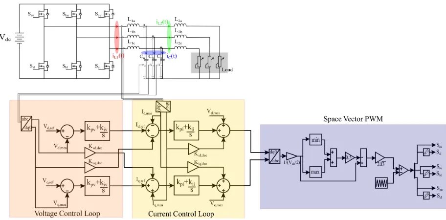
DQ PI control is also commonly used for voltage control of inverters. A typical
imple-mentation of dq voltage control is shown in Fig. 2.3. The control in Fig. 2.3 is composed
of an outer voltage loop and an inner current loop, and is referred to as multi-loop
volt-age control. The voltvolt-age control also includes virtual impedance, where the voltvolt-age drop
across a virtual impedance is subtracted from the voltage reference. Virtual impedance
is discussed in more detail in Ch 4.
(b) Current Control Loop
DQ PI control is commonly used for current control in inverters. A typical
implemen-tation of dq0 current control is shown in Fig. 2.3, which includes output voltage
feed-forward and decoupling terms. Thedq0 frame aligns the q-axis with the grid voltage by
converting the grid voltage todq0, driving the d-axis voltage to zero with a PI controller,
and feeding the integral of the PI output back as the dq0 transformation angle.
By feeding-forward the output voltage and the inductor voltage drop coupling term,
the current controller can be made into a single-input-single-output transfer function,
Sau
Sal
Sbu
Sbl
Scu
Scl Vdc
L1a L2a
L1b L2b
L1c L2c
Ca CbCc
Figure 2.3: Three Phase Inverter Controller Block Diagram
and decoupling terms commonly used indq0 current control have been implemented in
this control as well.
The inverter control parameters have been adapted from a Three phase, 100kW Schneider
inverter available off the shelf.
Table 2.1: Three Phase Inverter-Model Parameters
Parameter Value
Inverter-side filter inductor (L1) 750µH
Filter capacitor (C) 70µF
Grid-side filter inductor (L2) 1.7mH
Voltage Controller (kpv,Z) 0.17
Voltage Controller (kiv,Z) -0.158
Current Controller (kpi,Z) 2.5
Current Controller (kii,Z) -2.46
Frequency Droop Gain (mp) -1/100000
3. PWM Modulation Scheme
Space Vector PWM Modulation have been used to increase the output voltage range of the
converter for a given input [21].
PWM Comparison
Duty Cycle -1.0
-0.8 -0.6 -0.4 -0.2 0.0 0.2 0.4 0.6 0.8 1.0
Time (s)
1.988 1.992 1.996 2.000 2.004 2.008 2.012 2.016
D
u
ty
(
d
) 0
0
0
Reference Signal Sa Sb Sc
Duty_a Duty_b Duty_c
Figure 2.4: PWM Switching Sequence
Simulation Results
Implementing the switching model in PLECS, the inverter is observed to be stable and dual
loop-voltage control is implemented to control the inverter output loop-voltage of each phase to be same as
the grid phase voltage., i.e., 277√2 in dq0 reference frame.
Since the inverter is rated for 100kW, simulation results for the corresponding current through
Standalone Inverter_Vout
time (s)
1.304 1.306 1.308 1.310 1.312 1.314 1.316 1.318 1.320 1.322 1.324 1.326 1.328 1.330
V o lt ag e (V ) -400 -350 -300 -250 -200 -150 -100 -50 0 50 100 150 200 250 300 350 400 Vinv_a Vinv_b Vinv_c
Figure 2.5: 3-Phase Inverter Output Voltage Waveforms
StandaloneInverter_Iout
time (s)
1.080 1.082 1.084 1.086 1.088 1.090 1.092 1.094 1.096 1.098 1.100 1.102 1.104 1.106
C u rr en t (A ) -200 -180 -160 -140 -120 -100 -80 -60 -40 -20 0 20 40 60 80 100 120 140 160 180 200 Iinv_a Iinv_b Iinv_c
Standalone Inverter_Vout
time (s)
1.990 1.995 2.000 2.005 2.010 2.015 2.020 2.025 2.030
V o lt ag e (V ) -400 -350 -300 -250 -200 -150 -100 -50 0 50 100 150 200 250 300 350 400 Vinv_a Vinv_b Vinv_c
Figure 2.7: Three Phase Inverter Voltage Waveform during Load Change
StandaloneInverter_Iout
time (s)
1.990 1.995 2.000 2.005 2.010 2.015 2.020 2.025 2.030 2.035
C u rr en t (A ) -200 -180 -160 -140 -120 -100 -80 -60 -40 -20 0 20 40 60 80 100 120 140 160 180 200 Iinv_a Iinv_b Iinv_c
To check the controller bandwidth, the inverter’s response to a step change in load from 50kW
to 100kW can be seen in Fig. 2.7 and Fig. 2.8 and the results show that the controller bandwidth
is high-enough.
2.1.3 DC/DC Stage - Modeling
Distributed Energy Storage Devices(DESDs) are a very vital part of any kind of microgrids. During
an outage from the utility, the battery based energy storage device acts as a slack bus in the
microgrid and thus maintains the DC bus voltage in the system. Thus in a DC-DESD, the battery
bus is interfaced with a current controlled DC-DC converter.
S
1V
dc
Load
D
1L
dcC
dcV
dc
IsFigure 2.9: Boost Converter circuit diagram
The interfacing circuit between the battery and the DC-port of the 3-phase AC Storage Device
is basically a boost converterto step up the voltage level as required, the same is shown in Fig. 2.9.
To derive the transfer function of the converter,
1. Steady-state analysis
At steady-state, the volt-seconds of the inductor should be balanced and the charge balance
During ON State,
V
dc
Load
L
dcC
dcV
0
Is
Figure 2.10: Boost Converter - ON State
VL=L
diL
dt =Vbatt (2.25)
ic=C
dvcap
dt =−
Vcap
R (2.26)
During OFF State,
V
dc
Load
L
dcC
dcV
dc
IsFigure 2.11: Boost Converter - OFF State
VL=L
diL
dt =Vbatt−Vcap (2.27)
ic=C
dvcap
dt =IL−
Vcap
At steady state, for inductor Volt-Seconds (V.s) balance, LdiL
dt = 0
Thus,
D(Vbatt) + (1−D)(Vbatt−Vcap) = 0 (2.29)
This implies that,
Vcap=
Vbatt
1−D (2.30)
At steady-state, for capacitor-charge (q.C) balance, Cdvcap
dt = 0
Thus,
D(Vcap
R ) + (1−D)(IL− Vcap
R ) = 0 (2.31)
This implies that,
IL=
Vcap
(1−D)R (2.32)
2. Small-signal analysis
Perturbing a small value for each time varying parameter:
˜
vL=VL+L
dˆiL
dt (2.33)
˜ic=Ic+Ldˆvcap
dt (2.34)
˜
vbatt =Vbatt+ ˆvbatt (2.35)
˜
vcap=Vcap+ ˆvcap (2.36)
˜
d=D+ ˆd (2.37)
˜
The small signal analysis can be performed as follows: From volt-seconds balance:
˜
vL= ˜vbattd˜+ (˜vbatt−˜vcap) ˜d 0
(2.39)
cz Considering only the transient AC components,
LdˆiL
dt = ˆvbatt+Vcap ˆ
d−ˆvcapD 0
(2.40)
In Laplace domain,
sLˆiL(s) + ˆvcap(s)D 0
= ˆvbatt(s) +Vcapdˆ(s) (2.41)
From capacitor-charge balance:
˜ic=−v˜cap
R d˜+ (˜iL− ˜ vcap
R ) ˜d
0
(2.42)
Considering only the transient AC components,
Cdvˆcap
dt =−
ˆ vcap
R +Vcapdˆ−ILdˆ+ ˆiLD
0
(2.43)
In Laplace domain,
(sC+ 1
R)ˆvcap(s) = (1−D)ˆiL(s)−IL ˆ
d(s) (2.44)
From (2.41) and (2.44); defining the system in matrix form,
sL D0
D0 −(sC+R1)
ˆiL(s)
ˆ vcap(s)
= Vcap IL ˆ
d(s) +
1 0
vˆbatt(s)
Thus, the transfer function of the inductor current with respect to the duty variable can be
Gid =
ˆiL(s) ˆ d(s) =
(cVcap)s+ 2D 0
IL
LCs2+L
Rs+ (D
0
)2 (2.45)
Transfer function of output voltage with respect to the inductor current can be derived as,
Gvi =
ˆ vcap(s)
ˆiL(s) =
D0Vcap−(LIL)s
(CVcap)s+ 2D 0
IL
(2.46)
Transfer function of the output voltage with respect to the duty cycle can be derived as,
Gvd =
ˆ vcap(s)
ˆ
d(s) =
D0Vcap−(LIL)s
LCs2+ L
Rs+ (D
0
)2 (2.47)
Four switches have been used in the designed energy storage system along with the source
in-ductor split into two halves that make the system an ”Interleaved Bi-directional DC-DC converter”
as shown in Fig. 2.12
Vbatt
S
audc
S
aldc
S
budc
S
bldc
L adc
L bdc
Controller Design - Dual Loop Control
A boost converter can be controlled for it’s output capacitor voltage or it’s input inductor current.
Dual loop control is implemented for the current application, the outer voltage loop would maintain
the DC bus in the DESD at 400V and the inner interleaved current loops will maintain the current
through each inductor in each leg of the DESD depending on the load requirement.
1. Current Loop
Thus, considering (2.46) for the transfer function of inductor current to voltage, and since
all parameters are DC, using a PI controller should help control the current in a current
controlled boost converter.
The transfer function of the PI controller can be realized as,
Gci=Kpi+
Kii
s (2.48)
Magnitude (dB)
-20 -10 0 10 20 30 40 50 60
100 101 102 103 104 105
Phase (
deg)
-135 -90 -45 0 45 90
Current Controller Bandwidth (DC DESD) Gm = Inf , Pm = 85 deg (at 1.45e+04 rad/s)
Frequency (rad/s)
So the loop gain can be realized as,
GLGi =GidGci (2.49)
From MATLAB, the values of Kp and Ki can be derived and the bode plot of the loop gain
GLGi is as shown in Fig. 2.13,
2. Voltage Loop
A PI controller is used to control theDC bus voltage. Since the DESD is bi-directional, the controller bandwidth is modeled such that it can operate both in buck and boost mode at
the commanded DC bus voltage. The voltage loop bandwidth can be seen from the bode-plot
of the loopgain GLGv below,
Gcv =Kpv+
Kiv
s (2.50)
Magnitude (dB)
-100 -80 -60 -40 -20 0 20 40 60 80 100
100 101 102 103 104 105 106 107
Phase (
deg)
90 135 180 225 270 315
Voltage Controller Bandwidth (DC DESD)
Gm = 39.6 dB (at 6.38e+04 rad/s) , Pm = 91.8 deg (at 2.95e+03 rad/s)
Frequency (rad/s)
Since this is the outer loop to the current controller loop, the voltage controller loop gain would
be as follows and the bode-plot to show the voltage-controller bandwidth can be observed in
Fig. 2.14
GLGv = (
GLGi
1 +GLGi
Gvi)Gcv (2.51)
Vbatt
S
audc
S
aldc
S
budc
S
bldc Ladc
Lbdc
Figure 2.15: DC-DESD control loop simulation block diagram
Simulation Results
Bipolar modulation is used for the Pulse Width Modulation (PWM) to generate the gate
pulses to all four switches. Due to the interleaved design, the triangular waves used for the
modulation in each interleaved controller leg are aligned 180◦ apart as shown in Fig. 2.15
For a load change from 1.25kW to 5kW, using the controller parameters defined in Table.
2.2, the inductor currents on the input side for the interleaved operation can be observed to
Inductor Currents
Time (s)
1.20 1.25 1.30 1.35 1.40 1.45 1.50 1.55 1.60 1.65 1.70 1.75
C u rr en t (A ) 2 4 6 8 10 12 14 16 18 20 22 24 26 28 30 Ind. Current_a Ind. Current_b Inductor Currents Time (s)
1.568014 1.568018 1.568022 1.568026 1.568030 1.568034 1.568038 1.568042 1.568046
C u r r e n t ( A ) 16.5 17.0 17.5 18.0 18.5 19.0 19.5 20.0 20.5 21.0 21.5 22.0 22.5 23.0 23.5 24.0 24.5 25.0
25.5 Ind. Current_a
Ind. Current_b
Figure 2.16: DC DESD inductor current waveforms: (a)Step response of inductor currents, (b)DC-DESD inductor current ripple in each interleaved phase
The inductor current ripple on the input side is shown in Fig. 2.16, The peak-to-peak ripple
of each inductor is around 9A at full-load, i.e., around 40% of full-load average current in
each inductor.
Source Current (I_batt)
Time (s)
2.509480 2.509490 2.509500 2.509510 2.509520 2.509530
C ur re nt ( A ) 29 30 31 32 33 34 35 36 37 38 39 40 41 42 43 44 45 46 47 48 49 50 51 52 53 54
55 Source current
Figure 2.17: DC DESD battery current ripple
Table 2.2: Interleaved DC/DC Boost Converter-Model Parameters
Parameter Value
Battery-side inductor (L1 and L2) 120µH
Battery-side capacitor (Cbatt) 22µF
DC bus-side capacitor (CDC) 60µH
Voltage Controller (kpv) 0.6299
Voltage Controller (kiv) 70.8
Current Controller (kpi) 4.054×10⁻³
Current Controller (kii) 6.6856
profile of the batteries. The peak-to-peak current ripple here is around 3A at full-load, i.e.,
around 7% of full-load current. Thus, the current is much smoother here providing a much
better charging and discharging transient, Fig. 2.17 shows the simulation result for the same.
2.1.4 Battery Interface
There are basically three types of battery models reported in the literature, specifically:
experi-mental, electrochemical and electric circuit-based. Experimental and electrochemical models are
not well suited to represent cell dynamics for the purpose of state-of-charge (SOC) estimations of
battery packs [22]. Electric circuit-based models can be useful to represent electrical characteristics
of batteries. The most simple electric model consists of an ideal voltage source in series with an
internal resistance. The open circuit voltageVOC gives the voltage across the ideal battery, whereas
the voltage across the ideal battery and resistance Rb gives the terminal voltage of the batteryVb.
The true internal resistance of the battery is highly related to the State-Of-Charge (SOC) and
the electrolyte concentration of the battery bank. To take recognition of the role of the state of
charge, this battery model varies the resistance of the battery, i.e. Rb is a function of the state of
charge (SOC). This model assumes the same characteristics for the charge and the discharge cycles.
The open voltage source is calculated with a non-linear equation based on the actual SOC of the
battery [5]. The controlled voltage source is described by,
VOC =VOC0−K
Q
Q−R
idt +Ae
−BR
VOC=f(Ibatt,t)
Internal Resistance
Rb
Ibatt
VOC Controlled
Voltage Science
Vbatt
Figure 2.18: Battery Model Circuit Diagram [5]
Vbatt=VOC −RbIbatt (2.53)
whereVOC is the no load battery voltage (V),Kis the polarization voltage (V),Qis the battery
capacity (Ah), A is the exponential zone amplitude (V), B is the exponential zone time constant
inverse (Ah−1), Vbatt is the battery voltage (V), Rb is the battery internal resistance (Ω), Ibatt is
the battery current (A), and R
idt is the charge supplied and drawn by the battery (Ah).
The model has a non-linear term equal to KQ−QR
idt. This term represents a non-linear voltage
that changes with the amplitude of the current and the actual charge of the battery. So when the
battery is almost completely discharged and no current is flowing, the battery voltage increases
to nearly E0. As soon as a current circulates again, the voltage falls abruptly. This behaviour is representative of a real battery.
2.2
Inverter based Distributed Generator Emulation
Most of the DC distributed sources connecting to a three-phase AC line would need a similar power
electronic interface with a three-phase inverter in cascade. Thus, more DERs can be emulated in
the current system at test by connecting more such inverters in parallel. Thus, the overall system
lot of research is going on in this regard [23, 24, 25, 26] but that is beyond the scope of this thesis.
2.3
Synchronous Generator Model
Synchronous machines are AC machines that have a field circuit supplied by an external DC source.
In a synchronous generator, a DC current is applied to the rotor winding producing a rotor magnetic
field. The rotor is then turned by external means producing a rotating magnetic field, which induces
a 3-phase voltage within the stator winding. Field windings on rotor produce the main magnetic
field and the voltage is induced in the armature windings of stator.
The rotor of a synchronous machine is a large electromagnet. The magnetic poles can be either
salient or non-salient construction.
2.3.1 Modeling
By definition, in synchronous generators, the frequency of the electricity produced by synchronous
generators is synchronized with the mechanical rotational speed.
For a 4-pole machine, since the electrical frequency for the system is 60Hz, the synchronous
speed of the generator can be calculated as,
Nm=
120∗fe
p (2.54)
Thus, the synchronous speed of the machine is 1800rpm.
2.3.2 Control
This research is focused on residential microgrids and thus, the synchronous generators under
con-sideration are in the range of hundreds of kW. Thus the controller is mainly based on modern
electronic governor and automatic voltage regulator (AVR) control systems used for internal
com-bustion engine driven generators. The basic control diagram for a synchronous generator is as
Figure 2.19: Synchronous Generator Block Diagram, Adapted from [1]
1. Governor
The governor measures the shaft speed and adjusts the engine throttle position to regulate the
speed to the desired set point. Following figure shows the basic model for the diesel engine and
governor. The reference speed command comes from the corresponding real-power command
through the power sharing loop using a P-f droop curve or from an automatic generator
control (AGC). The simplified governor control is emulated through a PID control, and the
diesel engine is modeled as an actuator time constant and time delay [1]. The output of the
PID controller sets the torque command on the generator mechanical shaft.
The available synchronous generator model in PLECS library is used with the parameters
in Table. 2.4. For a 100kVA standalone synchronous generator with an RC load, since the
frequency is maintained at the nominal value (the P-f droop curve is defined as the same for
the inverter), the speed of the machine is always maintained at 1800rpm.
Fig. 2.21 shows the controller response to a load change from 50kW to 100kW. It can be
w
mw
refPI
control
1
1+sT
1e
-sT2T
mT
Lw
m1
B+sH
Figure 2.20: Governor Control Circuit Block Diagram
P_offset from nominal (100kW)
Frequency Reference- From Droop curve (f_ref)
Speed Reference (w_ref)
Measured Speed (w_mea) × 1e5 P o w er ( W ) -1.0 -0.5 0.0 F re q u en c… 60.0 60.5 61.0 S p ee d ( rp m ) 1800 1810 1820 1830 Time (s)
0 2 4 6 8 10 12 14 16 18
S p ee d ( rp m ) 0 1000 2000 P_error f_ref w_ref w_mea
is maintained at the corresponding frequencies according to the Active Power-Frequency droop
curve.
2. Automatic Voltage Regulator (AVR)
The DC excitation system for the synchronous generator that controls the terminal voltage
comprises of an Automatic Voltage Regulator (AVR) and a brushless exciter. The AVR gets
a reference command for terminal voltage through a power-system stabilizer or a Q-V droop
curve with respect to voltage. Using a simplified PID control to emulate the modern digital
AVRs [1], the exciter is supplied to, through a power amplifier. The simplified brushless exciter
here is emulated using a simple first order-transfer function with a time constant,TE and an
exciter gain,KE.
V
rmsV
refPID
control
1
1+sT
3Amplifier
1
sT
EK
ES
EFigure 2.22: AVR Control Circuit Block Diagram
For the generator parameters shown in Table. 2.4, Fig. 2.23 shows the controller response to a
load change from 50kW to 100kW. It can be observed that the transient during the dynamic
load change is small and the generator’s terminal voltage is maintained at the corresponding
value according to the Reactive Power-Voltage droop curve. The nominal voltage i.e., 240VL−L
From the figure above, the reactive power of 4kVA generated in the system is due to the
capacitive load and since the slope of the droop curve is very small, the deviation in the terminal
voltage from nominal value is very low. Thus, the generator can maintain the terminal voltage close
to 240VL−Lat any load condition.
From Table. 2.3, the PID controller gains in the governor for the 100kVA generator in the current
application are chosen such that the commanded power sharing is met at the corresponding rotor
speed. Similarly, to maintain the terminal voltage, proper gains in AVR are chosen corresponding
to the reactive power sharing. These controller gains are adapted from [1].
Table 2.3: 100kVA Synchronous Generator-Controller Parameters [1]
Parameter Value
AVR (kp) 1.62
AVR (ki) 10.4
AVR (kd) 0.05
AVR (Td) 0.1
AVR (TE) 0.01
AVR (KE) 1
AVR (SE) 0
Governor (kp) 7
Governor (ki) 57
Governor (kd) 0
Governor (Td) 0
Engine (T1) 0 s
Engine (T2) 0 s
The initial transient in the voltage and speed waveforms is due to the generator’s inertia. The
steady-state response of the generator terminal voltage and the generator phase currents as load
increases from 50kW to 100kW is shown in Fig. 2.24, The amplitude of generator phase currents
Q_offset from nominal (0kVA)
Terminal Voltage Reference- From Droop curve (Vt_ref)
Measured Terminal Voltage (Vt_mea)
Applied Field voltage (Vf)
P o w er ( V A ) -8000 -6000 -4000 -2000 0 V o lt ag e (V ) 138.56 138.57 138.58 138.59 V o lt ag e (V ) 0 100 200 Time (s)
0 2 4 6 8 10 12 14 16 18
V o lt ag e (V ) 0 200 400 600 Q_error Vt_ref Vt_mea Vf
Figure 2.23: AVR following the Voltage Reference and applying the corresponding Vf
Generator Terminal Voltage (Vt)
Time (s)
9.635 9.640 9.645 9.650 9.655 9.660 9.665 9.670 9.675 9.680 9.685 9.690 9.695 9.700
V o lt a g e ( V ) -340 -320 -300 -280 -260 -240 -220 -200 -180 -160 -140 -120 -100-80 -60 -40 -200 20 40 60 80 100 120 140 160 180 200 220 240 260 280 300 320 340 V_terminal
Phasor Currents_Sync Gen (I_abc)
Time (s)
9.650 9.654 9.658 9.662 9.666 9.670 9.674 9.678 9.682 9.686
C u r r e n t ( A ) -340 -320 -300 -280 -260 -240 -220 -200 -180 -160 -140 -120 -100-80 -60 -40 -200 20 40 60 80 100 120 140 160 180 200 220 240 260 280 300 320 340 Ia_SG Ib_SG Ic_SG
Table 2.4: 100kVA Synchronous Generator-Model Parameters
Parameter Value
Stator Resistance (Rs) 0.0166Ω
Stator Leakage Inductance (Lls) 148.014µH
Unsat. Magn. Inductance-d (Lmd0) 2.922mH Unsat. Magn. Inductance-q (Lmq0) 1.382mH Saturated Magn. Inductance-d (Lmdsat) 2mH
Saturated Magn. Inductance-d (Lmqsat) 2.922mH
Saturating Magnetizing flux (PsiT) 1
Field Resistance (R0f) 1.3Ω Field Leakage Inductance (L0lf) 124.247µH
Damper resistance-d (R0kd) 0.00237Ω
Damper resistance-q (R0kq) 0.0025Ω
Damper leakage inductance-d (L0lkd) 140.322µH Damper leakage inductance-q (L0lkq) 179.315µH
Inertia (J) 0.1
Friction Co-efficient (F) 0
Number of pole-pairs (p) 2
2.3.3 Permanent Magnet SG Vs. Wound Field SG
In a Permanent Magnet Synchronous Generator (PMSG), the reactive power cannot be controlled
since the rotor is a permanent magnet and thus, no external DC field excitation is required. Since
the terminal voltage of the generator cannot be regulated in a PMSG, the fault response we see in
this case might not justify the system stability in terms of fault-tolerance. But in a full Synchronous
generator, the real and reactive power are always controlled and thus, the actual power sharing
and impacts on each of the sources can be seen well. Thus, for the current purpose of testing fault
Chapter 3
Component Interactions in
Three-Phase Microgrids
After modeling all the three different types of DERs in Ch 2, they are interconnected and connected
to the superimposed power grid with loads, to study the interactions between them. Any component
may be connected and fed directly into any other component. The energy of the battery storage can
be fed to both the load and the host network, and from the superimposed grid, in turn, the charging
of the storage is possible. Furthermore, the load can be fed directly from the host network. From
this general fully-interconnected model, a specific model can be derived, required for the simulation
of the real microgrid. It is also necessary to incorporate technical or regulatory constraints that
may limit the flow of energy.
3.1
System at Test
The system under consideration in this thesis is a simplified inverter and generator based microgrid
model (Fig. 3.1) to demonstrate the interactions between each other when connected. The impact
on overall system stability is also discussed to an extent when multiple generators are tied together.
this work is as follows,
SG IM Drive
Load 277V 3ph Grid
Diesel Engine Emulator
Sync Gen.
240V 3ph
Figure 3.1: Microgrid System under test
3.2
Paralleled Inverter System
The growing penetration of power-electronic-based renewable energy sources into the modern power
system, such as solar and wind energy, efficiently reduces the total consumption of the fossil fuels.
Thus, renewable energy power plants are becoming a main conversion scheme to accomplish the
green and clean electricity generation. For these applications, grid-tied inverters are extensively
employed as flexible and efficient grid interfaces to connect the renewables to the grid [27]
Inverters connecting DC power supplies to AC systems occur in numerous applications.
Pho-tovoltaic power plants and battery storage installations are examples of such applications. Since
many such distributed generators needs to be tied together with an inverter interface in a real-world
implementation of microgrids, the stability and control of paralleled inverters become a crucial case
3.2.1 Operation
Although inverter topologies used for power transmission have traditionally been current sourced, in
recent years, voltage source inverters (VSI) have been increasingly used for high-power applications
like electric traction and mill drives, PV power systems and battery storage systems. Control scheme
for VSI used in this research have been explained in detail in Ch 3.
Figure 3.2: Parallel voltage sources concept illustration, Adapted from [6]
It is well known that stable operation of a power system needs good control of the real power
flow, P and the reactive power flow, Q. Thus, when multiple sources are tied together in a microgrid,
power sharing between the sources is of high-priority. Traditionally, the communication link between
all the inverters connected together sends the corresponding power dispatch command to each
inverter to maintain the load. Recent advancements in control of Uninterrupted Power supply (UPS)
systems make possible, their independent parallel operation, avoiding communication links between
the units. The advantages of such power configuration include high reliability and no restriction on
the physical location of the UPS units [28]. To achieve this special kind of parallel operation, the
droop method is often adopted. The droop method is based on a well-known concept in large-scale
power systems that consists of drooping the frequency of the ac-generator when its output power
increases. Control of a distributed system without communication can only be achieved at the price
of permitting a small error. The small droop is generally considered acceptable as long as the error
Usually, the inverter output impedance is assumed to be inductive due to both the high-inductive
component of the line-impedance and the large inductor of the output filter [6]. Based on this
as-sumption, the relation between real and reactive power to frequency and output voltage magnitude
respectively, can be determined as follows,
P = U1
R2+X2[R(U1−U2cosδ) +XU2sinδ] (3.1)
Q= U1
R2+X2[−RU2sinδ+X(U1−U2cosδ)] (3.2)
So for overhead lines, sinceX R,Rcan be neglected. Assuming the power angleδto be small,
sinδ =δ and cosδ= 1.
Thus, above equations become,
P ∼= U1U2
X δ (3.3)
Q∼= U1(U1−U2)
X (3.4)
Thus, for an inductive system, the power angle depends predominantly on P, whereas the
voltage difference depends predominantly on Q.
Real Power
Frequency
Reactive Power
V
oltage
Qmin Q0 Qmax
Vmax
Vmin
V0 mq
Pmin P0 Pmax
fmax
fmin
f0 mp
Thus, the frequency and voltage droop curve for the inverter can be determined as,
f−f0=−kp(P −P0) (3.5)
U1−U0 =−kq(Q−Q0) (3.6)
f0 and U0 are rated frequency and grid voltage respectively, and P0 and Q0 are the momentary
set points for active and reactive power of the inverter. The frequency and voltage droop control
characteristics are shown graphically in Fig. 3.3
Inverter Voltages (Paralleled)
Time (s)
1.108 1.110 1.112 1.114 1.116 1.118 1.120 1.122 1.124 1.126 1.128 1.130 1.132 1.134
V
o
lt
ag
e
(V
)
-280 -260 -240 -220 -200 -180 -160 -140 -120 -100 -80 -60 -40 -20 0 20 40 60 80 100 120 140 160 180 200 220 240 260 280
I II
Vinv1_a Vinv1_b Vinv1_c Vinv2_a Vinv2_b Vinv2_c
Figure 3.4: Three Phase paralelled inverter voltages at PCC
Droop control loop gives the system frequency reference from the generated real power (P) and
the inverter output voltage magnitude from the reactive power (Q) generated in the system. When
droop control is included to generate the voltage reference to the inverter controller, the power
sharing can be observed depending on the corresponding droop curves. To prove the concept, the
![Figure 1.1:Microgrid, Adapted from [3]](https://thumb-us.123doks.com/thumbv2/123dok_us/1523633.1186753/16.612.133.506.67.275/figure-microgrid-adapted-from.webp)
![Figure 1.2:Voltage Interconnection and Ride Through requirements, Adapted from [4]](https://thumb-us.123doks.com/thumbv2/123dok_us/1523633.1186753/18.612.116.501.73.354/figure-voltage-interconnection-ride-requirements-adapted.webp)
![Figure 1.3:Frequency Interconnection and Ride Through requirements, Adapted from [4]](https://thumb-us.123doks.com/thumbv2/123dok_us/1523633.1186753/19.612.115.500.143.323/figure-frequency-interconnection-ride-requirements-adapted.webp)