Probability-Driven Multi Bit Flip-Flop Design Optimization
with Clock Gating
Annem Siva
& Bommireddy Ajantareddy
[email protected] & [email protected]
1PG Scholar, VLSI, Krishnachaitanya institute of technology and sciences, Markapur. 2Assistant Professor, Department of ECE, Krishnachaitanya institute of technology and sciences,
Markapur.
Abstract: Data-Driven Clock-Gating (DDCG) and Multi Bit Flip-Flops (MBFFs) in which several FFs are grouped and share a common clock driver are two effective low power design techniques. Though commonly used by VLSI designers, those are usually separately treated. Past works focused on MBFF usage in RTL, gate-level and their layout. Though collectively coving the common design stages, the study of each aspect individually led to conflicts and contradiction with the others. MBFF internal circuit design, its multiplicity and its synergy to the FFs data toggling probabilities have not been studied so far. This work attempts to maximize the energy savings by proposing a DDCG and MBFF combined algorithm, based on Flip-Flops (FFs) data to-clock toggling ratio. It is shown that to maximize the power savings, the FFs should be grouped in MBFFs in increasing order of their activities. A power savings model utilizing MBFF multiplicities and FF toggling probabilities is developed, which was then used by the algorithm in a practical design flow. Simulation and synthesis reports are observed using Xilinx ISE design Suite, which shows much power savings in proposed when compared with traditional.
Keywords: Clock gating (CG), clock network synthesis, low-power design, multi-bit flip-flop (MBFF).
I.INTRODUCTION
A recently published paper has emphasized the usage of Multi-Bit Flip-Flops (MBFFs) as a design technique delivering considerable power reduction of digital systems. The data of digital systems is usually stored in Flip-Flops (FFs), each having its own internal clock driver. Shown in Fig. 1.1, an edge-triggered 1-bit FF contains two cascaded master and slave latches, driven by opposite clocks CLK and CLK. It is shown that most of the FF’s energy is consumed by
its
internal clock drivers, which are significant
contributors to the total power consumption.
The data of digital systems are usually stored in flip-flops (FFs), each of which has its own internal clock driver. In an attempt to reduce the clock power, several FFs can be grouped into a module called a multi-bit FF (MBFF) that houses the clock drivers of all the underlying FFs. We denote the grouping of k FFs into an MBFF by a k-MBFF. Kapoor et al.[1] Traditionally, digital control of SMPS was accomplished by applying a general purpose Digital Signal Processor (DSP). Apart from some limited applications, this approach is unsuitable in most industrial instances due to its many drawbacks and limitations. These include: the single arithmetic unit that limits the speed of computation resulting in a limited control bandwidth, excessive delays in a multi converter case, limited capabilities to generate non-sequential pulse as might be needed in non linear control, limited capabilities to achieve high resolution of the output driving signal and its degrading as the number of control channels increases, as well as other shortcomings.
remedy this, the MBFF internal drivers can be strengthened at the cost of some extra power. It is therefore recommended to apply the MBFF at the RTL design level to avoid the timing closure hurdles caused by the introduction of the MBFF at the backend design stage. Due to the fact that the average data-to-clock toggling ratio of FFs is very small, which usually ranges from 0.01 to 0.1. Clock gating does not come for free. Extra logic and interconnects are required to generate the clock enabling signals and the resulting area and power overheads must be considered. In the extreme case, each clock input of a FF can be disabled individually, yielding maximum clock suppression. This, however, results in a high overhead; thus suggesting the grouping of several FFs to share a common clock disabling circuit in an attempt to reduce the overhead. On the other hand, such grouping may lower the disabling effectiveness since the clock will be disabled only during time periods when the inputs to all the FFs in a group do not change. In the worst case, when the FFs’ inputs are statistically independent, the clock disabling probability equals the product of the individual probabilities, which rapidly approaches zero when the number of involved FFs increases. It is therefore beneficial to group FFs whose switching activities are highly correlated and derive a joint enabling signal.
In an attempt to reduce the clock power, several FFs can be grouped in a module such that common clock drivers are shared for all the FFs. Two 1-bit FFs grouped into 2-bit MBFF, called also dual-bit FF, is shown in Fig. 1. In a similar manner, grouping of FFs in 4-bit and 8-bit MBFFs are possible too. We subsequently denote a k -bit MBFF by k -MBFF. MBFF is not only reducing the gate capacitance driven by a clock tree. The wiring capacitive load is also reduced because only a single clock wire is required for multiple FFs. It also reduces the depth and the buffer sizes of the clock tree and also the number of sub-trees. Beyond clock power savings those features also reduce the silicon area.
Fig. 1.1.1-bit FF and 2-MBFF.
II. LITERATURE SURVEY
Digital Systems Power Management for High Performance Mixed Signal Platforms
High performance mixed signal (HPMS) platforms require stringent overall system and subsystem performance. The ability to design ultra-low power systems is used in a wide range of platforms including consumer, mobile, identification, healthcare products and microcontrollers. In this paper we present an overview of low power design techniques, challenges and opportunities faced in an industrial research environment. It presents strategies on the deployment of low power techniques that span from power-performance optimization scenarios accounting for active and standby operation modes to the development of multi-core architectures suitable for low voltage operation. [1]
The Optimal Fan-Out of Clock Network for Power Minimization by Adaptive Gating
graphics processor and a 16-bit microcontroller, both designed at 65-nanometer technology. [2]
III. Data Driven Clock Gating for single Flip-flop
Data driven gating is causing area and power overheads that must be considered. In an attempt to reduce the overhead, it is proposed to group several FFs to be driven by the same clock signal, generated by bring the enabling signals of the individual FFs. This may however, lower the disabling effectiveness. It is therefore beneficial to group FFs whose switching activities are highly correlated and derive a joint enabling signal. In a recent paper, a model for data driven gating is developed based on the toggling activity of the constituent FFs. The optimal fan-out of a clock gate yielding maximal power savings is derived based on the average toggling statistics of the individual FFs, process technology, and cell library in use. In general, the state transitions of FFs in digital systems depend on the data they process. Assessing the effectiveness of data-driven clock gating requires, therefore, extensive simulations and statistical analysis of the FFs’ activity.
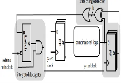
The dynamic power consumption could be reduced by using clock gating technique. This data driven clock gating signals having toggling activity to enable the clock signals. So the flip-flops and the latches are to be enabled by using the gate signals. The outputs from the X-OR gates are OR end to give the combination of output joint gate signals from the flip-flops and then latched to avoid the glitches presented in the specified units.
Fig 2 Clock Gating using for single Flip-flop.
I. Introducing clock-gating into MBFF Let p be the data-to-clock toggling probability. Denote by E1 the expected energy consumed by 1-bit FF.
E1 (P) =λ1+µ1p…….. (1)
where 1 is the energy of the FF’s internal clock driver, and 1 is the energy of data toggling. For 2-MBFF there are three possible scenarios: none of the FFs toggle, a single FF toggles, and both FFs toggle. Assuming data toggling independence, the expected energy consumption E2 is
E2 (p) = (1-p) 2+2(λ2+µ2) p (1-p) + (λ2+2µ2) p2=λ2+2µ2
… (2)
Where 2 is the energy of the internal clock driver, and 2 is the per-bit data toggling energy. For the general case of k -MBFF, let k be the energy of the MBFF’s internal clock driver and k be the per-bit data toggling energy. Considering all the combinations of toggling FFs, the expected energy is
EK(p)=∑j=0k(λk+jµk)(kj) p j(1-p)kj=λk+kµk…(3)
The equality in (3) is obtained by applying some rearrangements.
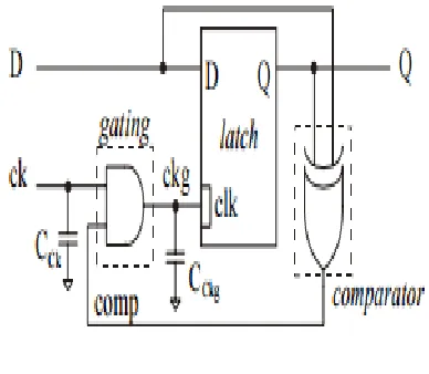
The MBFFs discussed so far were driven by a free-running un-gated clock signal. Fig. 4.1 illustrates a DDCG integrated into a k -MBFF. All the shaded circuits reside within a library cell. It was shown in [2] that given an activity p, the group size k which maximizes the energy savings solves the equation.
(1-p)k ln (1-p) CFF +Clatch/K2=0 …(4) where CFF and Clatch are the clock input loads of a FF
Fig 3: DDCG integrated into k -MBFF.
P 0.01 0.02 0.05 0.1
K 8 6 4 3
Table 1 : Dependency of the optimal MBFF multiplicity on toggling probability.
Unless otherwise stated the MBFFs discussed in the sequel are DDCG. To grasp the power savings achievable by DDCG of a k -MBFF, Fig. 3 has been simulated with SPICE for various activities p and multiplicities 2,4,8 . The powerk consumption of a 2-MBFF. Line (a) represents the power consumed by two 1-bit FFs driven independently of each other. The
3.8 W power consumed for zero activity is due to the toggling of the clock driver at each FF, and it is always being consumed regardless of the activity. Line (b) corresponds to the ideal case where the two FFs toggle simultaneously. In that case the clock driver shared by the two FFs either toggles for the sake of the two, or it is disabled by the internal gater shown in Fig. 3. Expectedly, the power consumed for zero activity is nearly half compared to two 1-bit FFs. As the activity increases, the power of (b) is growing faster than (a) since the gating circuit consumes power proportionally to the activity.
There is no point in using a 2-MBFF beyond the 0.17 activity crossing point, a case where power starts being lost.
Fig 4: Power consumption of 2 FFs vs. 2-MBFF.
Line (c) shows the case where the FFs are toggling disjoint. This is obviously the worst case since the clock driver works for the two FFs, while only one needs it. As for (b), in case of disjoint toggling there is no point in using 2-MBFF if the FFs activities are higher than 0.11. Given an activity, the power savings of 2-MBFF is the distance between line (b) or (c) to (a). Notice that for zero activity the per-bit power savings is (3.8- 1.8)/2=1.0w.
FFs should be grouped in a DDCG MBFF.
probability-driven FFs grouping. The analysis so far assumed that all the FFs grouped in a MBFF have same data toggling probability p. FFs’ toggling probabilities are usually different of each other, and an important question is therefore how the probability varieties affect the FFs grouping. Past works considered either structural FFs grouping (e.g., successive bits in registers), or post-layout grouping driven by physical proximity. We subsequently show that data toggling probabilities matter and should be considered for maximizing energy savings.
Given n FFs 1 FF n i i , consider their grouping in 2-MBFFs. Let a 2-MBFF, denoted , FFi j , comprise FFi and FFj , toggling independently with probabilities i p and j p , respectively. When none is toggling, the clock of , FFi j is disabled and its internal 10 clock driver does not consume dynamic energy. When both FFi and FFj are toggling, the clock of , FFi j is enabled and the clock driver energy is fully useful and there is no waste. A waste happens when one FF is toggling, while its counterpart does not. There, the clock pulse is enabled, driving both FFs, whereas only one needs it. A waste i j , W of half of the internal clock driver energy 2 thus occurs (see (2)), given by
w(i,j) = 2/2[pj (1-pi)+pl(1-pj)= 2/2 (pi+pj-2
pipj)]….(5)
Given FFi , FFj , FFk and FFl , their pairing in two 2-MBFFs yields the energy waste
W (i, j) + w (k, l) =2/2[pi+pj+pk+pl-2(pipj+ pkpl)]
While the term (a) of (9) is independent of the pairing, the term (b) does depend. The expression i j k l , ,
W W is minimized when (b) is maximized. If , i j k l p p p
The pairing {FF(i,j), FF(k,l )} is favored over {FF(i,j),
FF(k,l )} since (w(i,j)+ w(k,l))–
(w (i,k)+ w(j,l)) = -2(pi-pl) (pj-pk)/2<0. {FF(i,j), FF(k,l )} is similarly favored
Over {FF(i,j), FF(k,l )} the generalization for pairing
of n FFS is straight forward
.
The generalization for pairing of n FFs is straight forward. Let n be even and 2 , 1 : FF n s t i i i P be a pairing of FF ,FF , ,FF 1 2 n in n 2 2-MBFFs. The following energy waste W P results in
W (p) = ∑i=1n/2w (si,ti) =2/2[∑j=1npj-2
∑i=1n/2psipti]…(8)
Since 1 n j j p is independent of the pairing, W P is minimized when 2 1 n s t i i i p p is maximized. The optimal pairing minimizing W P is defined by the following theorem [8].
Theorem 1. Let n be even and let FF ,FF , ,FF 1 2 n be ordered such that their toggling probabilities satisfy 1 2 n p p p . The pairing 2 2 1,2 1 : FF n i i i P of successive FFs is minimizing W P given in (10). The above result of grouping in 2-MBFFs is generalized for grouping in k -MBFFs as follows. 11 Theorem 2. Let n be divisible by k , and let FF ,FF , ,FF 1 2 n be ordered such that their toggling
probabilities satisfy 1 2 n p p p . The grouping of
P: {FF (k(i-1)+1,…,ki)}n/ki=1
Successive FFs is minimizing the energy waste incurred by the nk k -MBFFs. The case where n is not divisible by k has also been addressed.
V. RESULTS Simulation.
Technology Schematic.
Design Summary.
Logic
Utilization Used Available Utilization
Number of
slices 0 4656 0%
Number of bonded iobs
33 232 14%
Power Comparison Table.
SYSTEM POWER
EXISTING 0.84 Watt
PROPOSAL 0.081Watt
VI. CONCLUSION
Clock gating is used in fifo to reduce the power consumption. For further power saving data driven clock gating and multi-bit flip-flops are used in sequential circuits. Common clock gating is used for power saving. But clock gating still leaves larger amount of redundant clock pulses. Multi-bit flip-flop is also used to reduce power consumption. Using of Multi-bit Flip-Flop method is to eliminate the total inverter number by sharing the inverters in the flip-flops. Combination of Multi-bit Flip-Flop with Data driven clock gating will increase the further power saving. Xilinx software tool is used for implementing this proposed system. The combination of data-driven gating with MBFF in an attempt to yield further power savings.
REFERENCES
1. Kapoor, Ajay, Cas Groot, Gerard Villar Pique, Hamed Fatemi, Juan Echeverri, Leo Sevat, Maarten Vertregt et al. “Digital systems power management for high performance mixed signal platforms.” Circuits and Systems I: Regular Papers, IEEE Transactions on 61, no. 4 (2014): 961-975.
2. Wimer, Shmuel, and Israel Koren. “The optimal fan-out of clock network for power minimization by adaptive gating.” Very Large Scale Integration (VLSI) Systems, IEEE Transactions on 20, no. 10 (2012): 1772-1780.
3. Santos, Cristiano, Ricardo Reis, Guilherme Godoi, Marcos Barros, and Fabio Duarte. “Multi-bit flip-flop usage impact on physical synthesis.” In Integrated Circuits and Systems Design (SBCCI), 2012 25th Symposium on, pp. 1-6. IEEE, 2012.
4. Yan, Jin-Tai, and Zhi-Wei Chen. “Construction of constrained multi-bit flip-flops for clock power reduction.” In Green Circuits and Systems (ICGCS), 2010 International Conference on, pp. 675-678. IEEE, 2010. 15
5. Jiang, IH-R., Chih-Long Chang, and Yu-Ming Yang. “INTEGRA: Fast multibit flip-flop clustering for clock power saving.” Computer-Aided Design of Integrated Circuits and Systems, IEEE Transactions on 31, no. 2 (2012): 192-204.
Design of Integrated Circuits and Systems 32, no. 2 (2013): 242-246.
7. Lo, Shih-Chuan, Chih-Cheng Hsu, and Mark Po-Hung Lin. "Power optimization for clock network with clock gate cloning and flip-flop merging." In Proceedings of the 2014 on International symposium on physical design, pp. 77-84. ACM, 2014.
8. Wimer, Shmuel, Doron Gluzer and Uri Wimer. “Using well-solvable minimum cost exact covering for VLSI clock energy minimization.” Operations Research Letters 42, no. 5 (2014): 332-336.
9. Wimer, Shmuel, and Israel Koren. “Design flow for flip-flop grouping in datadriven clock gating.” Very Large Scale Integration (VLSI) Systems, IEEE Transactions on 22, no. 4 (2014): 771-778.
10. Wimer, Shmuel. “On optimal flip-flop grouping for VLSI power minimization.” Operations Research Letters 41, no. 5 (2013): 486-489.