Probability-Driven Multibit Flip-Flop Integration with
Clock Gating
B. Manasa Reddy, B. Jhansi Reddy
,
R. Sindhu Reddy
1 Assistant Professor, Dept of ECE, TKR College Of Engineering And Technology, Meerpet, Ranga Reddy, Telangana, India
Abstract: Data-Driven Clock-Gating (DDCG) and Multi Bit Flip-Flops (MBFFs) in which several FFs are grouped and share a common clock driver are two effective low power design techniques. Though commonly used by VLSI designers, those are usually separately treated. Past works focused on MBFF usage in RTL, gate-level and their layout. Though collectively coving the common design stages, the study of each aspect individually led to conflicts and contradiction with the others. MBFF internal circuit design, its multiplicity and its synergy to the FFs data toggling probabilities have not been studied so far. This work attempts to maximize the energy savings by proposing a DDCG and MBFF combined algorithm, based on Flip-Flops (FFs) data to-clock toggling ratio. It is shown that to maximize the power savings, the FFs should be grouped in MBFFs in increasing order of their activities. A power savings model utilizing MBFF multiplicities and FF toggling probabilities is developed, which was then used by the algorithm in a practical design flow. We achieved 17% to 23% power savings compared to designs with ordinary FFs.
Keywords: Clock gating (CG), clock network synthesis,
low-power design, multibit flip-flop (MBFF).
I.INTRODUCTION
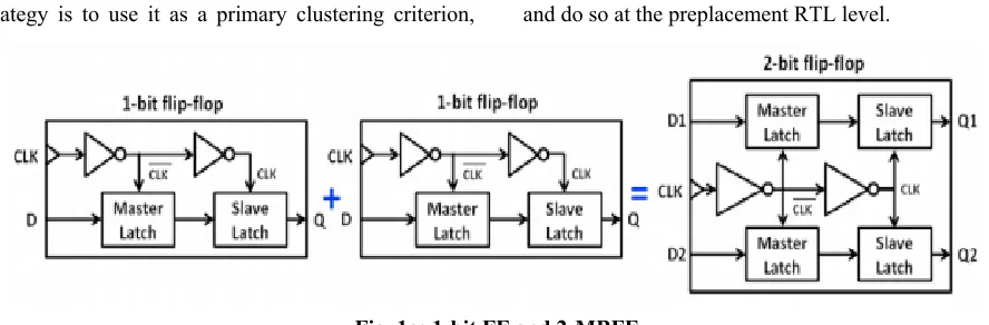
A recently published paper has emphasized the usage of Multi-Bit Flip-Flops (MBFFs) as a design technique delivering considerable power reduction of digital systems [1]. The data of digital systems is usually stored in Flip-Flops (FFs), each having its own internal clock driver. Shown in Fig. 1a, an edge-triggered 1-bit FF contains two cascaded master and slave latches, driven by opposite clocks CLK and CLK. It is shown in that most of the FF’s energy is consumed by its internal clock drivers, which are significant contributors to the total power consumption.
In an attempt to reduce the clock power, several FFs can be grouped in a module such that common clock drivers are shared for all the FFs. Two 1-bit FFs grouped into 2-bit MBFF, called also dual-bit FF [1], is shown in Fig. 1a. In a similar manner, grouping of FFs in 4-bit and 8-bit MBFFs are possible too. We subsequently denote a k -bit MBFF by k -MBFF. MBFF is not only reducing the gate capacitance driven by a clock tree. The wiring capacitive load is also reduced because only a single clock wire is required for multiple FFs. It also reduces the depth and the buffer sizes of the clock tree and also the number of sub-trees. Beyond clock power savings those features also reduce the silicon area.
Most distributed deals with MBFF have concentrated on physical execution, driven basically by the postplacement format [4], [5], [7], [8], [13], [16]. In these works, FF exercises have a tendency to be overlooked. Each FF is related with time edges got from the design including 1-bit FFs. The wires associated with the information and yield of a FF are secured on their contrary side to whatever is left of the rationale, though the position of the FF is permitted to move around without abusing timing. This characterizes the district in the design where the FF can be dislodged and converged into the MBFF. The 2-MBFF combining is defined as an advancement issue that goes for boosting the quantity of blended FFs.
strategy is to use it as a primary clustering criterion, and do so at the preplacement RTL level.
Fig. 1a: 1-bit FF and 2-MBFF.
The main contributions of this brief are as follows:
1) A design methodology that fuses MBFF and DDCG, yielding considerable power savings;
2) A probability driven algorithm that minimizes the expected DDCG MBFF power consumption.
Clock gating:
Several techniques to reduce the dynamic power have been developed, of which clock gating is predominant. Ordinarily, when a logic unit is clock, its underlying sequential elements receive the clock signal regardless of whether or not they will toggle in the next cycle. Clock enabling signals are usually introduced by designers during the system and clock design phases, where the inter-dependencies of the various functions are well understood.
In contrast, it is very difficult to define such signals in the gate level, especially in control logic, since the inter-dependencies among the states of various flipflops depend on automatically synthesized logic. There is a big gap between block disabling that is driven from the HDL definitions, and what can be achieved with data knowledge regarding the flip-flops activities and how they are correlated with each other. The research presents an approach to maximize clock disabling at the gate level, where the clock signal driving a flip-flop is disabled (gated) when the flip-flop states is not subject to a change in the next clock cycle. Figure.1b shows enabling of the clock signal.
On the other hand, such grouping may lower the disabling effectiveness, since the clock will disabled only when the inputs to all the flip-flops in a group don’t change. It is, therefore beneficial to group flip-flops whose switching activities are highly correlated in derive a joined enabling signal.
Fig.1b: Enabling of the clock signal
II. INTEGRATING CLOCK GATING INTO MBFF
Let p be the data-to-clock toggling probability. Denote by E1 the expected energy consumed by 1-bit FF.
For the general case of k -MBFF, let λk be the energy of the MBFF’s internal clock driver and µk be the per-bit data toggling energy. It is important to note that toggling independence is a pessimistic assumption. In reality, the correlation between FF toggling yields higher energy savings than the model in [2].
Fig. 2 illustrates a DDCG integrated into a k-MBFF. The shaded circuits reside within a library cell.
Fig.2: DDCG integrated into a k-MBFF
Given an activity p, the group size k that maximizes the energy savings solves the equation
where CFF and Clatch are the clock input loads of an FF and a latch, respectively [2]. The solution to (3) for various activities is shown in Table I for typical CFF and clatch. The above optimization does not take into account the clock driver sharing, which also affects the optimal grouping as shown below.
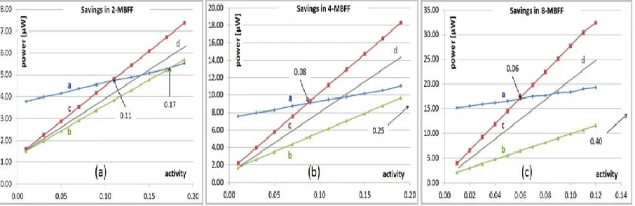
To grasp the power savings of a k-MBFF achievable by DDCG, Fig. 1 was simulated with SPICE for various activities p and k = 2, 4, 8. Fig. 3(a) shows the power consumption of a 2-MBFF. Line (a) is the power consumed by two 1-bit FFs driven independently of each other. The 3.8-μW power at zero activity is due to the toggling of the clock driver at each FF, and it is always consumed regardless of the activity.
Fig. 3: Power consumption of k 1-bit FFs compared to k-MBFF: 2-MBFF (a), 4-MBFF (b) and 8-MBFF (c). Line (a) is the power consumed by k 1-bit FFs driven independently of each other. Line (b) is the ideal case of
simultaneous (identical) toggling. Line (c) is the worst case of exclusive (disjoint) toggling. Line (d) is an example of realistic toggling.
Line (b) corresponds to the ideal case where the two FFs toggle simultaneously (identically). In this case, the clock driver shared by the two FFs either toggles for the sake of the two or is disabled by the internal gate shown in Fig. 2. As expected, the power consumed for zero activity is smaller than two 1-bit FFs. As the activity increases, the power of line (b) rises faster than that of line (a) since the gating circuit
overhead consumes power proportionally to the activity. There is no point in using a 2-MBFF beyond the 0.17 activity crossing point, the case where power starts to be lost.
one needs it. Similar to line (b), in exclusive toggling, there is no point in using the 2-MBFF if the FF activities are higher than 0.11.
For a given activity and toggling scenarios of line (b) or (c), the power saving of the 2-MBFF is their distance to line (a). Note that for zero activity, the per-bit power saving is (3.8 − 1.8)/2 = 1.0 μW. The interim line, line (d), shown between the extreme cases of lines (b) and (c), represents a more realistic operation where FFs within an MBFF toggle neither identically nor exclusively.
Fig. 3(b) shows the power consumed by the 4-MBFF, where line (a) corresponds to four 1-bit FFs driven independently of each other, line (b) represents the best case of simultaneous toggling of the four FFs, and line (c) represents the worst case of exclusive toggling. For zero activity, the per-bit power saving is (7.4 − 2.2)/4 = 1.3μW, which is larger than the 1.0 μW in the 2-MBFF. Note, however, that for the worst case of exclusive toggling, the 4-MBFF stops saving at 0.08 activity, compared with 0.11 in the 2-MBFF. In the best case of simultaneous toggling, the 4-MBFF is always favored over the 2-MBFF. Similar conclusions hold for the 8-MBFF shown in Fig. 3(c). Its per-bit power saving for zero activity is (15.3 − 2.5)/ 8 = 1.6 μW. The saving of the 8-MBFF stops at 0.06 activity in the worst case and at 0.40 in the best case.
III. WHAT FFS SHOULD BE GROUPED IN AN MBFF
The k -MBFF expected energy savings Ek (p) under the assumption of toggling independence and free-running un-gated clock. Section 3 showed how toggling correlation affects the breakeven probability where a MBFF stops saving energy. Clearly, the best grouping of FFs could be achieved for FFs whose toggling is almost completely correlated. The problem of FFs grouping yielding maximal toggling correlation, and hence maximal power savings, has been shown as NP-hard, and a practical solution yielding nearly maximum power savings was presented in [10]. Its drawback is the requirement of early knowledge of Value Change Dump (VCD) vectors, derived from many power simulations representing the typical
operation and applications of the design in hand. Such data may not exist in the early design stage.
More common information is the average toggling bulk probability of each FF in the design, which the following discussion takes advantage of in deriving an optimal toggling probability-driven FFs grouping.
The analysis so far assumed that all the FFs grouped in a MBFF have same data toggling probability p. FFs’ toggling probabilities are usually different of each other, and an important question is therefore how the probability varieties affect the FFs grouping. Past works considered either structural FFs grouping (e.g., successive bits in registers), or post-layout grouping driven by physical proximity. We subsequently show that data toggling probabilities matter and should be considered for maximizing energy savings.
Given n FFs {FFi}ni=1, let us consider their grouping in 2-MBFFs. We denote by FF(i,j) a 2-MBFF, comprising FFi and FFj , toggling independently of each other with probabilities pi and p j , respectively. When neither is toggling, the clock of FF(i,j) is disabled by the gate and the internal clock driver does not consume dynamic energy. When both FFi and FFj are toggling, the clock of FF(i,j) is enabled and the clock driver energy is useful for both FFs so there is no waste. Waste occurs when one FF is toggling, but its counterpart is not, a case where the enabled clock signal drives both FFs, but only one needs it. Waste W(i, j) of half the internal clock driver energy λ2 thus occurs [see (2) for k = 2]
Whereas (pi + p j + pk + pl) in (6) is independent of the pairing, (pipj + pkpl) is dependent on the pairing. W(i,j) + W(k,l) is minimized when (pi pj + pk pl) is maximized. If pi ≤ pj ≤ pk ≤ pl, the pairing {FF(i,j), FF(k,l)} is favored over {FF(i,k), FF( j,l)} and {FF(i,l), FF( j,k)} [14]. The generalization for pairing of n FFs is straightforward. Let n be even and P : {FF(si ,ti )}n i=/21 be a pairing of FF1, FF2, . . . , FFn in n/2 2-MBFFs. The energy waste is
Since ∑nj=1pj is independent of the pairing, (6) is minimized when ∑n/2i=1 psipti is maximized. Let the FFs be ordered such that p1 ≤ p2 ≤ · · · ≤ pn. The pairing {FF(2i−1,2i)}n/2i=1 of the FFs in successive order was shown in [14] to minimize (6). A generalization for n/kk-MBFFs proved that {FF(k(i−1)+1,...,ki)}n/ki=1, which groups k successive FFs, minimizes the energy waste. The case where n is not divisible by k has also been addressed.
IV. CAPTURING EVERYTHING IN A DESIGN FLOW
It was mentioned in Section 3 that the knowledge of the toggling vectors (VCDs) of every FF, derived from extensive simulations, may obtain the best FF grouping [9, 10]. The relation between the power savings to FF’s activity p and MBFF multiplicity k has been showed that grouping in monotonic order of p maximizes the power savings. The activity p and the multiplicity k must therefore be jointly considered in a design flow to maximize the power savings.
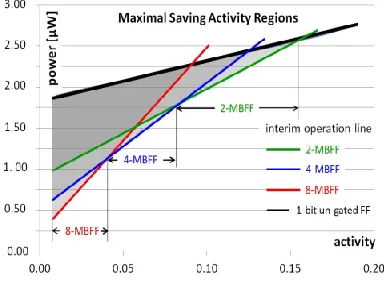
Fig. 3(a)–(c) illustrates that the power savings of the 2-MBFF, 4-MBFF, and 8-MBFF, respectively, are used. Knowing the activity p of an FF, the decision as to which MBFF size k it best fits follows the interim lines, lines (d). To obtain the per-bit power consumption, lines (d) in Fig. 3(a)–(c), representing an MBFF realistic operation, were divided by their respective multiplicity. The result is shown in Fig. 4.
Fig. 4: Division of the activity into ranges of maximal savings.
To maximize the power savings, Fig. 4 divides the range of FF activity into regions. The black line follows the power consumed by a 1-bit ungated FF. The triangular areas bounded by the black line and each of the green, blue, and red per-bit lines show the amountof power savings per activity obtained by grouping an FF in the 2-MBFF, 4-MBFF, and 8-MBFF, respectively. It shows that for a very low activity, it pays to group FFs into an 8-MBFF. As activity increases, there will be some point where the 4-MBFF overtakes and pays off more than the 8-MBFF. At some higher activity, the 2-MBFF overtakes and pays off more than the 4-MBFF, up to an activity where the power savings stops. The remaining FFs can be grouped into ungated MBFFs, simply to reduce the number of internal clock drivers. We take advantage of this behavior and the optimal grouping by the monotonic activity ordering shown in Section III.
The following MBFF grouping algorithm is proposed.
1) Sort the n FFs such that p1 ≤ p2 ≤ ··· ≤ pn.
2) i ← 1.
3) Decide on optimal k by pi , based on Fig. 4. 4) If i > n or k < 2 stop.
5) Group FFi, FFi+1. . . FFi+k−1 in a k-MBFF.
Few practical comments are in order. In addition to toggling probabilities, MBFF grouping should also consider logical relations and physical place and route constraints. An example is the pipeline registers of a microprocessor, which are natural candidates for MBFF implementation. It makes no sense to mix bits of different pipeline stages. It is obvious and natural that the place and route tool will put bits belonging to same register close to each other, while FFs clusters of registers belonging to distinct pipeline stages will be placed apart of each other. FFs of different pipeline registers should therefore be not mixed in a MBFF, although from toggling probability standpoint their grouping may be preferred. Similar arguments hold for other system’s busses and registers such as those storing data, addresses, counters, and alike. Another example is the FFs of Finite State Machines (FSMs) in control units, whose MBFF grouping should not cross control logic borders. Though the proposed algorithm is aimed at RTL or gate design levels, it can also be combined with the grouping methods proposed by [3-7]. There, an initial placement takes place as a “dry run” to obtain initial FFs’ layout proximity directives. The toggling probability-driven algorithm can then consider those to guide the MBFFs grouping. The later real place and route will use MBFF library cells, unlike [3-7] which rip up the old FFs and insert MBFFs replacements, a non-trivial and tedious layout task, which is saved by our design flow.
Finally, the aforementioned postplacement MBFF clustering must consider the timing constraints, which are built into their algorithms. By contrast, the MBFF grouping algorithm does not require explicit timing constraints since it works at the RTL design level. In order to bridge the gap between the RTL grouping and the grouping driven by backend timing-closure considerations, we suggested appropriate DDCG design flow. The main idea involves providing “natural” physical layout directives for FF grouping by employing a prior placement. The main steps are described below. More details can be found in [18]:
1) Estimation of the FFs toggling probabilities;
2) Running the placement to get preliminary preferred locations of FFs in the layout (dry run);
3) Using the proximity data of FFs’ physical locations to constraint probability-driven grouping;
4) Adding the DDCG logic to the Verilog HDL code (done automatically by the software tool);
5) Ordinary backend flow execution.
V. EXPERIMENTAL RESULTS
The proposed DDCG MBFF design flow was used for two designs: a 32-bit pipelined MIPS processor, implemented in a TSMC 65-nm technology, and an industrial network processor, implemented in a TSMC 28-nm technology. For the MIPS, a workload of sort and matrix multiplication programs was tested, as shown in Table I. The data-to-clock toggling probability for each FF was derived by simulating the workload on the RTL design. For each test, the average data-to-clock switching activity of an FF in the pipelined register is shown under the stage name. Observe the decrease in activity with the progress of the pipeline stage from instruction fetch to write-back.
The MBFF bits of the pipeline registers were grouped by monotonic activity. Table I shows the power savings obtained for the combined benchmark. Each pipeline stage shows the savings for implementation with an ungated MBFF and for DDCG integrated into MBFFs, as proposed here. The results were measured with SpyGlass [15] simulations where the MIPS processor was operated at 1.1 V and 200 MHz. whereas the ungated MBFF saved 18% of the total power, the integration of DDCG with MBFF yielded almost a double saving of 34.6%. The pipelined registers consumed 65% of the entire MIPS power (memory and IO excluded), so the total power reduction in the entire core was 23%, including the gating overheads.
the FF layout proximity. The results are shown in the postlayout rows of Table I. The front-end RTL grouping outperformed the postlayout, yielding nearly 41% more savings. The second experiment was a complete industrial network processor designed in the TSMC 28-nm technology. The processor operates in 800 MHz. It is divided into seven units, labeled A–G in Table II.
The original design already included extensive clock enabling logic signals and ungated MBFFs, inserted both by the RTL compiler and manually. Each unit contains many clock domains derived by logic conditions. The DDCG MBFF design flow worked on each clock domain separately. The network processor consumed a total of 6.2 W, of which 45% was charged to the clock network, including its underlying FFs. The original design comprised ungated MBFFs, so Table II shows the net power savings obtained solely by the DDCG addition shown in Fig. 2
TABLE I
POWER SAVINGS IN THE PIPELINE REGISTER OF A 32-BIT 65-nm MIPS
TABLE II
POWER SAVINGS OF A 28-nm NETWORK PROCESSOR
Table II shows an additional 8% net power saving on top of the ungated MBFFs in reference. The power measurements included both dynamic and static components and all the gating overheads. The 8% power savings comes on top of the 9% savings achieved using MBFFs in the original design, thus yielding 17% combined savings. Similar to the MIPS, this is about double the power savings compared with ungated MBFFs alone. Such savings are highly appreciated by the industry. The area penalty due to the introduction of CG circuitry was 2.3%.
VI.RESULTS
The composed Verilog HDL Modules have effectively recreated and confirmed utilizing Isim Simulator and orchestrated utilizing Xilinxise13.2.
Simulation results:
Technology Schematic:
Design summary:
Timing Report:
VII. CONCLUSION
This brief suggests combining MBFFs and probability-driven CG to increase their power savings. A model utilizing the relationship between the optimal MBFF multiplicities to FF data-to-clock toggling probabilities is used in a practical design flow, achieving 17% and 23% power savings, compared with designs with ordinary FFs. About half of these savings can be attributed to the integration of DDCG into MBFFs.
REFERENCES
[1] A. Kapoor et al., “Digital systems power management for high performance mixed signal platforms,” IEEE Trans. Circuits Syst. I, Reg. Papers, vol. 61, no. 4, pp. 961–975, Apr. 2014.
[2] S. Wimer and I. Koren, “The optimal fan-out of clock network for power minimization by adaptive gating,” IEEE Trans. VLSI Syst., vol. 20, no. 10, pp. 1772–1780, Oct. 2012.
[3] C. Santos, R. Reis, G. Godoi, M. Barros, and F. Duarte, “Multi-bit flipflop usage impact on physical synthesis,” in Proc. 25th IEEE Symp. Integr. Circuits Syst. Design (SBCCI), Sep. 2012, pp. 1–6.
[4] J.-T. Yan and Z.-W. Chen, “Construction of constrained multi-bit flipflops for clock power reduction,” in Proc. IEEE Int. Conf. Green Circuits Syst. (ICGCS), 2010, pp. 675–678.
[5] IH-R. Jiang, C-L. Chang, and Y-M. Yang, “INTEGRA: Fast multibit flip-flop clustering for clock power saving,” IEEE Trans. CAD Integr. Circuits Syst., vol. 31, no. 2, pp. 192–204, Feb. 2012.
[6] C. L. Chang and I. H. R. Jiang, “Pulsed-latch replacement using concurrent time borrowing and clock gating,” IEEE Trans. Comput.- Aided Design Integr., vol. 32, no. 2, pp. 242–246, Feb. 2013.
[8] T. Shyu, J.-M. Lin, C.-P. Huang, C.-W. Lin, Y.-Z. Lin, and S.-J. Chang, “Effective and efficient approach for power reduction by using multi-bit flip-flops,” IEEE Trans. VLSI Syst., vol. 21, no. 4, pp. 624–635, Apr. 2013.
[9] S. Liu, W.-T. Lo, C.-J. Lee, and H.-M. Chen, “Agglomerative-based flip-flop merging and relocation for signal wirelength and clock tree optimization,” ACM Trans. Design Autom. Electron. Syst., vol. 18, no. 3, article no. 40, Jul. 2013.
[10] M. P. H. Lin, C. C. Hsu, and Y. C. Chen, “Clock-tree aware multibit flip-flop generation during placement for power optimization,” IEEE Trans. Comput.-Aided Design Integr., vol. 34, no. 2, pp. 280– 292, Feb. 2015.
[11] C. Xu, P. Li, G. Luo, Y. Shi, and IH-R. Jiang, “Analytical clustering score with application to post-placement multi-bit flipflop merging,” in Proc. ACM Int. Symp. Phys. Design, 2015, pp. 93–100.
[12] S.-H. Wang, Y.-Y. Liang, T.-Y. Kuo, and W.-K. Mak, “Power-driven flipflop merging and relocation,” IEEE Trans. CAD Integr. Circuits Syst., vol. 31, no. 2, pp. 180–191, Feb. 2012.
[13] S-C. Lo, C-C. Hsu, and MP-H. Lin, “Power optimization for clock network with clock gate cloning and flip-flop merging,” in Proc. ACM Int. Symp. Phys. Design, 2014, pp. 77–84.
[14] S. Wimer, D. Gluzer, and U. Wimer, “Using well-solvable minimum cost exact covering for VLSI clock energy minimization,” Operations Res. Lett., vol. 42, no. 5, pp. 332–336, Jul. 2014.
[15] SpyGlass Power, accessed on 2016. [Online]. Available: http://www.atrenta.com/solutions/spyglass-family/spyglass-power.htm
[16] Y.-T. Chang, C.-C. Hsu, M. P.-H. Lin, Y.-W. Tsai, and S.-F. Chen, “Postplacement power optimization with multi-bit flip-flops,” in Proc. IEEE Int. Conf. (CAD), Nov. 2010, pp. 218–223.