High performance and high efficiency DET flip flop by using
Clock gating techniques
Thirupataiah Perla & Bandhu Mounika
#1Asst. Professor (Dept ECE), Sagar Institute of Technology Hyderabad-India #2M.TECH,(VLSI&ES), Sagar Institute of Technology Hyderabad-India
Abstract:
Dual edge triggered (DET) flip-flops achieve the same data rate as single edge triggered (SET) flip-flops at half the clock frequency, which can lead to reduced power dissipation of synchronous logic circuits. The cost of this reduction is higher circuit complexity of DET flip-flops which usually have more transistors and more internal nodes than SET flip-flops. In this paper, a novel Clock gating flip-flop (FF) design for high speed applications is presented. . Both total transistor count and the number of clocked transistors are significantly reduced to improve power consumption and speed in the flip-flop.
.
Introduction:
Today’s technologies make possible powerful computing devices with multi-media capabilities. Consumer’s attitudes are gearing towards better accessibility and mobility. Their desire has caused a demand for an ever-increasing number of portable applications requiring low-power and high throughput. For example, notebook and handheld computers are now made with competitive computational capabilities as those found in desktop machines. Equally demanding are personal communication applications in a pocket-sized device. In these applications, not only voice, but data as well as video are transmitted via wireless links. It is important that these high computational capabilities are placed in a low-power, portable environment. The weight and size of these portable devices is determined by the amount of
content transmitted over a given set of lines is increased, memory requirement for a given length of data is lowered, interconnections required to implement logic functions are reduced thereby reduction in chip area thus making VLSI implementations energy efficient and cost effective at the same time. Also, certain serial and serial-parallel operations are carried out at faster speeds. Numerous applications like digital signal processing, fuzzy logic, artificial intelligence, memories, communications, robotics, digital control systems and many more, have confirmed its applications. The design of multipliers in today’s advanced technology takes up any one or combination of the following design targets such as high speed, regularity of layout and hence less area in one multiplier, low power consumption thus making them adequate for a number of high speed, lower power and compact VLSI implementations. Three valued logic (3VL) based multiplier design offers the added advantage of circuit complexity being reduced in terms of both device count and inter connections. It is a very slow operation which also depends on the word size to be executed where large number of partial products (PPs) needs to be computed to produce the final result. So they should be fast enough to give the output in the required cycle time. Recently, because of the rapid growth of battery-powered, high-performance and portable electronic devices, the power consumption of VLSI chip has gained extraordinary consideration. It is known that the power consumption determines the device’s battery life as well as the time between two successive recharges of a device so what assumes importance is the reduction of power dissipation in such devices. Various techniques for reducing the power consumption are applied externally or internally in digital multipliers. Techniques which deal with the input data characteristics are external techniques, whereas those concerned with the logic, architecture and circuit designs of the multiplier are internal ones.
C-ELEMENT:
A C-element, introduced in, is normally a three-terminal device with two inputs and one output. When all of its inputs are the same, the output switches to the value of the inputs. When the inputs are not the same, the previous output value is preserved. This device acts as a latch which can be set and reset with appropriate combinations of signal levels at the input.
FIG: 1(a) non inverting (b) inverting using C-ELEMENTS.
DUAL EDGE TRIGGERED FLIP-FLOP:
In a synchronous system, operations and data sequences take place with a fixed and predetermined time relationship. The timing of computations is controlled by flip-flops and latches together with a global clock. Flip-flops and latches are clocked storage elements, which store values applied to their inputs. They are classed according to their behavior during the clock phases. A latch is level sensitive. It is transparent and propagates its input to the output during one clock phase (clock low or high), while holding its value during the other clock phase. A flip-flop is edge triggered. It captures its input and propagates it to the output at a clock edge (rising or falling), while keeps the output constant at any other time. The design of this clocked storage an element is highly depended on the clocking strategy and circuit topology .This research focuses on synchronous system with edge-triggered clocking strategy, henceforth, only flip-flop is discussed. In particular, dual edge-triggered flip-flops are introduced and explored.
Fig.2 floating-node FN_C
In the IP_C flip-flop, signal levels at A and B toggle after every clock transition regardless of D and Q, which leads to higher power dissipation due to clock signal transitions. The transistor-level and gate-level schematic diagrams of the improved FN_C flip-flop that solves this issue. In the case of the LG_C, IP_C, and FN_C flip-flops, for the output C-element to work correctly, the requirements for the flip-flop’s input stage are as follows: In between the clock edges, at least one of A and B has to be kept at Q to avoid flipping at the output, and once the clock toggles, both nodes have to be at D for the output to switch to D. As long as one of A and B is kept at Q, the signal level at the other node is irrelevant for the correct operation of the output stage. With implementations of C-elements, one of A and B that is not kept at Q can be at any permitted voltage level without affecting the output. The LG_C flip-flop satisfies these requirements by employing two independent latches at A and B, one of which is always redundant (which one depends on D and CK). The implicit-pulsed IP_C flip-flop ensures
node B switches to ―0.‖ Both A and B are now at ―0,‖ which causes the output C-element to switch Q to ―1.‖ Node A is floating again and B is kept at ―0,‖ which ensures that Q stays at ―1‖ in the new cycle. In this example, the combinations of D and CK are such that only node A is seen floating. If either D or CK were inverted, node B would have been the floating node. Because of the switching of parasitic capacitances before floating node events, floating voltage levels at A and B can stay above the VDD voltage of 0.85 V or below 0 V. Analog simulations indicate that the increase above VDD and the decrease. Transistor-level schematic diagram of the conditional-toggle CT_CDET flip-flop. Simulated signal levels of the CT_C flip-flop implemented in the 28nm GF 28HPP technology. below 0 V do not exceed 10% of the nominal VDD and that no significant dynamic current is flowing through the transistors’ channels during this time. Thus, floating node events do not affect circuit reliability.
D. Conditional-Toggle CT_C and CTF_C Flip-Flops:
Fig 3.Schematic diagram of the conditional-toggle CT_CDET flip-flop.
The novel conditional-toggle CT_C DET flip-flop design. The CT_C flip-flip-flop circuit uses only20 transistors including transistors for the input, output, and clock buffering. The flip-flop consists of a dynamic C-element at the output
more energy It takes to change the state of the latch, i.e., the higher the power dissipation at low switching activity becomes. Fig. 15 shows the CTF_C flip-flop, a modification of the CT_C flip-flop, that relaxes these trade-offs.
During operation one of A or B nodes is at D while the other is at D. In the CTF_C flip-flop, the strengths of signal levels at these nodes depend not only on transistor sizing but also on D:Which ever node is at D is kept strongly while the other node is kept weakly with always-on transistors. If at a clock transition D is not equal to Q, node X is multiplexed to a strong D that quickly changes X to D and Q to D. When D is equal to Q, logic level at node X is kept strongly at D by the C-element. The next clock transition multiplexes node X to a weak D which the C-element overpowers quickly and at a low energy cost. Thus, CTF_C achieves faster switching compared to CT_C and reduces energy dissipation of idle cycles.
Fig.4 Schematic diagram of the improved conditional-toggle CTF_C DET flip-flop.
A. Clock Gating Technique:
Several techniques to reduce the dynamic power have been developed, of which clock gating is predominant. Ordinarily, when a logic unit is clocked, its underlying sequential elements receive the clock signal regardless of whether or not they will toggle in the next cycle. Clock enabling signals are usually introduced by designers during the system and clock design phases, where the inter-dependencies of the various functions are well understood. In
contrast, it is very difficult to define such signals in the gate level, especially in control logic, since the inter-dependencies among the states of various flip-flops depend on automatically synthesized logic. There is a big gap between block disabling that is driven from the HDL definitions, and what can be achieved with data knowledge regarding the flip-flops activities and how they are correlated with each other. The clock gating technique has been developed to avoid unnecessary power consumptions, like the power wasted by timing components during the time when the system is idle. Specifically for flip-flops, clock gating means disabling the clock signal when the input data does not alter the stored data. It can be applied from the system level where the entire functional unit can be selectively set into sleep mode, or from the sequential/combinational circuit level where some parts of the circuit are in sleep mode while the rest of the block are operating. But Clock gating does not come for free. Extra logic and interconnects are required to generate the clock enabling signals, and the resulting area and power overhead must be considered [5]. In the extreme case, each clock input of a flip-flop can be disabled individually, yielding maximum clock separation. This, however, results in high overhead. Thus, the clock disabling circuit is shared by a group of several flip-flops in an attempt to reduce the overhead.
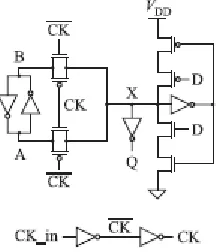
B. How to implement Clock Gating?
Fig: 5 Clock gating circuit
Result analysis:
Fig:6 LG_DET FF
Fig:7 IP_DET FF
Fig:8 FN_DET FF
Fig9 :CTC_DET FF
Fig:10 Clock gating technique based DET flipflop
Fig:11 Waveform for flipflop
Tabulation:
Type Power
consumption
Delay
LG_DET
4.547539e-003 watts 1.0000e-007
Implicit
pulsed 2.399687e-004 watts 5.2500e-008
FN DET
2.473412e-004 watts 5.2500e-008
CTC_DET
6.207332e-005 watts
Clock gating technique
2.449398e-006 watts 5.2500e-008
Conclusion:
In this paper, a novel low-power pulse triggered flip-flop (ff) design is presented. If optimization is applied it is possible to achieve much higher speeds .it is then concluded that the proposed novel implicit pulsed-data close to output appears to be the most suitable storage element in high-speed, low-power VLSI applications. The pulse trigged, consume less power and delay compare with existing.
References:
[1] N. Nedovic and V. G. Oklobdzija, ―Dual-edge triggered storage elementsand clocking strategy for low-power systems,‖ IEEE Trans. Very LargeScale Integr. (VLSI) Syst., vol. 13, no. 5, pp. 577–590, May 2005.
[2] A. G.M. Strollo, E. Napoli, and C. Cimino, ―Analysis of power dissipationin double edge-triggered flip-flops,‖ IEEE Trans. Very Large Scale Integr.(VLSI) Syst., vol. 8, no. 5, pp. 624– 629, Oct. 2000.
[3] P. Zhao, J. McNeely, P. Golconda, M. A. Bayoumi, R. A. Barcenas, andW. Kuang, ―Low-power clock branch sharing double-edge triggered flipflop,‖IEEE Trans. Very Large
Scale Integr. (VLSI) Syst., vol. 15, no. 3,pp. 338– 345, Mar. 2007.
[4] J. Tschanz, S. Narendra, C. Zhanping, S. Borkar, M. Sachdev, and V. De,―Comparative delay and energy of single edge-triggered and dual edgetriggeredpulsed flip-flops for high-performance microprocessors,‖ Proc.Int. Symp.Low Power Electron.Des., 2001, pp. 147152.
[5] D. E. Muller, ―Theory of asynchronous circuits,‖ Internal Rep. no. 66,Digit. Comput.Lab., Univ. Illinois at Urbana-Champaign, 1955.
[6] K. van Berkel, ―Beware the isochronic fork,‖ Integr., VLSI J., vol. 13,pp. 103–128, Jun. 1992. [7] S. V. Devarapalli, P. Zarkesh-Ha, and S. C. Suddarth, ―A robust and lowpower dual data rate (DDR) flip-flop using C-elements,‖ in Proc. 11th Int.Symp. Quality Electron.Des. (ISQED), Mar. 22–24 2010, pp. 147–150.
[8] A. Gago, R. Escano, and J. A. Hidalgo, ―Reduced implementation ofD-type DET flip-flops,‖ IEEE J. Solid-State Circuits, vol. 28, no. 3,pp. 400–402, Mar. 1993.
[10] A. Bonetti, A. Teman, and A. Burg, ―An overlap-contention free truesingle-phase clock dual-edge-triggered flip-flop,‖ in Proc. IEEE Int.Symp. Circuits Syst. (ISCAS), May 24–27 2015, pp. 1850–1853.
[11] M. Alioto, E. Consoli, and G. Palumbo, ―Analysis and comparisonin the energy-delay-area domain of nanometer CMOS flip-flops: PartI—Methodology and design strategies,‖ IEEE Trans. Very Large ScaleIntegr. (VLSI) Syst., vol. 19, no. 5, pp. 725–736, May 2011. [12] M. Alioto, E. Consoli, and G. Palumbo, ―Analysis and comparisonin the energy-delay-area domain of nanometer CMOS flip-flops: PartII—Results and figures of merit,‖ IEEE Trans. Very Large Scale Integr.(VLSI) Syst., vol. 19, no. 5, pp. 737–750, May 2011.
[13] V. Stojanovic and V. G. Oklobdzija, ―Comparative analysis of masterslavelatches and flip-flops for high-performance and low-power systems,‖IEEE J. Solid-State Circuits, vol. 34, no. 4, pp. 536–548, Apr. 1999.
[14] M. Alioto, E. Consoli, and G. Palumbo, ―Analysis and comparison ofvariations in double edge triggered flip-flops,‖ in Proc. 5th Eur. WorkshopCMOS Variability (VARI), Palma de Mallorca, Spain, 2014, pp. 1–6.
[15] M. Shams, J. C. Ebergen, and M. I. Elmasry, ―Modeling and comparingCMOS implementations of the C-element,‖ IEEE Trans.