Low-Power And Area-Efficient Shift Register Utilizing Beat Latches
P.Mahesh Babu & A.Rama Satya Balaji
1M-Tech, Dept. of ECE in Mallareddy Engineering College
2Asst. prof, Dept. of ECE in Mallareddy Engineering College
ABSTRACT
This paper proposes a low-power and zone
effective move enlist using beat locks. The
range and power utilization are lessened by
superseding flip-flops with beat locks. This
technique settles the planning bind between
beat hooks through the use of different
non-cover postponed beat check motions instead
of the regular single beat clock flag. The
move enroll uses a modest number of the
beat clock motions by gathering the locks to
a few sub shifter enlists and using incidental
fleeting stockpiling hooks. A 256-piece move
enlists using beat hooks was outlined using
Verilog HDL. The proposed move enroll jam
region and power contrasted with the
customary move enlists with flip-flops.
Key words: - Area-Efficient, Flip-Flop, Pulsed Clock, Pulsed Latch, Shift Register.
INTRODUCTION
Low power utilization and zone
diminishment are one of the primary
destinations in the planning of VLSI outline.
[1]The Shift enlist is the simple building
obstruct in VLSI circuits. It is regularly used
in numerous applications. The design of
move enroll is very basic. The M bit move
enlist can be is made out of M information
flip-flops. The most little flip-flops are
fitting for the planning of move enlist to
lessen the region and power utilization. The
Flip-flops is an information stockpiling
component. The operation of the flip-flops is
finished by its clock recurrence. Whenever
multistage Flip-Flop is worked with a
concession to clock recurrence, it forms with
high clock exchanging movement and after
that builds time idleness. Therefore it
influences the celerity and vitality execution
of the circuit. Sundry classes of flip-flops
have been proposed to accomplish the fast
and low-vitality operation. In the previous
decades, many works have been committed
to enhancing the execution of the flip-flops.
Locks and flip-flops are the basic
components for putting away data. The
flip-flounders and locks could be assembled
under the static and dynamic outline styles.
[7]One hook or flip-flounder can store one
between locks and flip-flops is that for
latches, their yields are unendingly
influenced by their contributions as long as
the empower flag is stated.When they are
empowered, their content changes instantly
when their data sources change. Flipflops,
then again, have their substance change just
either at the raising or falling edge of the
empower flag. This empower flag is usually
the controlling clock flag. After the lifting
or, on the other hand falling edge of the
clock, the flip-slump content remains steady
regardless of the possibility that the info
changes. Philosophy has been produced
which utilizes locks activated with heartbeat
the clock waveforms. With this philosophy,
timing investigation and timing
improvement to a lock plan while lessening
the puissance of the clock systems can get.
A lock can catch information amid the
delicate time dictated by the width of clock
waveform. In the event that the beat clock
waveform triggers a hook, [6]the lock is
synchronized with the clock correspondingly
to edge-activated flip-flounder on the
grounds that the raising and falling edges of
the beat check are essentially
indistinguishable as far as timing. With this
approach, the portrayal of the setup times of
beat lock are communicated with veneration
to the raising edge of the beat clock, and
hold times are communicated with reverence
to the falling edge of the beat clock. This
assigns the portrayal of timing models of
beat locks is related to that of the edge
triggered flip-slump. On the off chance that
the beat lock has been superseded with
flip-tumbles in the outlining of move enlist the
region and power utilization can be lessened
to half .Thus the move enlist can fathom
timing situation by the use of various
non-cover postponed beat check motions in lieu
of the traditional single beat clock flag.
These hooks and flip flounder outlines are
made by using 90nm innovation in DSCH2
schematic execute furthermore,
MICROWIND configuration execute.
2. RELEGATED WORK 2.1Existing System
A move enroll is the simple building
obstruct in a VLSI circuit. Move registers
are regularly utilized in numerous
applications, for example, computerized
channels [9], correspondence beneficiaries
[10], and picture handling ICs [1] - [3]. As
of late, by the size of the picture information
sustains to increase due to the appeal for
amazing picture information, the word
length of the shifter enlist increments to
information in picture preparing ICs. A
picture extraction and vector era VLSI chip
use a 4K-bit move enlist [8]. A 10-bit 208
channel yield LCD section driver IC uses a
2K-bit move enlist [2]. A 16-megapixel
CMOS picture sensor uses a 45K-piece
move enroll [4].
2.2Proposed System
In the proposed framework to transmute the
SSASPL furthermore, lessen the power level
of the move registers. [5]All beat hooks
share the beat era circuit for the beat clock
flag. Therefore, the territory and power
utilization of the beat hook turns out to be
for all intents and purposes an moiety of
those of the ace slave flip-slump. The beat
lock is a charming arrangement for the little
territory and low power utilization. The beat
lock can't be used in move registers because
of the planning pickle 3. IMPLEMENTATION 3.1Translate:
This procedure amalgamates all the
information netlists and requirements to a
rationale configuration record. This data is
safeguarded as an NGD (Native Generic
Database) record. This should be possible
using NGD Build program. Here,
characterizing requirements is only,
appointing the ports in the outline to the
physical components (ex. pins, switches,
catches and so on) of the focused on creation
and assigning time imperatives of the
outline. This data is put away in a document
designated UCF (Utilizer Constraints File).
Executes used to cause or adjust the UCF
are PACE, Constraint Editor and so on.
3.2 Guide:
This procedure isolates the entire circuit
with coherent components into sub pieces to
such an extent that they can be fit into the
FPGA rationale squares. That connotes
outline fits the rationale characterized by the
NGD document into the focused on FPGA
components (Combinational Logic Blocks
(CLB), Input Output Blocks (IOB)) and
caused an NCD (Native Circuit Description)
record which physically speaks to the plan
mapped to the segments of FPGA. Guide
program is used for this indicate.
3.3 PLACE AND ROUTE:
Standard program is used for this procedure.
The place and course process puts the sub
obstructs from the guide procedure into
rationale hinders as indicated by the
limitations and interfaces the rationale
squares. Ex. on the off chance that a sub
piece is set in a rationale square which is
extremely proximate to IO stick, at that
might impact some other requirement. So
exchange off between every one of the
requirements is considered by the place and
course process. The PAR actualize takes the
mapped NCD record as info and induces a
perfectly steered NCD document as yield.
Yield NCD document comprises the steering
data.
4. EXPERIMENTAL RESULTS
Fig 1 Block Diagram Of Pulsed Latches
Fig 2 Rtl Of Pulsed Latches
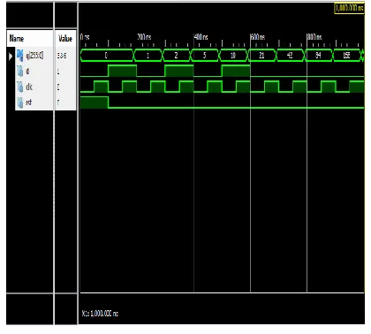
Fig 3 Simulation Results For Pulsed Latches
5. CONCLUSION
This venture proposed a low-power and
territory productive move enroll using beat
locks. The move enlists decreases region
and power utilization by superseding
flip-flops with beat hooks. The planning
dilemma between beat locks is unraveled
using different non-cover postponed beat
check motions insteadss of a solitary beat
clock flag. A modest number of the beat
clock signals is used by gathering the hooks
to a few sub shifter enlists and using
supplemental fleeting stockpiling locks. A
256-piece move enlist was manufactured.
The proposed move enroll jam 37% territory
and 44% power contrasted with the
6. REFERENCE
[1] IEEE TRANSACTIONS ON CIRCUITS AND SYSTEMS—I: REGULAR PAPERS, VOL. 62, NO. 6, JUNE 2015 Byung-Do Yang Low-Power and Area-Efficient Shift Register Using
Pulsed Latches.
[2] M. Hatamian et al., “Design considerations for gigabit ethernet 1000 base-T twisted pair transceivers,” Proc. IEEE Custom Integr. Circuits Conf., pp. 335–342, 1998.
[3] H. Yamasaki and T. Shibata, “A real-time image-feature-extraction and vector-generation vlsi employing arrayed-shift-register architecture,” IEEE J. Solid-State Circuits, vol. 42, no. 9, pp. 2046–2053, Sep. 2007.
[4] H.-S. Kim, J.-H. Yang, S.-H. Park, S.-T. Ryu, and G.-H. Cho, “A 10-bit column-driver IC with parasitic-insensitive iterative charge-sharing based capacitor-string interpolation for mobile active-matrix LCDs,” IEEE J.Solid-State Circuits, vol. 49, no. 3, pp.766–782, Mar.2014.
[5] S.-H. W. Chiang and S. Kleinfelder, “Scaling and design of a 16-megapixel CMOS image sensor for electron microscopy,” in Proc. IEEE Nucl. Sci. Symp. Conf. Record (NSS/MIC), 2009, pp. 1249–1256.
[6] S. Heo, R. Krashinsky, and K. Asanovic, “Activity-sensitive flip-flop and latch selection for reduced energy,” IEEE Trans. Very Large Scale Integr. (VLSI) Syst., vol. 15, no. 9, pp. 1060–1064, Sep. 2007.
[7] S. Naffziger and G. Hammond, “The implementation of the nextgeneration 64 b itanium microprocessor,” in IEEE Int. Solid-State Circuits Conf. (ISSCC) Dig. Tech. Papers, Feb. 2002, pp. 276–504.
[8] H. Partovi et al., “Flow-through latch and edge-triggered flip-flop hybrid elements,” IEEE Int. Solid-State Circuits
Conf. (ISSCC) Dig. Tech. Papers, pp. 138– 139, Feb. 1996.
[9] E. Consoli, M. Alioto, G. Palumbo, and J. Rabaey, “Conditional push-pull pulsed latch with 726 fJops energy delay product in 65 nm CMOS,” in IEEE Int. Solid-State Circuits Conf. (ISSCC) Dig. Tech. Papers, Feb. 2012, pp. 482–483.
[10] V. Stojanovic and V. Oklobdzija, “Comparative analysis of masterslave latches and flip flops for high-performance and low-power systems,” IEEE J. Solid-State Circuits, vol. 34,no. 4, pp. 536–548, Apr. 1999.
Author Profile P.MAHESH BABU
This is P.MAHESH BABU. I am pursuing
M-Tech in MALLAREDDY ENGINEERING
COLLEGE in specialization of VLSI SYSTEM
DESIGN and I got “O” grade in the first year of
M-Tech. and I completed my B-Tech in the
branch of ECE in the year 2015. I got “73.48 %”
in the B-Tech in SAI SPURTHI INSTITUTE