SMALL SIZE KA-BAND DISTRIBUTED MEMS PHASE SHIFTERS USING INDUCTORS
S. Afrang and B. Y. Majlis
Institute of Microengineering and Nanoelectronics (IMEN) University Kebangsaan Malaysia
43600 Bangi,Selangor,Malaysia
Abstract—MEMS phase shifter has been developed using inductors. The design consists of a CPW line capacitively and inductively loaded by the periodic set of inductors and electrostatic force actuated MEMS switches as capacitors. By applying a single bias voltage on the line, the characteristic impedance can be changed,which in turn changes the phase velocity of the line and creates a true time delay phase shift. The governing equations for the impedance and loss are derived. The ABCD matrix is defined for a unit cell and multi-cell DMTL phase shifter to extract scattering parameters equations. The MEMS switch is actuated by a 39 voltage waveform using a high resistance bias line. Estimated spring constant and switching time is 22 N/m and 3µs,respectively. The structure is designed for Ka-band frequency range. The acceptable frequency range for the design containing 21 cells is between 26 GHz and 27 GHz and optimum condition occurs at 26.3 GHz. For the whole structure and optimum condition the un actuated position results in a return loss−16 dB and insertion loss of
−1.65 dB. The actuated position results in a return loss −12.5 dB and insertion loss of−1.6 dB. The phase shift for the whole structure is 190 degree. The optimum condition can be easily changed by modifying
the design parameters. The spacing in the proposed structures is
S = 250µm. The structure is also low loss. The length and the loss per bit with the phase shift of 270◦ are decreased by 37.5 percent and 21 percent respectively.
1. INTRODUCTION
demonstrated broad-band characteristics with low loss [3]. However, since there was a limit on the control range of the bridge height before the bridge snaps,the analog phase shifter showed relatively small phase shift. This problem was solved by operating the MEMS bridges in the digital mode [4–11],where two distinct capacitance states (ON and OFF) were defined with a high ratio. Digital phase shifters with this approach allow large phase shift and low sensitivity to electrical noise. In the published CPW digital phase shifters [4,5], a small metal-insulator-metal (MIM) capacitor or metal-air-metal (MAM) [10,11] in series with the MEMS bridge capacitor was used to reduce the total shunt capacitance seen by the line,resulting in an acceptable return loss for both switching states over a wide band.
This work presents a new concept of distributed MEMS true time delay phase shifters using both inductors and capacitors. As it is known,the inductor changes the phase of a signal same as the capacitor. In our distributed MEMS transmission line (DMTL) design, MEMS switches and inductors are used to change loading capacitance and inductance on a high-impedance t-line such that the return loss is within an acceptable range for the two phase states (with the MEMS switches in the up- and down-state positions). Traditionally, commercially available phase shifters are based on ferrite materials,p-i-n diodes or FET switches but they consume power more than MEMS based phase shifters. There is a drawback using MEMS phase shifters. MEMS based phase shifters have large size. It is essential that the
area of a RF MEMS phase shifter be reduced. The advantages of
decreased area are much higher part count per wafer,easier hermetic packaging and much lower coast. The goal of the design in this paper is to decrease the size of the structure by maintaining the maximum amount of phase shift with the minimum amount of insertion loss and with a low return loss per unit cell.
2. MODELING AND DESIGN EQUATIONS
Coplanar wave-guide (CPW) transmission line has been used for the design. Figure 1 shows a unit cell MEMS phase shifter on a glass substrate.
There are two MEMS bridges,two capacitors and one inductor in the structure. One of the bridges is in the shunt configuration
and connects the inductor to the AC capacitor. Another bridge is
RF connector plate Shunt MEMS Bridge
inline MEMS Bridge
Bias Line
inductor
DC plate dielectric layer
RF connector plate Bias Line DC plate Centre conductor Ground Ground s ubstrate
RF connector plate Bias Line
DC plate
RF connector plate Bias Line DC plate Centre conductor Ground Ground s ubstrate
RF connector plate Shunt MEMS Bridge
inline MEMS Bridge
Bias Line
inductor
DC plate dielectric layer
RF connector plate Bias Line
DC plate
RF connector plate Shunt MEMS Bridge
inline MEMS Bridge
Bias Line
inductor
DC plate dielectric layer
RF connector plate Bias Line DC plate Centre conductor Ground Ground s ubstrate
RF connector plate Bias Line
DC plate
RF connector plate Bias Line
DC plate
RF connector plate Bias Line
DC plate
RF connector plate Bias Line DC plate Centre conductor Ground Ground s ubstrate
Figure 1. The schematic of proposed DMTL phase shifter (unit cell).
plate and another end is grounded. There are two capacitors under the inline MEMS bridge. The plate under the dielectric layer together with the inline MEMS bridge makes DC capacitor. The DC voltage is applied to this capacitor using a single high-resistance bias line. Another capacitor is AC capacitor. The plate on the dielectric layer (RF connector plate) together with the inline MEMS bridge makes AC capacitor in the up state (un-actuated) position. The AC capacitor only exists in the up-state position.
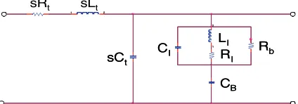
Figure 2 shows the equivalent circuit of the proposed structure in the up state position. In this circuit,the distributed parameters for the impedance of transmission line have been used where Lt, Ct and Rt are per unit length inductance,capacitance and resistance of the transmission line respectively,and “s” is the periodic separation.
RI, LIandCIare the series resistance,inductance and the capacitance of the coil respectively. The AC capacitance of inline MEMS bridge is
1 2 1 2 Rb LI RI CB
sCt CI
1 2 1 2 Rb LI RI CB sCt sLt sRt CI
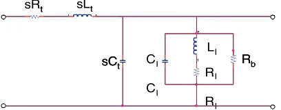
shown byCB. The bias line resistance Rb is in parallel with inductor. When the voltage is applied to the inline MEMS bridge,the bridge moves down and makes required contact with the RF connector plate. Therefore,the ungrounded end of the inductor is connected to the center conductor. In this condition,the inductor is connected in parallel to the center conductor. Figure 3 shows the equivalent circuit of the structure in the down state (actuated) position.
1 2
Rb
I
RI
sCt
sLt
sRt
CI
1 2
Rb
LI
R
sCt
t t
CI
1 2
1 2
Figure 3. The equivalent circuit in the down state position.
Figure 4 shows the distributed circuit model for the phase shifter. It consists of a unit cell which is cascaded multiple times in a t line circuit. Each unit cell is capable of certain amount of phase shift and by adding more cells the total phase shift increases by a factor of the number of cells.
ZS /2 ZS ZS ZS /2
unit cell
YP YP YP
ZS /2 ZS ZS ZS /2
YP YP YP
ZS /2 ZS ZS ZS /2
YP YP YP
ZS /2 ZS ZS ZS /2
YP YP YP
Figure 4. The general model for a distributed transmission line.
Considering Figure 4,the characteristic impedance for a distributed line is given by [12],
Zo =
Zs
Yp
1 +ZsYp
4 (1)
in the up state position the loadedt-line impedance is given by:
Zu=
−ω·sLtRq·CU+jsLt(1−ω2·LI·CU)
−ω(sCtRqCu+CICBRq)+j[sCt(1−ω2LICU)+CB(1−ω2CILI)]
1+−ω 2sL
t[sCt(1−ω2LICU)+CB(1−ω2CILI)+jωRq(sCtCU+CBCI)] 4 (1−ω2·L
I·CU +jωRq·CU)
(2)
Where,
Rq=RI+ (ωLI)2/Rb (3)
and,
CU =CI+CB (4)
As equation (2) shows,there are two resonance frequencies in the up state position and are given by:
fr1(up) =
1 2π√LI·CU
(5)
fr2(up) = 1 2π√LI·CI
(6)
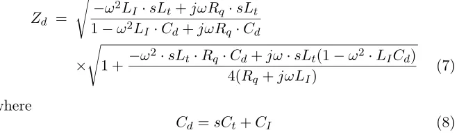
Using general model for the proposed structure and by considering Figure 3 the loaded t-line impedance in the down state position is given by:
Zd =
−ω2L
I·sLt+jωRq·sLt 1−ω2L
I·Cd+jωRq·Cd
×
1 +−ω 2·sL
t·Rq·Cd+jω·sLt(1−ω2·LICd) 4(Rq+jωLI)
(7)
where
Cd=sCt+CI (8)
As equation (7) shows,there is one resonance frequencies in the down state position and is given by:
fr(down)= 1 2π√LICd
(9)
The per unit length inductance and capacitance of a transmission line are determined to be [13],
Lt =
√ε
r,eff ·Zo
c (10)
Ct =
√ε
r,eff
Zo·c
(11)
Where, εr,eff is the effective dielectric constant of the unloaded line
and c/√εr,eff is the guided velocity of the high-impedance CPW line
without any loading.
The pull down voltage and the switching time are found to be [13],
Vp ∼=
8kg03
27εA. (12)
t = 3.67 Vp
Vsω0
, (13)
Where, k,and ω0 are the spring constant and resonance frequency of the MEMS bridge,respectively. Vs, g0 and A,are the applied voltage, gap distance and the area between the DC plate and MEMS bridge, respectively.
For a beam over a CPW line with the center conductor a third of the length of the beam,the spring constant is given by [13],
K = 32Ewt 3
l3
27 49
+8σ(1−v)wt
l
3 5
(14)
Where E, w, l, t, v,and σ are Young’s modulus,width,length,
thickness,Poisson’s ratio and biaxial residual stress of the MEMS bridge respectively.
The resonance frequency for the fixed-fixed beam bridge is given by [14],
ω2 = l
0
EI
d2y(x)
dx2 2
dx
l
0
ρA[y(x)]2dx
(15)
the deflection at any distancexalong the length of the bridge and are given by,
I = wt 3
12 (16)
y(x) = F x 2
48EI(4x−3l) (17)
3. DERIVATION OF SCATTERING PARAMETERS AND LOSS COMPONENTS
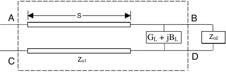
The distributed line phase shifter can be conveniently analyzed using
the ABCD matrices. To derive S11 in terms of ABCD-parameters,
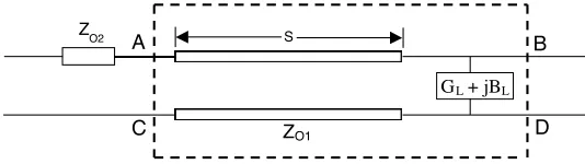
the equivalent circuit in Figure 5 has been used. In this circuit, ZO2 is a matched transmission line. ZO1 is the characteristic impedance of the lossy transmission line. The length of the lossy transmission line determines the periodic separation. The structure is placed over this line. The term (GL+jBL) is the shunt load.
S
GL + jBL
C
A B
D
Zo1
Zo2
Figure 5. Circuit for derivation ofS11.
S11 in terms of ABCD-parameters of the structure and matched transmission line ZO2 is as following [15]:
S11=
A+B·YO2−C·ZO2−D
A+B·YO2+C·ZO2+D
(18)
The ABCDmatrix of the lossy transmission line is given by:
A B C D =
cosh(γ·s) ZO1·sin(γ·s)
YO1·sinh(γ·s) cosh(γ·s) (19)
γ = α+jβ (20)
Where, γ, αand β are the complex propagation constant,attenuation and the phase constant of the transmission line respectively.
TheABCD matrix of the shunt load is given by:
A B C D =
1 0
By considering the serial combination of inductor and ac capacitance of MEMS bridge,GLandBLfor the structure in the up state position is given by:
GL(up)=−
ω2CBCIRI[1−ω2L(CB+CI)]+ω2CBRI(CI+CB)(1−ω2LCI) [1−ω2L(C
B+CI)]2+ω2R2I(CI+CB)2
(22)
BL(up)=ωCB(1−ω 2LC
I)(1−ω2L(CB+CI) +ω3CBCIR2I(CI+CB) [1−ω2L(C
B+CI)]2+ω2R2I(CI+CB)2
(23) For the design in the down state position the shunt load consists of only inductor. Therefore,GLandBLfor the structure in the actuated position are as following:
GL(down = RI
RI2+ω2L2 I
(24)
BL(down = ωR 2
ICI−ωLI(1−ω2LICI)
R2I+ω2L2 I
(25)
The overallABCD matrix of the structure is obtained as:
A B C D =
cosh(γ·s) ZO1·sinh(γ·s)
YO1·sinh(γ·s) cosh(γ·s) ·
1 0
GL+jBL 1 (26) To deriveS21in terms of ABCD-parameters,the equivalent circuit in Figure 6 has been used. The source impedance ZO2 must be included in the calculation to separate incident and reflected waves. S21in terms of ABCD-parameters is as following:
S21=
2
A+B·YO2+C·ZO2+D
(27)
The ABCD matrix of the structure has not been changed and is
obtained from equation (26). There are two contributors to the
B
S
ZO1
ZO2
C A
GL + jBL
D
insertion loss of the structure. They consist of conductor loss and Q
loss in the shunt loading inductor. The inductorQloss is the combined loss of inductor resistor and bias line resistor. The bias lines have a significant effect on the overall insertion loss performance of the phase shifter because they decrease the effectiveQof the structure.
The lossy static inductor is modeled as, RS,in series with LI (or a resistance RP,in parallel with LI). The inductor Qcan be written as:
Q= ω·LI
RS
= RP
ω·LI
(28)
(28) where,
RS =
(ω·LI)2
RP
(29)
Bias line resistance is in parallel with inductor. Therefore,considering the equation (29) the total resistance in the shunt section is equal to the series resistance, RI,due to theQ of the inductor,plus equivalent series bias line resistance,
Rq=RI+ (ωLI)2/Rb (30)
There are two methods to calculate the loss of the structure. One method is to extract the loss from S-parameters. The S21 does not necessarily indicate power loss in the unit cell,but can simply be due to the reflected power from the structure. The loss of the structure is better derived from the S-parameters as:
Loss = 10 log|S21|2−10 log(1− |S11|2) dB (31)
In another method consider a transmission line which is represented by a series inductance and resistance per unit length,Lt and Rt,and by a shunt capacitance and admittance per unit length, Ct and Gt, respectively,the attenuation constantα is given by [16]
α= Rt 2Z +
GtZ 2
N p
unilength (32)
In a planar transmission line such as CPW, Rt represents the
transmission line conductor loss,andGt represents the dielectric loss. The corresponding t-line lossα for the proposed structure is:
α∼= 8.686
Rt 2Zo
+GL·Zo 2
dB/section (33)
where, GL represents the shunt loaded loss in the up or down
placed within this system [15]. Most TEM transmission line systems have 50-ohm characteristic impedance so that when the characteristic impedance is not specified,50 ohm is assumed. The transmission-line loss equation related to physical parameters of the unloaded CPW line is found from a conformal mapping technique,and is given by Hoffmann [17]
αc=Ff
8.686Rs√εr,eff
4ηSK(k)K(k)(1−k2)
×
2S W
π+ln
4πW(1−k)
t(1+k) +2
π+ln
4πS(1−k)
t(1+k)
dB/m
(34)
whereFf is a fudge factor (Ff = 1.47 for 30 GHz) since equation (34) follows the correct trend for loss vs. impedance. It should be noted that this equation significantly underestimates the measured loss of the CPW line on Pyrex. The resistive per unit length is given by [18]:
R= ρ
δ·W (35)
Where,ρ (Ω-m) is the metal resistivity,wis the width of the line,and
δ is the skin depth given by:
δ=
ρ
π·µ·f (36)
Where, µis the permeability of free space. In practice,the resistivity of plated materials are around 1.3–1.5 times higher than bulk values presented by equation (35). For evaporated materials the resistivity is about 2 time,more than bulk values.
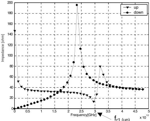
4. KA-BAND DMTL PHASE SHIFTER DESIGN
0 0.5 1 1.5 2 2.5 3 3.5 4 4.5 5 x 10¹⁰ 0
20 40 60 80 100 120 140 160 180 200
Frequency[GHz]
up down
fr1 (up)
Impedance [ohm]
Figure 7. Characteristic impedance diagrams in the up and down state position.
The first step in the design is to determine the impedance of the transmission line before it is loaded. In the capacitor type MEMS phase shifters the varactor can only serve to lower the impedance in
both up and down state position. Therefore the impedance of the
transmission line must be greater than the highest load impedance. In the proposed structure the bridge capacitor in series with the inductor after loading decrease the impedance of the transmission line in the up state position. Whereas in the down state positions the inductor in parallel with the transmission line capacitor increase the impedance of the transmission line around the resonance frequency. Therefore, the impedance of the transmission line must be between the loaded impedances. On the other hand to achieve acceptable return loss,the loaded impedances in the up and down state position should be close to the system impedance.
The next step is to determine the inductor parameters. Consider for example the inductance of the inductor isLP = 1 nH. Considering two segments of the inductor and using the greenhouse formulas [19],the case of the 114 turn planar rectangular coil is achieved.
The track width and external diameter of the coil is 30µm and
200µm respectively. This planar coil together with the shunt MEMS
bridge with the length of 440µm,make the total added inductor
generally obtained using the greenhouse formulas. However,these formulas provide only approximate values. In general, LI and RI are fitted using low frequency simulations,while CI is fitted around the resonance frequency of the planar inductor. RI can also be calculated using equation (35). These calculations and simulations result in
an inductance 0.95 nH, CI = 16 fF and RI = 2 Ω around Ka-band
frequencies.
For the design, fr1(up) is a critical point and determine the frequency band. The sign of the phase changes from negative in the frequencies lower than fr1(up) to positive for the frequencies higher than fr1(up). The desired area are the frequencies lower than fr1(up). Therefore,if we consider Ka-band design,we can select for example 30 GHz for fr1(up) Now,by considering the equations (4),(5),the capacitance of the inline MEMS bridge capacitor is 14 fF.
From equations (8) and (9) it can be seen that the transmission line parameters and spacing affect the resonant frequency and as a result change the impedance of the structure in the down state position much more than up state position. As mentioned the desired area are the frequencies lower than fr1(up). Therefore,to have the desired impedance,the resonance frequency in the down state position should be sufficiently less than fr1(up). In the optimum condition
Zo = 40 Ω(G/W/G = 15/150/15µm, εr,eff = 2.36) and S = 250µm
suit to achieve desired loaded impedances. The silicon-chrome (Si/Cr, 90/10) is used as a high resistive material. Cell to cell resistance is 50 KΩ. Effectively,the shunt load “see” two of these resistances in parallel because there are two bias lines attached to each cell.
5. UNIT CELL SIMULATION AND CALCULATION
The unit cell of the proposedKa-band MEMS phase shifter is simulated and calculated using EM3D and MATLAB softwares respectively.
The coplanar waveguide line with the dimensions of G/W/G =
15/150/15µm and the gold with the resistivity of ρ = 2.35nΩ-m for the line is used. The substrate is a 400µm thick glass with the dielectric permittivity of εr,eff = 2.36. The inductor calculation and simulation
results in an inductance ofLI = 0.95 nH,a resistivityRI = 2 Ω and the capacitance ofCI = 16 fF. The inline bridge capacitance isCB = 14 fF. The mechanical and geometrical parameters of the structure are listed in Table 1.
Table 1. Materials and geometrical parameters (Sizes are in micrometers).
Parameter Value
Young modulus, EAL (GPa) 68.85
Poisson’s ratio, vAL 0.36
Density (g/cm3) 2.7
Permittivity of air (F/m) 8.85 10-12
Length of the beam 200
Width of the beam 150
Initial gap 2.2
Thickness of the beam 1
Thickness of the dielectric layer 0.3
.
0 1 2 3 4 5 6
x 1010 -50
-45 -40 -35 -30 -25 -20 -15 -10 -5
Frequency[GHz] S
1 1 [ d B ]
down up
(a) (b)
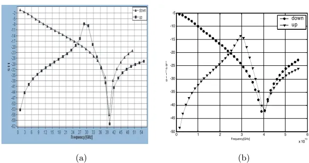
Figure 8. Simulation and calculation results of the return loss (S11)
in the up and down state position. (a) Simulation diagrams. (b)
Calculation diagrams.
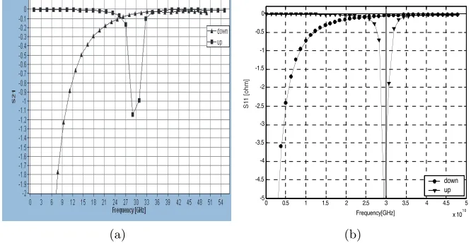
the first resonance frequency (30 GHz) in the up state position. Figure 9 shows simulation and calculation results of the insertion loss (S21) in the up and down state position. These diagrams show high insertion loss as a result of low impedance characteristic for the frequencies lower than fr(down) in the down state position. These diagrams also show maximum insertion loss as a result of minimum impedance at the first resonance frequency in the up state position.
0 0.5 1 1.5 2 2.5 3 3.5 4 4.5 5 x 10¹⁰ -5
-4.5 -4 -3.5 -3 -2.5 -2 -1.5 -1 -0.5 0
Frequency[GHz]
down up
S1
1 [ohm]
(a) (b)
Figure 9. Simulation results of the insertion loss (S11) in the up and down state position. (a) Simulation diagrams. (b) Calculation diagrams.
0 0.5 1 1.5 2 2.5 3 3.5 4 4.5 5
x 1010
-60 -40 -20 0 20 40 60 80
down up
Frequency[GHz]
Phase shift [degree]
(a) (b)
0 1 2 2.63 3 4 5 x 10¹⁰ -40
-35 -30 -25 -20 -15 -10 -5 0
Frequency[GHz]
S
11[
dB
]
down up
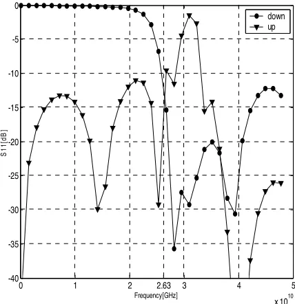
Figure 11. Return loss (S11) diagrams of 21 cascaded cells in the up and down state position (calculated using MATLAB).
difference between up and down state position. It is seen,that fr1(up) is a critical point and the sign of the phase changes from negative in the frequencies lower thanfr1(up)to positive for the frequencies higher thanfr1(up).
Mechanical behavior of the structure is simulated using intellisuite software. Simulation results show the actuation voltage of 39 volt. Considering the equation (12) the calculation results in a actuation 28 volt. This equation is based on parallel plates. MEMS bridge is one of the plates. When the actuation voltage is applied,the bridge bends. Beam bending causes unequally electrostatic force that is not considered in the equation.
6. MULTI-CELL DESIGN CONSIDERATIONS
The ABCD matrix is defined so that pairs can be cascaded by
simple multiplication and equations. For multi-cell structure shown
in Figure 4,each cell is represented by an ABCD matrix and the
cells are combined using ABCD matrices. The cells are cascaded by multiplication working from right to left. At the end of the calculation,
be converted to measurable S-parameters using equations (18) and (27). For the proposed Ka-band MEMS phase shifter,one bit MEMS phase shifter containing 21 cascaded cells is calculated using MATLAB software. The calculated S-parameters and phase diagrams in the up and down state positions are shown in Figures 11,12 and 13. From these figures it can be seen that the acceptable frequency range for the design is between 26 GHz and 27 GHz. and the optimum point for
S11, S21 and phase shift is around 26.3 GHz. The return loss between 26 GHz and 27 GHz is better than −10 dB. Considering the desired frequency and equations (32) and (34),the transmission line resistance is Rt = 340 Ω/m. Finally,the loss can be calculated using equation (33).
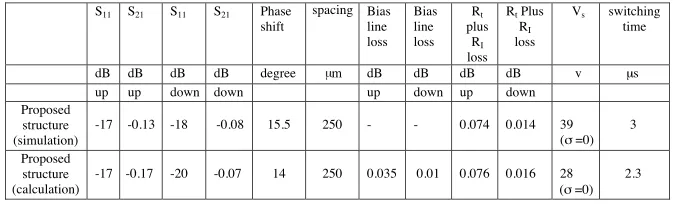
Table 2. Calculation and simulation results of the unit cell at 26.3 GHz.
S11 S21 S11 S21 Phase
shift
spacing Bias line loss
Bias line loss
Rt
plus RI
loss Rt Plus
RI
loss
Vs switching
time
dB dB dB dB degree m dB dB dB dB v µs up up down down up down up down
Proposed structure (simulation)
-17 -0.13 -18 -0.08 15.5 250 - - 0.074 0.014 39 (σ=0)
3
Proposed structure (calculation)
-17 -0.17 -20 -0.07 14 250 0.035 0.01 0.076 0.016 28 2.3 (σ=0)
µ
Table 3. Calculation results of 21 cells with the phase shift of 270◦ at 26.3 GHz.
S11(up) S21(up) S11(down) S21(down) Phase shift Length
dB dB dB dB Degree mm
Proposed structure (calculation)
-16 -1.65 -12.5 -1.6 265 5.25
Capacitive
type[8] - - -11.5 -2.1 270 8.4
Table 2 shows calculation and simulation results of the unit cell at 26.3 GHz. This table also compares obtained results with the unit cell of capacitive type.
0 1 2 2.63 3 4 5
x 1010
-50 -40 -30 -20 -10
-1.50
Frequency[GHz]
S
2
1[
dB
]
down up
Figure 12. Insertion loss (S21) diagrams of 21 cascaded cells in the up and down state position (calculated using MATLAB).
0 1 2 2.63 3 4 5
x 1010
-200 -150 -100 -50 0 50 100 150 200
down up
Frequency[GHz]
Phase shift [degree]
7. CONCLUSION
This paper presented small size and low loss Ka-band distributed
MEMS phase shifter. The concept of MEMS phase shifter using
inductor was introduced and governing equations on impedance,loss and scattering parameters were derived. For a multi-cell containing 21 cells at 26.3 GHz,the Un-actuated calculation resulted in a reflection coefficient −16 dB,and an insertion loss of −1.65 dB. The actuated calculation resulted in a reflection coefficient −12.5 dB,and an insertion loss of−1.6 dB. The phase shift for the whole structure was 265 degree. The spacing in the proposed structures wasS= 250×10−6. The length and the loss per bit with the phase shift of 265◦ were decreased by 37.5 percent and 21 percent respectively.
ACKNOWLEDGMENT
This work has been supported by the Malaysian Ministry of Science, Technology and innovation under the project title “MEMS devices and sensing microstructures 03-02-02-0015-SR0003/07-01”.
REFERENCES
1. Wang,Z.,B. Yan,R. M. Xu,and Y. Guo,“Design of a Ku band six bit phase shifter using periodically loaded-line and switched-line with loaded-switched-line,” Progress In Electromagnetics Research, PIER 76,369–379,2007.
2. Akdagli,A.,K. Guney,and B. Babayigit,“Clonal selection algorithm for design of reconfigurable antenna array with discrete phase shifters,” Journal of Electromagnetic Waves and
Applications,Vol. 21,No. 2,215–227,2007.
3. Barker,N. S. and G. M. Rebeiz,“Distributed MEMS true-time delay phase shifters and wide-band switches,” IEEE Trans.
Microwave Theory and Tech.,Vol. 46,No. 1,1881–1890,1998.
4. Borgioli,A.,Y. Liu,A. S. Nagra,and R. A. York,“Low-loss
distributed MEMS phase shifter,”IEEE Microwave Guided Wave
Lett.,Vol. 10,7–9,2000.
5. Hayden,J. S. and G. M. Rebeiz,“2-bit MEMS distributed X-band phase shifters,”IEEE Microwave Guided Wave Lett.,Vol. 10,540– 542,2000.
6. Liu,Y.,A. Borgioli,A. S. Nagra,and R. A. York,“K-band 3-bit low-loss distributed MEMS phase shifter,” IEEE Microwave
7. Hayden,J. S.,A. Makczewski,J. Kleber,C. L. Goldsmith, and G. M. Rebeiz,“2 and 4-bit DC-18 GHz microstrip MEMS distributed phase shifters,” IEEE MTT-S Int. Microwave Symp. Dig.,219–222,May 2001.
8. Pillans,B.,S. Eshelman,A. Malczewski,J. Ehmke,and
C. L. Goldsmith,“Ka-band RF MEMS phase shifters,” IEEE
Microwave Guided Wave Lett.,Vol. 9,520–522,1999.
9. Kim,M.,J. B. Hacker,R. E. Mihailovich,and J. F. DeNatale, “A DC-to-40 GHz four-bit RF MEMS true-time delay network,”
IEEE Microwave Wireless Comp. Lett.,Vol. 11,56–58,2001.
10. Hayden,J. S. and G. M. Rebeiz,“Very low-loss distributed X-band and Ka-band MEMS phase shifters using metal-air-metal capacitors,”IEEE Trans. on Microwave Theory and Tech., Vol. 51,No. 1,309–314,2003.
11. Hung,J.-J.,L. Dussopt,and G. M. Rebeiz,“Distributed 2- and
3-bit W-band MEMS phase shifters on glass substrates,” IEEE
Trans. on Microwave Theory and Tech.,Vol. 52,No. 2,600–606,
2004.
12. Hayden,J. S.,“High-performance digital X-band and Ka-band distributed MEMS phase shifters,” Ph.D. thesis, University of Michigan,Ann Arbor,2002.
13. Barker,N. S.,“Distributed MEMS transmission lines,” Ph.D.
thesis,University of Michigan,Ann Arbor,1999.
14. Rao,S. S.,Mechanical Vibrations,Addison-Wesley Publishing
Company,1995.
15. Wolff,E. A.,Microwave Engineering and Systems Applications,
John Wiley & Sons Publication,1988.
16. Pozar,D. M.,Microwave Engineering,Addison-Wesley Publishing Company,Reading,MA,1990.
17. Hoffmann,R. K.,Handbook of Microwave Integrated Circuits,
Artech House,Norwood,MA,1987.
18. Rebeiz,G. M.,RF MEMS Theory Design and Technology,John
Wiley & Sons Publication,2003.