INSTRUCTION MANUAL MODEL 304
GTSe
l
, GRANT TECHNOLOGY SYSTEMS CORPORATION
INSTRUCTION MANUAL
MODEL 304
SERIAL I/O BOARD
MODEL 304
SERIAL I/O BOARD
TABLE OF CONTENTS
Description
Features General
Specifications Q-Bus Interface
Interrupt Logic Console Channel UART
Control & Status Registers
Data Registers Error Registers EIA Circuit
Baud Rate Generator
Operation Modes
Factory Configuration Setting the Base Address Setting the Vector Address Setting the Interrupt Level Enabling the Console
System Halt or Reboot Setting the Baud Rate
Setting the Serial Data Format Setting the Line Discipline Reader Run Pulse
Serial Interface
Connector Description
Line Discipline, Cable Length &
Data Rates
FEATURES
*
*
*
*
*
*
Direct Replacement for DLV11-J Serial I/O Board
Totally Compatible with DEC Software
All Standard DEC Features
Each Port Independently Configured for Either EIA RS-232, RS-422, or RS-423
Four Level Vector Interrupt Structure, Ideal for Multi-User Applications
Channel 3 can be Independently Configured as System Console
GENERAL
The Model 304 is a four channel serial I/O port for interfacing
DEC's Q-bus to asynchronous serial data channels. The 304 is
a direct replacement for the DEC four channel Serial I/O Board
(Model DLV11-J). It is packaged on the standard 8.9" x 5.2"
DEC style dual width board and is electrically and mechanically compatible with DEC's LSI-II, 11/2, and 11/23 Microcomputer Series.
Each channel consists of a UART which receives and converts serial start, data, parity and stop bits to parallel data verifying proper code transmission, parity and stop bits. The UART's transmitter converts the computer's parallel data into serial form and automatically adds start, parity, and stop bits.
Each channel's data length can be configured for 7 or 8 bits. Parity is jumper selectable, odd or even, and parity checking
and generation can be inhibited. stop bits are jumper
selec-table; one or two.
The 304 can be used in a wide range of interface applications including printers, terminals, peripherals and remote data
acquisition systems. Each channel can operate at one of nine
jumper selectable data rates, from 150 to 38.4K baud, which
are generated by an on-board clock. The user may also
pro-vide an external clock.
The line characteristics of each channel can be jumper con-figured to operate in accordance with EIA standard RS-232,
RS-422, or RS-423. Twenty milliamp current loop operation is possible when used in conjunction with the DEC DLV11-KA.
'A unique feature of the 304 is the capability to support the
LSI 11/23 four level interrupt structure. Channel 3 may
also be configured as the system console, independent of the
other three channels. Special pins are provided on each
I/O connector which can be used to constantly assert the
data terminal ready lines of the peripheral, and each channel can also be configured to provide a pulse output to control a paper tape reader.
SPECIFICATIONS
Bus Interface
Data Characteristics
(Each Channel)
No. of Channels
Data Protocol
Baud Rates
Line Discipline
Data Bits
stop Bits
Parity
Addressing
Base Address Range
Console Address
Interrupts
Priority Level
Base Vector Range
Console Vector
Q-bus, DEC LSI-11, 11/2 &
11/23 compatible
4
Asynchronous serial
Jumper Selectable 150, 300, 600, 1.2K, 2.4K, 4.8K, 9.6K, 19.2K 38.4K, Ext.
Jumper Selectable EIA RS-232C, RS-422, or RS-423
Jumper Selectable 7 or 8
Jumper Selectable 1 or 2
Jumper Selectable Odd, Even, None
Jumper Selectable 7760008 to 777740 8
Jumper Selectable 777560 8 Channel 3 Only
Jumper Selectable LSI-11 & 11/2
Level 4, Jumper Selectable LSI-11/12 Level 4, 5, 6, or 7
Jumper Selectable 0 to 740 8
Mechanical & Environmental
Dimensions
Power Requirements
Bus Loading
Operating Temperature Range
Storage Temperature Range
Relative Humidity
Mating Connector
Q-BUS INTERFACE
DEC LSI-II standard 8.9" x 5.2" half quad board
5V @ 1 Amp, 12V @ .2 Amps
1.5 Std. AC/1 Std. DC Load
o
to 55°CTo 85% non-condensing
Amp #87133-5, Pin #87165-2
The Q-Bus Interface consists of address/data
trans-ceivers, an address comparator, console decode logic and I/O select and control logic.
During the addressing portion of a bus cycle, the Address/
Data transceivers are in the receive mode. Address lines
12 through 5, gated by bus line BBS7, are compared to the base address setting selected by the address selection
jumpers. When the correct address is asserted by the
pro-cessor, the comparator output (BDSEL) is asserted. This
in conjunction with the assertion of BSYNC is used by the Select and Control Logic (SCL) to select the appropriate on-board register for the remainder of the bus cycle.
If the processor is performing a read, then the BDIN line is decoded in conjunction with the SCL to enable the tri-state buffers of the selected register, place the bus trans-ceivers in their transmit mode, and then assert the BRPLY line.
If the processor is performing a write operation, then the register which is to be written to is selected during the Address/Data portion of the bus cycle and the BDOUT line is
used to clock the latches of the receiving register, and to assert BRPLY.
INTERRUPT LOGIC
The interrupt handling logic consists of interrupt request logic, a priority encoder, level circuit logic, arbitration control, and vector logic.
The interrupt request logic consists of eight latches; one
for each transmit or receive CSR. In order to generate an
---1
-~--l--:L ISAUO 1 0
: ~~~7l~~TOR J----=r
L ___ . ______ _
UART CONTROL STATUS LINES
:..~ I'
I
Ii!I
CONTROL ~l§I 18111 I
~::"',
J
,I
i Uk: ',~~~~ERS
••.."
~ITT!
§ 18I
'
CHOREC ,i8l ~ l i i~U8 ~ ~HtXMTj : 1
, l l i l l ' i ,!8 ! C[ : ~ eM 1 AEC i
~
U i I I I I I ' Ill' ..
§i
I'. !----l, '" "ctiliMr-j~'
. )W
~ .!./.J,J.+oui --ll-.J LJ . : I i i --~j ~ CH 2 REC : ' "
I
! I [ 0 : I I -- -
::--~--- ~. ,~-; ~~~
•i
i
U
II
AiibOESSOAT1 ..h2 :
TT1Trr--TTJ"
~~
,
8 ~ 8 x :<:ib c~. =x= D~D i ---, 141
r
'DORESS SELEC~ i . I II
~~
j
i o:....:E:=::J ! u-T i ' : ; CH 3 XMT !
._ ....• eo...
T~II"
'-~_:~_-_==--' - - ~I
i Ll-~~.~;:-~!L~RLl ,r---" I VEe i
-i CONSOL;-l
,SELECT '
l . JUMPERS ,J1
r
I [ -
,I
I I , II
I : ~J 'ECTOR L.OGIC1 ' r-=--~- I
I
~II :----~ i ,---~---~' ,~'~I iJ , __
~··t-T---·----I~lli~ I . ,.TERRUPT ~
-1
z ~ REQUEST a IRQ L~ PJilORITYU "'I __ :~~ _ _ ~-I--l ENCODER
_ I _~d:~~SET
J
l f 'RO SELECT & I : INTERRUPT -~---: I i _ .. _. ' CONTROt I A~BITRATlON ~-,: INTERRUPT• LOGIC I
I
8. OONTqoL lUO: LEVELI i LOGIC ~~-- - - SELtCT
-~-In'
I
!-ITi ---'
_nl_~
___--,--l;,l'-'--~U~:ST
, I , I .
1 ! j ~
I
f • ti~~I~ D D D
FUNCTIONAL BLOCK DIAGRAM
MODEL 304
~
i
~ a 8 (;~ ~! !
I
! FE.
HALT
~EBOOT
JUMPERS
~ ~ ~ !
enable bit (Bit 6) in either the transmit or receive CSR must be set, and second, the appropriate condition flag
must be set (Bit 7). These two logically anded signals
clock the flop. The outputs of all eight flops are fed
into the priority encoder. When the output of any flop
goes high, the priority encoder generates a master
inter-rupt request (IRQ). This signal is fed into the level
select logic which in turn asserts the appropriate BIRQ
lines. At the same time the arbitration logic monitors
the bus to determine if a device on a higher interrupt level
is requesting. If not, then when the interrupt grant signal
BIAKI is received,the appropriate vector as determined by the priority encoder is placed on the bus, and if more than one channel is requesting, the channel of highest priority is cleared leaving the lower priority requests pending. Table 1 gives the priority level of each channel.
Channel Level Vector Offset
Channel 0 Receive 0 Highest Priority Base Vector +0
Channel 1 Receive 1 Base Vector +10
Channel 2 Receive 2 Base Vector +20
Channel 3 Receive 3 Base Vector +30
Channel 0 Transmit 4 Base Vector +4
Channel 1 Transmit 5 Base Vector +14
Channel 2 Transmit 6 Base Vector +24
Channel 3 Transmit 7 Lowest Priority Base Vector +34
TABLE 1
CONSOLE CHANNEL
When the console enable jumper is installed, Channel 3 will respond to the address of 1775608' and the receiver will
always have a vector address of 608' The transmitter vector
will be 64 8 , The console mode of operation is independent of
the board's base address.
UART
Each channel consists of a Universal Asynchronous Receiver Transmitter (UART) which receives and converts serial data, parity and stop bits to parallel data verifying proper code
transmission, parity and stop bits. If a transmission error
register which is read when the receive data register is
read. Upon receiving the last stop bit, the receiver full
flag is set (Bit 7 of the receive CSR). If the receiver
interrupt enable bit is set (Bit 6), then the receiver full flag will generate an interrupt request.
The UART's transmitter converts the computer's parallel data into a serial format and automatically adds start,
parity, and stop bits. When the transmitter buffer is
ready to receive a byte of data for transmission, the
trans-mitter ready flag is set (Bit 7 of the transtrans-mitter CSR). If
the transmitter interrupt enable bit is set (Bit 6), then the transmitter ready flag will generate an interrupt.
CONTROL STATUS REGISTER (CSR)
Each channel contains a 16 bit receiver CSR and a 16 bit
transmitter CSR. Bit 7 is a read only bit used as a status
flag and Bit 6 is a read/write bit used to enable an interrupt request when Bit 7 gets set.
Bit 7 of the receiver CSR is used to indicate that the
receiver contains new data. Bit 7 is cleared by reading the
receiver's data register or by a software reset. When Bit 6
is set, an interrupt request is generated when Bit 7 is set.
Bit
0
of the receiver CSR is used to transmit a reader runpulse. This bit is a write only bit and always reads zero.
Bit 7 of the transmitter CSR, when set, indicates the trans-mitter buffer is empty and ready to transmit new data.
Setting Bit 6 will generate an interrupt whenever Bit 7 is set.
Bit
0,
when set, will transmit a continuous break.All unused CSR bits in both the transmitter and receiver CSR's will always read zero.
DATA REGISTERS
Each channel contains a Receiver Data Register (ROR) and a
Transmitter Data Register (TOR). When data is received,
i t is placed in the ROR and Bit 7 of the Receiver CSR is
set. The received data is obtained by reading this register
Data to be transmitted is written to the TOR. This
auto-matically clears Bit 7 of the Transmitter CSR. Here the
data will remain until the transmitter is ready. The data
is then placed into the transmitter setting Bit 7.
ERROR REGISTERS
Each channel contains a 4 bit error register which is comprised of Bits 15 through 12 of the RDR.
Bit 12 is the Parity Error (PE) Bit. A "1" indicates the
receiver parity does not match the parity selected by the
format jumpers. The PE bit remains set until parity
matches on a succeeding character. When parity is inhibited,
this bit always reads zero.
Bit 13 is the Framing Error (FE) Bit. A "1" indicates the
first stop bit was invalid. The FE bit will stay set until
the next valid character's stop bit is received.
Bit 14 is the Overrun Error (DE) Bit. A "1" indicates that
the last character was not read from the RDR before a new
character was received. The DE is reset at the next
character's stop if Bit 7 of the Receive CSR cleared.
Bit 15 is the Error Flag (EF) and is the logical "oring"
of the PE, FE, and DE bits. The setting of any error bit
will set this bit.
EIA CIRCUIT
The EIA circuit for each channel consists of a differential line driver, line receiver, and a single ended line driver. Through the use of wire wrap jumpers, each channel can be configured to operate as RS-232C, RS-422, or RS-423.
Channels operating as RS-232C or RS-423 will configure the differential line receiver to operate single ended and
utilize the single ended line driver. The slew rates of the
line drivers are controlled by changing external resistors.
Channels which operate as RS-422 configure the differential line receiver for differential operation by adding a 100 ohm termination resistor, and utilize the differential line
driver.
BAUD RATE GENERATOR
The baud rate generator consists of a crystal oscillator
and divider. The oscillator base frequency is 4.1952 MHz
which is divided to yield the nine baud rate clocks. Each
MODES OF OPERATION
Each channel of the 304 can operate in various line
disci-plines, data formats, and baud rates. The base address can
be set so that the board can reside in any I/O page
loca-tion. The vector can also be set to any address from 08to
774S' and the interrupt level can be set to 4, 5, 6, or 7. All of these operation modes are configured by setting wire
wrap jumpers. Table 2 is a summary of the jumper selectable
modes which the board can be configured to.
TABLE 2
Jumper Selectable Modes of Operation
Mode Description
*
Line Discipline*
Baud Rate*
Serial Data FormatBase Address
Vector Base Address
Console
Halt/Reboot on Break
Interrupt Level
*
Channel to Channel ConfigurableMode Selection
RS-232C, RS-422, or RS-423
150, 300, 600, 1200, 2400, 4S00, 9600, 19.2K, 3S.4K, External
Data Bits, 7 or S stop Bits, 1 or 2
Parity, Odd, Even, None
160000 S to 177740 8
o
to 7408Enable Channel 4 as System Console
Address CH 4 = 177560 S
Vector CH4
=
60 SChannel 3
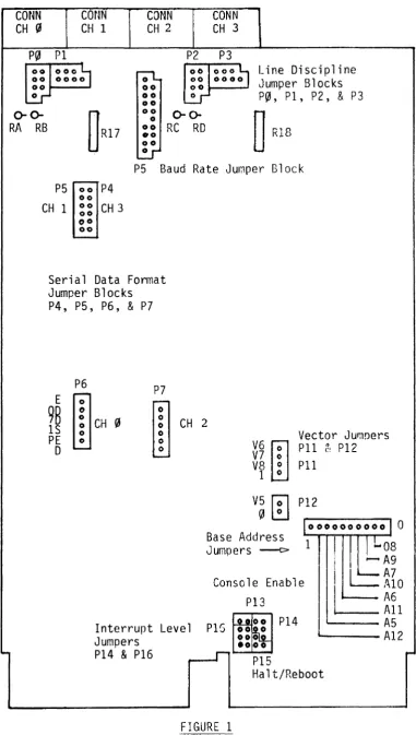
-CONN
CH
(IPlil
00 00 00
CONN
CH
1PI
0 0 0
!l
0 0 0 0CONN
CONN
CH 2
CH 3
P2 P3
00 oooL,
Line Discipline
: : 0 0 0 0
I
Jumper Blocks
~
00 00 00 0 0
~
PIil, PI, P2,
&
P3
0-0-OR!)
RA RB
P5
r-;;
P4
00 o 00 00 0 0 ~
o-cr
RC RD
DRIB
P5 Baud Rate Jumper Block
CH
1 ::CH
30 0 00
~
Serial Data Format
Jumper Blocks
P4, P5, P6,
&
P7
P6
Ern
98 :
CH
(IIS 0
PE
0D
P7
m
CH 2
V6 V7ill
0V8 0
1 0
Vector Jumpers
Pll f.! Pl2
Pll
V5
rol
P12!il
~,--_ _ _ _
-.
1000000000010
Base Address
I
Jumpers
- - c >I
I
1...08
-A9
W
1~ro
Console Enable
P13
Interrupt Level
Plr. ;) ~~o 00 0 0 P14000 A6
A11
~--A5 ~---A12Jumpers
P14
&
P16
~FIGURE 1
eooo
P15
Halt/Reboot
FACTORY CONFIGURA'l'ION
The Model 304 is shipped configured as follows:
TABLE 3
Base Address
Vector Base Address
CH3 Console Enabled
CH3 Halt on Break
*
Serial Data Format*
Line Discipline*
Baud RateInterrupt Level
*
All ChannelsSETTING THE BASE ADDRESS
Yes
Enabled
1 Stop Bit, 8 Data Bits, No Parity
RS-232C
9600
4 (LSI 11)
The 304's base address can be set to reside anywhere within
the I/O page. The location of the base address jumpers is found
on Figure 1. To change the board's base address requires
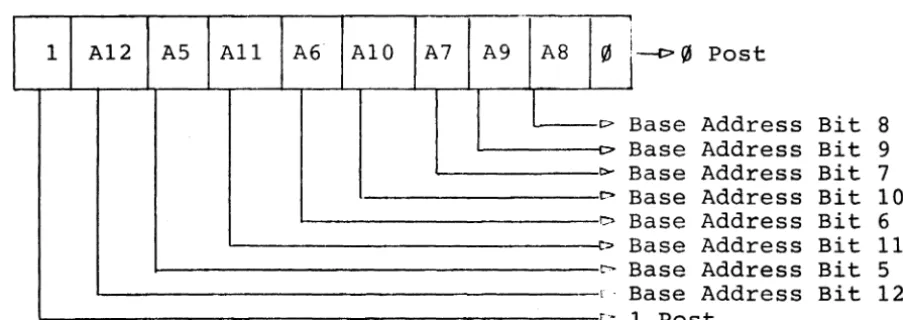
reconfiguring the base address jumpers. Figure 2 indicates
the base address jumper post arrangement. To change an
address bit from 0 to 1 or vice versa requires wire
wrapping that bit to the post labeled 0 or 1.
· 0
1 A12 AS All A6 A10 A7 A9 A8
FIGURE 2
Base Address Jumpers
0
[>
-
b0-t>
I> Co>
t>
1 0 r o.
,
,
j
----P (6 PostBase Address Bit 8
Base Address Bit 9
Base Address Bit 7 Base Address Bit 10
Base Address Bit 6
Base Address Bit 11 Base Address Bit S Base Address Bit 12
As an example, the factory configured base address is
176500S. To set the base address requires wire wrapping
A12, All, A10, A8, and A6 to 1 and A9, A7, and A5 to
O.
Refer to Table 4.
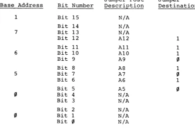
TABLE 4
Factory Configured Base Address
Jumper Post Jumper
Base Address Bit Number Description Destination
1 Bit 15 N/A
Bit 14 N/A
7 Bit 13 N/A
Bit 12 A12 1
Bit 11 All 1
6 Bit 10 A10 1
Bit 9 A9 ~
Bit
a
AS 15 Bit 7 A7 ~
Bit 6 A6 1
Bit 5 A5 ~
~ Bit 4 N/A
Bit 3 N/A
Bit 2 N/A
Bit 1 N/A
Bit ~ N/A
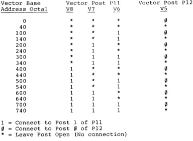
SETTING THE VECTOR ADDRESS
The 304's vector address can be set from 0 to 740S. The
location of the vector selection jumpers are found by
referring to Figure 1. Wire wrapping jumper posts V6, V7
or V8 to Post 1 will cause these vector bits to read as 1.
No connection will cause these bits to read
o.
Connecting jumper post V5 to 0 will cause vector Bit 5 to
read
O.
No connection of V5 will cause vector Bit 5 toread as 1.
As an example, the factory configured vector is 300 S . This
requires leaving Post
va
open, connecting V6 and V7 to Post 1and connecting V5 to Post
o.
Table 5 is a vector configuration guide. Vector Posts V6,
Post vS should never be connected to Post 1. THIS WILL RESULT IN AN ERRONEOUS VECTOR.
TABLE 5
Vector Selection Jump'e~~
Vector Base Vector Post P 1] Vector Post
Address Octal va V7 V6 V5
0
*
*
*
0
40
*
*
*
*
100
*
*
10
140
*
*
1*
200
*
1*
0
240
*
1*
*
300
*
1 10
340
*
1 1*
400 1
*
*
0
440 1
*
*
*
500 1
*
10
540 1
*
1*
600 1 1
*
0
640 1 1
*
*
700 1 1 1
0
740 1 1 1
*
1
=
Connect to Post 1 of pll0
=
Connect to Posto
of p12*
=
Leave Post Open (No connection)SETTING THE INTERRUPT LEVEL
pl2
The 304 can fully support the 11/23 multi-level interrupt
structure. To do so requires that the 304 assert the
appropriate interrupt request lines (BIRQ4, BIRQS, BIRQ6 and BIRQ7) and monitor interrupt request lines of higher
priority. Jumper post block P14 (Fig. 1) is used to select
which interrupt request lines are to be asserted, and jumper post block P16 (Fig. 1) is used to select which interrupt request lines are monitored.
The 304 is factory configured to support systems which do not support a multi-level interrupt structure, which means that its priority level is strictly a function of its
electrical locations relative to the processor. To change
TABLE 6
Interrupt Level Configuration Jumpers
Interrupt Level Request Level Monitor
Level Jumpers Pl4 Jumpers P16
Rs R6 R7 LMI LM(&l
*
11/2 G G G P P
4 G G G 05 06
5 IR G G P 06
6 G IR G P 07
7 G IR IR P P
*
This configuration is set at the factory and mustbe used in systems which do not support the multi-level interrupt.
P13 P14
COE
II
IR RsLMI Qs G R6
LMI1l Q6
R~
P 07 C H
P16 P1s
FIGURE 3
ENABLING THE CONSOLE
Channel 3 can be enabled as the system console independent
of the base and vector address settings. To enable this
option requires installing jumper P13. To disable this
option requires rerrloving jumper p13. Refer to Figure 1.
When the console is enabled, Channel 3 will respond to addresses 1775608 to 177566 and will output a vector of 60 and 64 for the receiver and transmitter interrupts,
respectively. Caution should be employed when the console
is enabled so as not to set the base address equal to 177540 or a conflict will exist between Channel 2 and Channel 3.
By disabling the console, (remove jumper P13) and setting the board's base address equal to 177540 and setting the
vector equal to 40 8 , Channel 2 will act and respond as the
system console.
SYSTEM HALT OR REBOOT
Any device con~unicating through Channel 3 can generate a
system Halt or power up initialization by outputting a "BREAK".
To generate a system Halt on BREAK requires installing
a jumper at P15 (Figure 3) from C to H. To generate a
power fail reset, connect C to R. Refer to Figure 1 for
jumper block P15's location.
SETTING THE BAUD RATE
Each channel of the 304 can con~unicate at one of nine
jumper selectable baud rates or at an externally provided
clock rate. Table 7 lists the baud rates and the jumper
post identification letter. Figure 4 details the baud rate
jumper block, the location of which can be found by referring to Figure 1.
Setting a channel to operate at a particular baud rate requires jumpering the appropriate pin whose letter repre-sent the desired baud rate to the pin labeled for that channel (Refer to Figure 4).
As an example, the 304 is shipped from the factory with
all 4 channels set to operate at 9600 baud. The baud rate
jumper post C is connected to jumper posts CH~, CH1, CH2,
TABLE 7
Baud Rate Jumper Identification
Baud Rate
150 300 600 1200 2400 4800 9600 19.2K 38.4K 38.4K 19.2K 9600 4800 2400 1200 600 300
150 Baud
FIGURE 4
Letter I H G F E D C B A A
B CH0 Channel 0
C CKIJ Ext. Clock
D CH1 Channel 1
E CK1 Ext. Clock
CH2 Channel 2
F CK2 Ext. Clock
G CH3 Channel 3
H CK3 Ext. Clock
I
Baud Rate Jumper Block Detail P5
SETTING THE SERIAL DATA FORMAT
Channel
Channel
Channel
Channel
Each channel of the 304 can be configured to operate in the following data formats:
7 or 8 Data Bits 1 or 2 stop Bits
Odd, Even, or with No Parity
0
1
2
Jumper posts P6, PS, P7, and P4 (Figure 1) are used to set
the data formats of Channels ~ through 3 respectively. The
jumper configuration of the various options are illustrated
in Table 8. As an example, the 304 is configured for 8
data bits, 1 stop bit, and no parity. This requires
jumper-ing PE and 7D to E and jumperjumper-ing IS to E. When parity is
not enabled, the odd/even parity post has no effect but
must be jumpered to either E or D. Figure 5 illustrates
the format jumper arrangement.
TABLE 8
Format Jumper Configuration Guide
Format Option Jumper Configuration
8 Data Bits 7D to D
7 Data Bits 7D to E
2 Stop Bits IS to D
1 Stop Bit IS to E
No Parity PE to D
Parity PD to E
Even Parity OD to D
Odd Parity OD to E
E Enable
OD Odd Parity/Even Parity
7D 7 Data Bits/8 Data Bits
IS 1 stop Bit/2 Stop Bits
PE Parity/No Parity
D Disable
FIGURE S
Serial Data Format Jumper Block Detail
SETTING THE LINE DISCIPLINE
Each channel of the 304 can operate in anyone of the following EIA line disciplines:
RS-232C RS-422 RS-423
The jumper blocks used to configure Channels ~ through
3 are PO, PI, P2, and P3 (Figure 1), respectively. Table
9 illustrates the jumper configuration to set up each
channel. As an example, the 304 is shipped from the factory
with each channel set up to operate in RS-232C. This
requires jumpering S+ to 1+ and S- to I-. Figure 6
illustrates the layout of the line discipline jumper blocks.
TABLE 9
Line Discipline Jumper Configuration
Line Jumper
Discipline Configuration
RS-232C I+ to S+, I- to
S-*
RS-422 I+ to D+, I- toD-RS-423 I+ to S+, I- to
S-*
Add 100 ohm termination resistor, (RA, RB, RC , RD)I- D- P
S- S+ I+ D+
FIGURE 6
Line Discipline Jumper Block Layout
(PO, Pl, P2, & P3)
When a channel is set up to operate in RS-422, a 100 ohm termination resistor must be installed at the input of
the differential receiver. Table 10 lists the channel
number and resistor name.
TABLE 10
RS-422 Resistor Installation Guide
Channel
0
Install a 100 ohm resistor at RAChannel 1 Install a 100 ohm resistor at RB
Channel 2 Install a 100 ohm resistor at RC
Channel 3 Install a 100 ohm resistor at RD
During data communication over long data leads i t may be necessary to change the rise and fall times of the single ended line drivers used in RS-423 to reduce line
reflections and the potential of data errors. R17 controls
the transition time for Channels
0
and 1 and R18 controlsChannels 2 and 3. The resistor installed at the factory is
a 22K which sets the transition time at 2.2ps. Table 11 is
a list of recommended resistor values as a function of baud rate which should be installed if line reflections become a problem.
TABLE 11
RS-423 Slew Rate Resistor Values
Resistor Nominal
Baud Rate Value in Ohms Transition Times
150 1 Megohm 100 usec
300 1 Megohm 100 }.lsec
600 1 Megohm 100
.u
sec1200 820K Ohm 82 jlsec
2400 430K Ohm 43 )lsec
4800 200K Ohm 20 )lsec
9600 lOOK Ohm 10 j.lsec
19.2K 51K Ohm 5.1 )lsec
READER RUN PULSE
The reader run pulse is used to control a paper tape reader. To use this control requires connecting P to 'I- at the appropriate line discipline jumper block
(Figure 1). Figure 6 illustrates the location of this jumper with the line discipline jumper block.
SERIAL INTERFACE
Figure 1 illustrates the connector location for each channel.
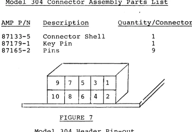
CONNECTOR DESCRIPTION
Each channel is interfaced through a 10 pin header. Figure
7 illustrates the pin-out location. The mating connector
is manufactured by AMP, Inc. Table 12 lists the parts
which are required to assemble the mating connector. The
connector may be obtained through AMP, AMP distributors, or GTSC.
TABLE 12
Model 304 Connector Assembly Parts List
AMP PIN
87133-5 87179-1 87165-2
Description
Connector Shell Key Pin
Pins
/
9 7 5 3
10 8 6 4
FIGURE 7 1
2
Quantity/Connector
/
/
-V
1
1
9
Model 304 Header Pin-out
The pin-out description of each header is as follows:
Pin No.
1 2 3 4 5 6 7 8 9 10 Description
Clock I/O Signal Ground Transmit Data + Transmit Data -Signal Ground Key (No Pin) Receive Data -Receive Data + Signal Ground +12 Volts (Fused)
When a channel is configured for RS-232C or RS-423, Pin 7 must
be externally tied to signal ground. This is typically done by
LINE DISCIPLINE, CABLE LENGTH & DATA RATES
The two basic methods for electronic communications are single ended transmission and differential transmission. RS-232 was developed for single ended transmission over
short distances at slow data rates. RS-423 extends the
maximum data rate and cable length beyond that of RS-232. It also provides for wave shaping dependent on data rate and wire length to control reflections.
For communications over long distances, differential transmissions (RS-422) should be used to nullify effects of ground shifts and noise signals which appear as common
mode. Table 13 lists the maximum recommended cable length
and data rates for each line discipline.
TABLE 13
Key Aspects of RS-232,
Specification
Mode of Operation
No. of Drivers &
Receivers allowed on one line
Maximum Cable Length
Maximum Data Rate
RS-423 & RS-422
RS-232C
Single-ended
1 Driver 1 Receiver
50 feet
20 kb/s
21
RS-423
Single-ended
RS-422
Differential
1 Driver 1 Driver
10 Receivers 10 Receivers
4000 feet 4000 feet
PROGRAMMING
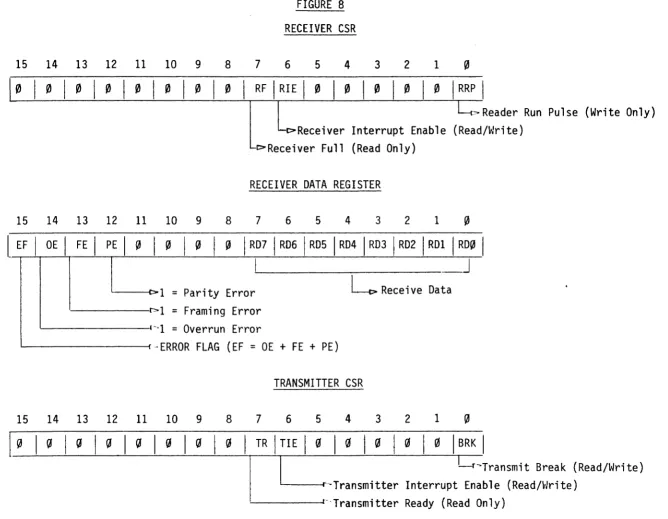
Figure 8 illustrates the functions of the four 16 bit
registers which comprise each channel. Thus, the Model
304 occupies 16 contiguous blocks in the I/O page
*
The registers which make up each channel are:
Receiver Control Status Register (RCSR)
Receiver Data Register (RDR)
Transmitter Control Status Register (TCSR)
Transmitter Data Register (TOR)
Table 14 illustrates the relationship between each
channel's registers and the base address. When the
con-sole is enabled, any attempt to address Channel 3
through an address other than the console address will cause a bus time out error.
Testing Bit 7 of the RCSR is used to indicate that the
UART has received new data. Reading the RDR will clear
Bit 7. Setting Bit 6 of the RCSR will enable the
receiver interrupts. When Bit 7 is set, an interrupt will
be generated.
Bit
S
of the RCSR is used to generate the reader run pulseby setting this write only bit. This action will also
clear Bit 7 of the RCSR.
Bits
S
through 7 of the RDR contain the data received bythe UART. Bits 12 through 15 indicate any errors which
have occurred during the reception of data.
Bit 7 of the TCSR indicates the status of the transmitter. When this bit is set, the transmitter is ready to receive
a new byte of data for transmission. When this bit is
cleared (Bit 7
=
S),
the transmitter is busy and no attemptto write the data to the TDR should be made. Setting Bit 6
of the TCSR will allow interrupts to be generated when Bit 7 is set.
Bit ~ of the TCSR is a read/write bit used to transmit a
continuous break. A "1" written to Bit ~ will transmit a
break (continuous ~), a zero clears the break transmission.
*
This only holds true if Channel 3 is not configured asthe console.
Data which is to be transmitted is written to the TOR, but only if Bit 7 of the TCSR is set.
Table 15 lists the relationship between the vector jumper
settings and each channel. Note, Channel 3's vector is
that of the console when the console is enabled.
Table 16 illustrates the register and vector address when Channel 3 is configured as the system console.
TABLE 14
Register Address Offset
Register Description Base Address Offset (Octal)
Channel (6 Receiver CSR Base Address +0
Channel (6 Receiver Data Register Base Address +2
Channel (6 Transmitter CSR Base Address +4
Channel (6 Transmitter Data Register Base Address +6
Channel 1 Receiver CSR Base Address +10
Channel 1 Receiver Data Register Base Address +12
Channel 1 Transmitter CSR Base Address +14
Channel 1 Transmitter Data Register Base Address +16
Channel 2 Receiver CSR Base Address +20
Channel 2 Receiver Data Register Base Address +22
Channel 2 Transmitter CSR Base Address +24
Channel 2 Transmitter Data Register Base Address +26
Channel 3 Receiver CSR Base Address +30
Channel 3 Receiver Data Register Base Address +32
Channel 3 Transmitter CSR Base Address +34
Channel 3 Transmitter Data Register Base Address +36
TABLE 15
Vector Address Offset
Interrupt Request Vector Base
Description Address Offset
Channel
!3
Receive!3
Channel (6 Transmit 4
Channel 1 Receive 10
Channel 1 Transmit 14
Channel 2 Receive 20
Channel 2 Transmit 24
Channel 3 Receive 30
TABLE 16
Console Register & Vector Addresses
When Console Option is Enabled
Channel 3
Register Description Register Address
Receiver CSR 17756°8
Receiver Data Register 177562 8
Transmitter CSR 177564 8
Transmitter Data Register 177566 8
Receiver Interrupt Vector Address
Transmitter Interrupt Vector Address
15
14
13
12
11
10
9~10101010101~
15
14
13
12
11
10
9
I
EF
I
OE
I
FE
I
PE
I
0
I
~
I
0
~
15
14
13
12
11
10
98 7
FIGURE 8
RECEIVER CSR
6 5 4 3 2 1 ~
o
I
RF
I
RIE
I
0
o o o o
I
RRP
I
~Reader
Run Pulse (Write Only)
Receiver Interrupt Enable (Read/Write)
Receiver Full (Read Only)
RECEIVER DATA REGISTER
8
7
6 5 4 3 2 1
~~
I
RD7
I
RD6
I
RD5
I
RD4
I
RD3
I
RD2 'RDI
I
RD0
I
_J
)
TRANSMITTER CSR
8 7 6 5 4 3 2 1
o
[!.-,
(JI
(JI
(JI
(JI
(JI
(JI
(JI
TR
I
TI EI
(II
(II
(II
(II
(II
BRK ,
.
I
I
l--r'Transmit Break (Read/Write)
TRANSMIT DATA REGISTER
15
14
13
12
11
10
9
8
7
6
5
4
3
2
1
~I
~
I~
I~
I~
I~
I~
I~
I~
ITD71 TD61 TD51 TD41 TD31 TD21 TDI
ITD~
II
.
I
~
=
Always Reads
~'----~t>
Transmit Data
FIGURE
8(Cont.)
~vARRANTY
Grant Technology Systems Corporation warrants that its products, except software, will be free from defects in workmanship or material under normal use and service. GTSC under this warranty will, at its option, replace or repair without charge at its plant any products manu-factured by GTSC.
Freight, insurance, and other charges incurred in re-turning the product to GTSC will be paid by the customer.
The terms of this warranty are 90 days from the original
date of shipment. The warranty provisions do not extend
to products which have been repaired or altered without prior written GTSC approval, or to products which became defective due to accident or to the customer's improper installation, application or maintenance.
This warranty is in lieu of any other warranty, that is expressed or implied, including warranties of
merchantabil-ity and fitness for use. GTSC reserves the right to make
any changes in the design or construction of its products at any time without incurring any obligation to make any changes to products previously delivered.
GTSC neither assumes nor authorizes any other person to assume for i t any other liability in connection with the sales, installation or use of its products.
GTSC shall have no liability for incidental or consequential damages of any kind arising out of the sale, installation, or use of its products.