Abstract—A particle detection chain based on CMOS-SOI VCO circuit is presented. The solution is used for the recognition and the tracking of a given particle at circuit level. TCAD simulation of the detector has been performed on a 3x3 matrix of diodes based detector for particles recognition and tracking. The current response of the detector has been used for a case study in order to determine the ability of the chain to recognize an alpha particle crossing a 3x3 detection cell. The detection limit of the proposed solution is investigated and discussed in this paper.
Index Terms— VCO, particle detector, TCAD simulation
I. INTRODUCTION
EMICONDUCTOR radiation detectors can be classified into
several categories, depending on the application field and the particles to be detected. These detectors, also called solid-state detectors, are based on charge collection and amplification, with the help of a semiconductor volume such as a p-n junction. They exhibit several advantages in comparison with other types of detectors such as gas-filled counters. For instance, they usually offer faster charge-collection times which provide the ability to process higher counting rates. An other advantage is their compactness which allows the measurement of intensity variations over small distances improving the measurement resolution. When a high detector sensitivity is required, a pixel organization including several sensors could be used and will be investigated in this work.
The signal generated by the sensor has to be conditioned in order to allow particles counting and/or recognition. Most of the existing conditioning chains are based on a direct reading of the detected currents created by the crossing of an ionizing particle through the matter. When an embedded reading system is necessary, this solution could not be suitable for the detection of low energy particles where the current signature
Manuscript received June 1st, 2017.
K. Coulié, W. Rahajandraibe, H. Aziza and R. Vauché are with Aix-Marseille University, CNRS and University of Toulon, IM2NP UMR 7334, Marseille France. Gilles Micolau is with Université d’Avignon, UMR 1114 EMMAH (INRA-UAPV), Avignon, France
could be a narrow pulse with a duration of few nanoseconds. Indeed, the readout chain must ensure sufficiently high resolution (optimized Signal-to-Noise-Ratio) for an appropriate post-processing. Moreover, a reading amplifier exhibiting a fast response time is required which means a higher current consumption and complex circuit implementation. Designing high precision, low-power wideband amplifier is a critical issue. As a consequence, most practical detectors are based on direct reading of the detected currents using Charge Sensitive Amplifiers (CSA) [1]. In this case, the circuit delivers a limited amount of information on the actual current shape. Then no information about the electrical signature of the particles is available. In applications such as gas prospection or medical therapy, the characteristics of the electrical signature of the particles must be known. Moreover, the knowledge of the generated current shape at the output of the detector allows easier post processing of the signal
In this context, a new approach based on the use of a ring oscillator was developed with an innovative conditioning method. This new approach is based on the reading of the information related to indirect output parameters of the detection chain signal (i.e. phase and frequency), instead of directly measuring the current from the sensor. This solution is interesting since it avoids most of the design problems described upper. Then, the information is extracted by correlating the initial oscillation signal of the system with the oscillating signal after the particle has passed the detector. To be able to make a diagnosis, the requirement is then to link the output information (i.e. phase and frequency of the oscillating signal) to the input information (current stimuli). The conditioning circuit has been implemented in 130-nm CMOS SOI (Silicon on Insulator) technology. The circuit has been designed at transistor level with transient simulation performed in Cadence Virtuoso platform.
In the second section of this paper, the context of this work is presented. The third section is dedicated to the VCO (Voltage Controlled Oscillator) presentation. Part IV deals with the VCO detection limits followed by a case study of a particle crossing a matrix of detectors (part V). The last section concludes the paper.
Detection limit of a VCO based detection
chain dedicated to particles recognition and
tracking
K. Coulié, W. Rahajandraibe, H. Aziza, G. Micolau, R. Vauché
II. CONTEXT OF THE WORK
From the late 1970s, high failure rates, due to alpha particles and mainly inducing a financial loss and recall of products, had serious consequences for several semiconductor manufacturers like Xilinx [2]. With the decreasing of the supply voltage and of the node capacitances, the Soft Error Rate (SER) due to alpha particles presents yet a major reliability concern to logic processors because of the critical charge decreasing. Solutions which limit alpha contamination exist but are often costly. For example, packaging alternatives such as a lid coat or flip-chip strongly influence the alpha induced SER. The use of 10B in the process can also greatly influence the SER by enhancing the alpha particle contribution. For a long time, fast neutrons were considered as the main danger for atmospheric applications but nowadays the alpha SER can be comparable to that of fast neutron induced SER [3-4]. To remain reliable, the nanoelectronic devices and systems must take into account upsets due to the transitory errors induced by alpha from radioactive contamination, and ideally, be hardened the best possible. As a consequence, one of the major issues for nanoelectronic companies is today to include/understand the phenomena related to the radioactive contamination in materials in order to prevent, detect, and analyze them.
Concerning medical application, a first clinical study reported in 1998 [5] has shown that cosmic neutron radiation could induce Single Event Upsets (SEU) in implanted devices and has evaluated its incidence in a large population of patients with Implantable Cardioverter Defibrillators, ICD [6]. Note that the SEU is the cell flip of a memory point following the crossing of an ionizing particle. In October 2005, a safety alert has been communicated for a few defibrillator models using a memory chip component, potentially affected by background levels of ionizing radiation [7]. This anomaly could trigger a temporary loss of pacing and permanent loss of defibrillation support. The manufacturer had been able to replicate this condition in a nuclear laboratory. The manufacturer also confirmed independently this anomaly by testing the specific chip component [8]. In 2008, Ferrick et al. reported that cosmic radiation during air travel was the explanation for the electrical reset observed at the follow-up clinic, in three patients with a Medtronic ICD. The exact time of the reset was logged and stored in the devices [9].
Finally, due to dimensions continuously shrinking, more and more effects appear in electronic devices. Among the encountered problems, those created by radioactive impurities and cosmic radiation are significant. The VCO based chain presented here is optimized for the detection and the identification of the particle fluxes lower than 109 particles per detection area and per second. Because of the principle of detection, this chain could be particularly suitable for the detection and recognition of low energy particles [10-12]. Then it could be possible to understand how low energy particles can disturb a circuit. Outcomes can benefit the electronic industry and especially electronic devices working
in the atmospheric environment as medical application devices.
III. PRESENTATION OF THE VCO SYSTEM
The detection chain has been designed and implemented on 130nm CMOS SOI technology, then simulated at circuit level using “Spectre” simulator (SPICE-based) under Cadence DFII ©.
A. Modeling of the input current
At circuit level, the particle crossing the detection cell can be modeled by using a double exponential current pulse at the impacted node (Fig. 3) [7]:
𝐼𝐼!"#$% 𝑡𝑡 =!!!!!! 𝑒𝑒!
! !! − 𝑒𝑒!
!
!! (1)
where, Q is the total deposited charge, 𝜏𝜏! is the collection time constant of the junction and 𝜏𝜏! is the time constant for initially establishing the ion track. This current is injected at the input of the detection chain.
B. The indirect detection chain
The concept itself was presented in [10-11]. The VCO chain is composed of three parts: a CMOS based pixel detector, a shaping circuit based on a Voltage Controlled ring Oscillator (VCO) and a system for frequency and amplitude detection (Fig. 1). This system allows the evaluation of the circuit sensitivity to radiation by measuring the oscillator responses. In the very first versions of the system, the operating frequency was 1MHz. It reaches now 2GHz. This increase of the operating frequency makes possible the development of new methods for signal recognition. Thus if the frequency of the signal to be detected is ten times lower than the operating frequency, the shape of the signal can be directly reproduced at the output of the VCO. Then, the output parameters are now the frequency variation along the time and the average voltage variation (Fig. 5). The advantage of this solution is a direct recognition of the signal shape as an amplitude modulation of the VCO output frequency (Fig. 2).
The original version of the VCO was implemented in bulk technology. As the full integrated circuit (detector + readout electronic) is supposed to work in a radiative environment, the detection chain has to be hardened against radiations. Then, SOI technology seemed to be a good candidate for the integration of the VCO system. As our system is supposed to work under a low flux of particles, dose effects should not be a problem. The main problem could be Single Event Effects. Because of its structure itself, SOI is intrinsically tolerant to Single Events Effects.
3
Fig. 1. Presentation of the VCO.
Fig. 2. Variation of the output voltage versus time for the indirect detection chain (VCO based).
SOI technology is suitable for the full integration of the whole system, including both analog and digital functionality necessary to identify the signal at the output of the VCO and to recognize the detected particles.
IV. EXPLORATION OF THE LIMIT OF DETECTION
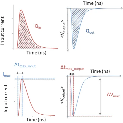
The key point is how the output parameters of the VCO chain can give information about the input current. This could be done through the analysis of various characteristics extracted from the average voltage variation (Fig. 3). The first
parameter is the variation of the average output signal (ΔVmax)
versus the maximum of the input current (Imax) for different
particle charges (Fig. 4). As shown in [10], the linearity of Fig. 4 is exactly the same for the different deposited charges. In [12], it has been demonstrated that two different currents with
the same maximum value have the same corresponding ΔVmax.
ThenΔVmax does not depend on the shape of the current but
only on the current peak. Thus the measurement of ΔVmax
appeared to be a reliable parameter to recognize the current peak of the input signal. The second parameter is the variation
of Δtmax (Fig. 3). For the input, Δtmax_input is the difference
between the time corresponding to the maximum of the current and the beginning of the current variation. For the
average voltage at the output, Δtmax_output is the difference
between the time corresponding to the minimum of the voltage and the beginning of the voltage variation. These two times correspond to peaking times. They are not considered in the paper. The last curve (Fig. 5) is the integral (area of the signal
drop) of the average output signal Qout versus Qin(Fig. 3). This
curve allows the charge identification through this detection system. Through these curves, the output parameters can be
linked to the input currents, what could allow the incoming particle identification.
To get reliable results, the resolution of the system has to be checked. The degradation of the system response is clearly visible in Fig. 4 and 5. The results are good if the points are included in the “good detection” zone. This zone corresponds to a linear response of the system in the range ±10 %. When results are out of this zone, the resolution is clearly degraded [13] and the pulse characteristics are also not suitable with the resolution of our system.
Fig. 4. Variation of the average output signal (ΔVmax) versus the maximum of
the input current (Imax).
Fig. 3. Definition of the characteristics of the input and output signal .
4
Fig. 5. The integral (area of the signal drop) of the average output signal Qout
versus Qin.
V. CASE-STUDY: ALPHA PARTICLE CROSSING A 3X3 DETECTION CELL
A. The 3x3 detection cell
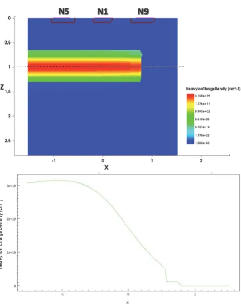
Fig. 6. 3x3 matrix including the name of the contact zones.
In order to improve the efficiency of the detection and the tracking ability, a 3x3 matrix is modeled and analyzed (Fig.6). The input current is no longer the simplified current given in equation (1). Now the current source comes from the realistic simulation of the matrix using TCAD device simulation tools (Synopsis ©) (Fig. 10). The effect of the ion strike is
simulated using the Heavy Ion module of Synopsis [14],
considering an electron-hole pair column centered on the ion track axis. The Linear Energy Transfer (LET) is defined as the energy lost by the particle, by unit of length. It varies along the track. In TCAD studies, a constant LET is sometimes used for simplification purposes. However, if the approximation of a constant LET is reasonable, it is not realistic. Indeed, this parameter varies along the track and is linked to the initial
energy of the particle [15]. Thus a real variation of the LET
was integrated in our simulations based on the value given by
SRIM tables [16]. As this detector is suitable for low energy
particles detection, the simulated ion is an alpha particle crossing the device with an initial energy of 0.6MeV which
corresponds to a range of 2.3μm. The generation of such a
particle in the whole structure is shown in Fig. 7 (2D heavy
ion charge density and 1D variation of the heavy ion charge
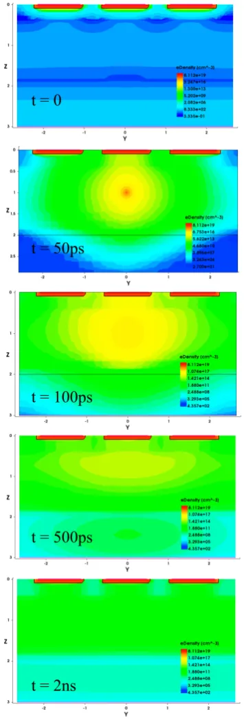
density). The evolution of the charge density is shown in Fig.
8 and Fig. 9 for the two cut-planes presented in Fig. 6. The particle is generated at 50ps. The current generated by the particle crossing are shown in Fig. 10 at each electrode.
B. Alpha particle tracking using the VCO
The nine currents generated using Synopis were injected in the nine VCOs in order to test the suitability of the studied VCO to our detection cell. Unfortunately, the resolution of our system was not good enough to allow a good the detection of the currents generated by the detection cell. This was expected because the duration of the signal is near 0.4ns, what corresponds to an input signal frequency of 2.5GHz, too fast to be detected by a 2GHz oscillator. Thus, even if an average voltage is obtained for the zone labeled N5 (Fig. 11), the
Imax-ΔVmax couple is clearly out of the detection zone (Fig.
12) what means that the other lower currents are also out of this zone. Moreover, except for the N1 and N5 average voltages, the others are in the noise limit. So we cannot be confident about the obtained curves of Fig. 11. Then we tested the same currents with another VCO developed with a higher frequency (4.3GHz). The detection is better (Fig. 13). However, we cannot conclude about the resolution without the linearity curve.
Fig. 7. 2D heavy ion charge density and 1D variation of the heavy ion charge density.
Fig. 8. Evolution of electron density in the Y direction.
Fig. 9. Evolution of electron density in the X direction.
Fig. 10. Currents from the pixels
-1,0E-05 1,0E-05 3,0E-05 5,0E-05 7,0E-05 9,0E-05
0,0E+00 2,0E-10 4,0E-10 6,0E-10 8,0E-10 1,0E-09
Cu
rre
nt
(A
)
Time (s)
Zone N1 Zone N2 Zone N3 Zone N4 Zone N5 Zone N6 Zone N7 Zone N8 Zone N9
t = 0
t = 50ps
t = 100ps
t = 500ps
t = 2ns
t = 0
t = 50ps
t = 100ps
t = 500ps
Fig. 11. Average voltages corresponding to the currents of Fig. 10.
Fig. 12. Variation of the average output signal (ΔVmax) versus the maximum of the input current (Imax) including zone N5.
Fig. 13. Average voltages corresponding to the currents of Fig. 10 with a VCO developed with a higher frequency (4.3GHz).
VI. CONCLUSION
The detection chain presented in this work is based on an innovative concept based on an indirect detection through a voltage controlled oscillator. The analysis of the results extracted from this chain showed the possibility to recognize the input signal by using the average voltage of the output signal. The main advantage of this system is the possibility to get all the information related to the input signal (shape and order of magnitude of the current and duration) with a good sensitivity of detection.
Here we have explored the detection limit of the presented VCO. For the pixel matrix simulated in this paper, a higher frequency has to be used. Indeed, increasing the time resolution of the detected pulse is required and the system resolution could be tuned by changing the oscillation frequency. Calibrating the oscillator frequency is also a solution for spectrometry analysis. In that case, several VCO working at different frequency could be used, giving the opportunity to characterize accurately a given environment.
REFERENCES
[1] Ying Zhang, Christine Hu-Guo, Daniel Husson, The-Duc Le , Stéphane Higueret, Yann Hu, “A High-Sensitivity Low-Power CMOS Sensor for a Future Neutron Personal Dosimeter”, in IEEE Trans. On Nucl. Sc., vol.59, no.4, pp. 1465-1471, August 2012.
[2] Xilinx, Customer Advisory: Flip-Chip Package Substrate Solder Issue, January 19, 2004.
[3] J.F. Ziegler, H. Puchner, “SER – History, Trends and Challenges: A Guide for Designing with Memory ICs”, pp. 3-18, 2004.
[4] L.W. Massengill, “Cosmic and Terrestrial Single-Event Radiation Effects in dynamic Random Access Memories”, in IEEE Trans. On Nucl. Sc., vol.43, no.2, pp. 576-593, April 1996.
[5] Trigano, A; Hubert, G; Marfaing, J; Castellani-Coulié, K ”Experimental study of neutron-induced soft errors in modern cardiac pacemakers”, Journal of Interventional Cardiac Electrophysiology (JICE), 2010 [6] Bradley, P., & Normand, E. (1998). implantable cardioverter
defibrillators. Institute of Electrical and Electronics Engineers. IEEE Transactions on Nuclear Science, 45 (6), 2929–2940.
[7] Physician Advisory from Saint Jude Medical, Inc, October 6, 2005. Kohanyi, G. and Fain, E.
[8] Saint Jude Medical advisories. Available at: http://www.hc-sc.gc. ca/dhp-mps/medeff/advisories-avis/prof/2005. Accessed 14 April 2011.
[9] Ferrick, A., Bernstein, N., Aizer, A., & Chinitz, L. (2008). Cosmic radiation induced software electrical resets in ICDs during air travel. Heart Rhythm, 5(8), 1201–1203.
[10] K. Castellani-Coulié, H. Aziza, W. Rahajandraibe, G. Micolau, J.-M. Portal, "Development of a CMOS Oscillator Concept for Particle Detection and Tracking", IEEE Trans Nucl. Sci., 2013.
[11] K. Coulié-Castellani, W. Rahajandraibe, G. Micolau, H. Aziza, J.-M. Portal, "Improvement of a detection chain based on a VCO concept for microelectronic reliability under natural radiative environment", IEEE LATW Conference, 2015.
[12] S. Ben Krit, K. Coulié-Castellani, W. Rahajandraibe, L. Ottaviani, G. Micolau, H. Aziza, J.-M. Portal, “Comparison of a Readout Chain Dedicated to the Signal Conditioning of a Particle Detector and an Innovative Chain Based on a VCO Concept”, RADECS 2015, Moscou, Russia, September 2015.
[13] Castellani-Coulié K., Aziza H., Micolau G. and Portal J-M., “Optimization of SEU Simulations for SRAM Cells Reliability under Radiation”, Journal of Electronic Testing, February 2012
[14] TCAD Sentaurus user’s manual (Synopsys).
1,25 1,2505 1,251 1,2515 1,252 1,2525 1,253 1,2535
4,0E-09 5,0E-09 6,0E-09 7,0E-09 8,0E-09 9,0E-09
<Vout
put
>
Time (s)
1,28 1,285 1,29 1,295 1,3
3,0E-09 4,0E-09 5,0E-09 6,0E-09 7,0E-09 8,0E-09
<Vout
put
>
Time (s)