Publicat de
Universitatea Tehnică „Gheorghe Asachi” din Iaşi Tomul LIV (LVIII), Fasc. 3-4, 2008
Secţia
AUTOMATICĂşi CALCULATOARE
DATA STORAGE METHOD FOR SYSTEMS WITH 8 BIT
MICROPROCESSORS OR MICROCONTROLLERS
BY
ALEODOR DANIEL IOAN
Abstract. This paper presents a method of data storage for micro-systems based on 8-bit microprocessors or microcontrollers that have external buses available, by using an original interface for connecting standard hard disk and CD-ROM drives. Because such devices have 16-bit wide data bus, a special interface is required to split the 16-bit IDE/ATA data transfer in two consecutive 8-bit bus transactions. The interface can be made by software using I/O ports, but in this case all commands and signal strobes to the IDE/ATA device must be implemented by programming, thus slowing down the data transfer rate and increasing the software complexity. A hardware interface can take benefit of the already existent /RD & /WR bus strobes which are wasted by software approach and the block I/O instructions that some microprocessors have. The interface proposed here is a tuned compromise between hardware complexity and efficient use of block I/O instruction: the speed is maximized for read and is less for write, because reads are more frequent than writes. A block schematic is presented, together with a prototype implementation used for testing.
Key words: hard disk drives, embedded systems, bus transactions, hardware
strobes, block I/O instructions, sector read/write subroutines, prototype implementation. 2000 Mathematics Subject Classification: 62K10, 68M99.
1. Introduction
The IDE/ATA interface is widely used in personal computers to connect hard disk drives, CD-ROM drives and DVD drives [1]. The IDE/ATA controller of modern personal computers is a specific integrated circuit known as a “super I/O chip” or it is integrated in the chipset bridge of the motherboard that adapts memory and peripheral buses to main processor bus. This controller uses 16-bit wide data bus that matches the width of the IDE/ATA data ports [1] and can be interfaced directly with the devices.
Because the capacity of hard disk drives has been increased exponentially in the last years and smaller capacity drives have become
cheaper, a new use of these devices has been emerged: connecting hard
disk drives to some embedded systems used in automatic control
applications [2].
If the microprocessor or the microcontroller used in that embedded system has 16-bit wide data bus, the connection can be made directly and no interface is required. But if the CPU has 8-bit data bus, things become more complicated, and a special interface is required to split the 16-bit data transfer in two consecutive 8-bit bus transactions [3].
To simplify this interface, some micro-systems use a software emulation of the interface on the parallel ports contained within or added to the microcontroller [2]. This kind of approach reduces the performance significantly, because it is difficult for the software to handle both negative and positive changes in all signals (chip selects and read/write strobes) in a coherent sequence, together with the read/write of the port used for data transfer. Therefore, the transfer speed is reduced to instruction execution level and the software overhead is significant.
Especially if the micro-system uses a microprocessor or the microcontroller used has external buses available [4], a hardware approach should be considered instead, because it simplifies the software and increases the speed by using hardware read/write strobes and in some cases even the input/output block instructions, which some microprocessors may have [5].
In this paper I propose an original variant of a hardware interface that is optimal because it can take benefit of both hardware strobes and block instructions, it is universal enough to be used in conjunction with many microprocessor or microcontroller based embedded systems, it uses no special programmable devices (like PAL or GAL [6]) and it can be implemented with discrete logic or within a FPGA or CPLD device.
2. IDE Peripheral Device
According to the “AT Attachment Interface” standard [7], a hard disk or CD-ROM drive is an intelligent device that contains all the circuitry needed to control the drive mechanism that implements the physical interface for the magnetic or optic storage disk [1]. The IDE stands for “Integrated Drive Electronics”.
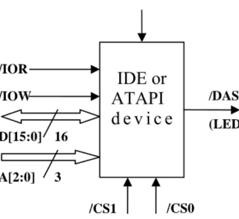
From the user’s point of view, the IDE device can be reduced to a digital programmable peripheral interface, not much different from the classical microprocessor peripheral family of circuits [3]. After doing some research [1], I concluded that an IDE device has an 16-bit wide data bus, with slave /RD & /WR read and write strobes, 3 address bits for register selection, 2 active low chip selects, an activity LED drive signal and an active high RESET signal,
together with some other auxiliary signals that will not be used in this application, like in Fig. 1.
The /CS0 signal selects the command block registers, in conjunction with the appropriate address placed on the A[2:0] bits. These registers should be seen by the central processing unit as 8 I/O ports and they are enough for the most functions of the drive.
The /CS1 signal selects the control block registers, but with only 2 addresses (6 and 7) placed on the address bus A[2:0]. The rest of addresses are unused and remain in high impedance state when reading. These 2 I/O ports are used for auxiliary functions of the drive and they can be ignored in most common cases. When neither /CS0 or /CS1 is active, the device remains idle, in high impedance state. Of course, the two chip select signals cannot be both active at the same moment [1].
Fig. 1 – IDE main connections.
The registers addressed by both chip select signals are 8-bit wide and their reading or writing is made by using the lower byte D[7:0] of the 16-bit data bus. Only the data port with address [A2A1A0]=0, used for data transfers, is 16-bit wide. Table 1 shows the function of each command block register, selected with /CS0 as 8 command output ports when writing or 8 input status ports when reading [7].
The main problem when connecting such an IDE/ATA device to 8-bit micro-systems is that the data port must be accessed in two distinct sequences of 8-bit each [3]. Accessing the other ports does not require double sequenced bus transactions. Because the 8-bit microprocessor or microcontroller can read only 8-bits at the same time, one of the two bytes provided by the IDE device on the 16-bit wide data bus when reading must be saved into an external latch when the other is sent to the microprocessor.
IDE or
ATAPI
d e v i c e
/DASP (LED) /IOR /CS1 /IOW /CS0 RESET D[15:0] 16 A[2:0] 3Table 1
Registers Addressed with /CS0
A2A1A0
(BIN (/IOR) Read (/IOW) write (BITS) width
0 0 0 Data Port Data Port 16
0 0 1 Error Features 8
0 1 0 Sector Count Sector Count 8 0 1 1 Sector Number
(LBA 0-7) Sector Number (LBA 0-7) 8 1 0 0 Cylinder Low
(LBA 8-15) Cylinder Low (LBA 8-15) 8 1 0 1 Cylinder High
(LBA 16-23) Cylinder High (LBA 16-23) 8 1 1 0 Drive/Head
(LBA 24:27) Drive/Head (LBA 24-27) 8
1 1 1 Status Command 8
3. Interfacing to 8-Bit Wide Data Bus
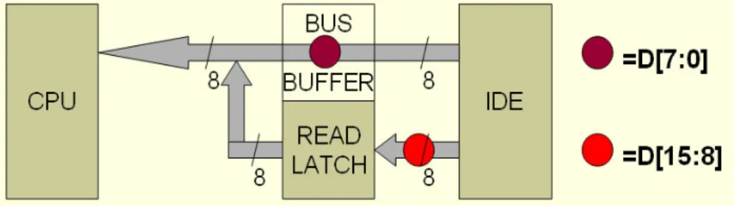
The latch must be locked at the same moment with the deactivation of the /IOR read signal, when the CPU sampled the data bus internally. The next bus transaction must be a read of the output of this external latch onto the CPU 8-bit wide bus.
The simplest configuration is to send the lower byte (from D[7:0]) directly to the microprocessor through a transparent bus buffer, and to latch the high byte (from D[15:8]) to be read in the next cycle (Fig. 2). In this way data bytes are read in the usual order, first the low byte and next the high byte.
Fig. 2 – The principle for data reading.
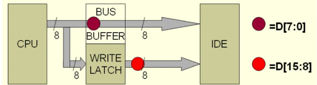
At writing, because the device samples all the 16 data bits at deactivation of the /IOW write signal, the write cycle requires that both high and low byte be available at the very same moment. To satisfy this condition, one byte must be saved into an additional external data latch by the previous bus
transaction, and both, the data latch output and the other byte from the CPU must be sent to the IDE 16-bit data bus at the next bus transaction.
To respect the previous rule, with the low byte first and the high byte next, the low byte should be saved into the external latch and the high byte should be taken directly from the microprocessor data bus. This configuration keeps the order of bytes, but it is not optimal for hardware implementation, because the CPU data bus should be connected to the low IDE data bus at reading and to the high IDE data bus when writing. This implementation would require two additional bus buffer circuits, for multiplexing the CPU three state data bus.
For minimal hardware implementation, I chose to connect the CPU bus directly to the lower D[7:0] IDE bits, using only one bidirectional bus driver that is required to adapt and to separate the IDE cable (susceptible to the noisy environment [1]) from the micro-system bus. Of course, the two latches for read/write must be used further in this kind of implementation.
Fig. 3 – The principle for data writing.
So, at writing, the microprocessor or microcontroller should first write the high byte to the external write latch. Then, at the next write cycle, both the latch output (placed on D[15:8]) and the low byte from CPU (placed on D[7:0]) will be sent to the IDE/ATAPI device (Fig. 3). The low byte will be sent through the same transparent bus buffer used at reading, which should be bidirectional.
However, this solution has some drawbacks, because the order of bytes must be inversed at writing. This can lead to the impossibility to use the block output instructions that some embedded microprocessors have. But, because the interface cost depends mainly on hardware and because the writes to a hard disk drive device can occur with only about 25% probability [6] and the reading can still use the block input instructions, I consider this a quite optimal idea.
4. Functional Description
Considering those presented above, I propose a block diagram for the interface (Fig. 4), as an outcome of my research an practical experiments.
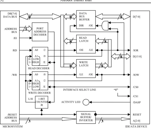
Fig. 4 – Block diagram of the IDE/ATA interface.
The low IDE data bytes D[7:0] will pass through the bidirectional data bus buffer with three state outputs, buffer which is enabled at both reads and writes by the AND gate with OR function for active low signals [6]. The direction of the buffer is from the IDE to the micro-system when reading and reversed when writing.
The high IDE bytes are locked into the read latch when reading the low bytes and are taken from the write latch when writing the low bytes. Both read and write latches should have three state outputs [6].
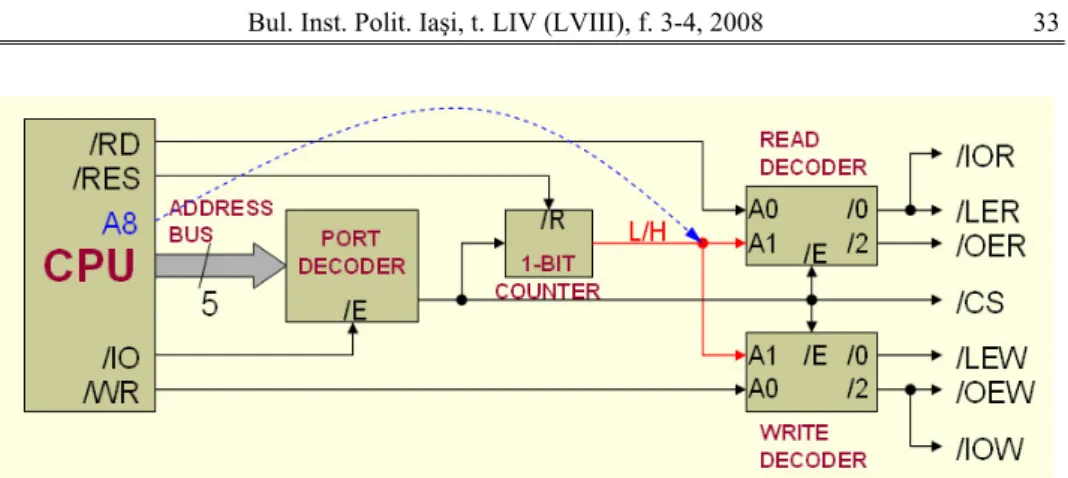
The control of the latches and /IOR & /IOW signals is derived from the /RD & /WR lines of the microprocessor by two distinctive 2:4 decoders, used here as demultiplexers [6], like in Fig. 5. The A1 line of both decoders is used to switch the data transfer between the IDE and the high byte latches. A 1-bit counter (with one flip-flop) toggles this line at each consecutive interface transfer.
The read decoder generate /IOR signal for IDE and read latch enable (/LER) when L/H=0, then output enable for read latch (/OER) when L/H=1. The write decoder generate write latch enable (/LEW) when L/H=0, then output enable for write latch (/OEW) and /IOW signal for IDE when L/H=1.
8 8 8 8 8 8 8 8 DATA BUS BUFFER DIR /OE READ LATCH /OE /LE WRITE LATCH /LE /OE PORT ADDRESS DECODER 5 SIGNAL BUFFER/ INVERTER 1-BIT COUNTER /R DB[7:0] DATA BUS /RD /WR ADDRESS BUS /IO /RESET ADDRESS BUS 3 3 /IOR D[15:8] D[7:0] /IO /0 /2 A0 A1 /E READ DECODER ACTIVITY LED /2 /0 A0 A1 /E WRITE DECODER L/H W /CS0 A[2:0] RESET /DASP /CS1 “1”
INTERFACE SELECT LINE
MICROSYSTEM IDE/ATA DEVICE
0= LOW 1= HIGH
0= HIGH 1= LOW
Fig. 5 – Control signals generation.
First reading of the data port will activate the low byte buffer and store the high byte into the read latch and the next reading will activate this read latch, and so on, because each reading will toggle the L/H line.
At writing, things are reversed: first writing will store the high byte into the write latch and the next writing will activate both the low byte buffer and the output of this write latch. This is the reason for reversing the connection from the /0 & /2 outputs of the write decoder.
Because the L/H counter is cleared only once at system reset, care should be taken when accessing the other non-data 8-bit ports from the IDE device: each read/write cycle should be doubled to restore the initial state of the counter. At reading, the first read is valid and at writing, the second write is valid.
A 6-bit decoder provides the active low interface select signal, which is used to enable the read/write decoders, to activate the IDE chip select signal /CS0 and to increment the L/H counter.
Assuming that most of the 8-bit micro-systems have an 8-bit I/O address space [5], the port decoder needs to handle 5 address bits and one /IO request line for peripheral access. This should still be true with some memory mapped I/O that some microcontrollers have [4], when a memory read/write signal is used instead. The /CS1 signal for IDE device is not used here and therefore is permanently disabled.
For separation between the IDE cable and the micro-system bus, each signal that is coming from one to another must be buffered and cannot be directly connected [6]. Because most micro-systems have an active low reset signal [5] and the IDE has an active high RESET [7], it is more convenient to have a buffer with inverted outputs that invert the three address bits used for IDE register selection, too. This, of course, will lead to a reversed order of ports that can be handled in software.
Finally, a LED can be connected at /DASP signal to indicate device activity [1].
5. Using Special I/O Block Instructions
Some microprocessors used in embedded systems have instructions for block transfer between memory and I/O ports [5]. The use of such instructions can simplify the interface design and can also boost the transfer speed.
For example, the interface can be optimized when used in conjunction with Hitachi HD64180 microprocessor or with Zilog Z84C15 intelligent peripheral controller. They are both modern upgrades that include the CPU and all the peripheral circuits from old Z80 microprocessor family [8].
Such embedded microprocessors have block I/O instructions that can transfer an entire data block between memory and an I/O port. The INIR/INDR & OTIR/OTDR (“Input/Output, Increment/Decrement and Repeat”) instructions [5] can transfer a data block between memory address (HL) and the I/O port address (C), with length in register B (maximum 256 bytes). The address counter HL is incremented/decremented and the length counter B is decremented after each cycle, until B=0. The byte counter is also placed on the upper 8-bit address bus at I/O access.
This facility gave me the idea to use the address bit A8 as the low/high byte select, removing the L/H 1-bit counter from the interface schematic (the A1 line of both read/write decoders will be connected directly to A8, see bypass arrow in Fig. 5). This line will be driven by bit zero of the register B and will toggle at each transferred byte, because the counter is decremented: even-odd-even-odd…
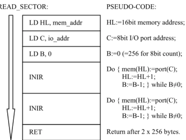
If the block length counter B is initialized with 0, then 256 bytes will be transferred from the interface with one INIR instruction in a fast burst. It is interesting to suggest that with only two INIR instructions, an entire sector of 512 bytes can be read from the IDE/ATA device, like in the subroutine designed by me which is shown in Fig. 6.
READ_SECTOR: PSEUDO-CODE:
Fig. 6 – Sector reading algorithm.
HL:=16bit memory address; C:=8bit I/O port address; B:=0 (=256 for 8bit count); Do { mem(HL):=port(C); HL:=HL+1; B:=B-1; } while B≠0; Do { mem(HL):=port(C); HL:=HL+1; B:=B-1; } while B≠0; Return after 2 x 256 bytes. INIR INIR LD B, 0 LD HL, mem_addr LD C, io_addr RET
This simple subroutine gives more than 500 Kbytes per second transfer speed with only 16MHz processor [8] when tested, more than enough for any automatic control applications.
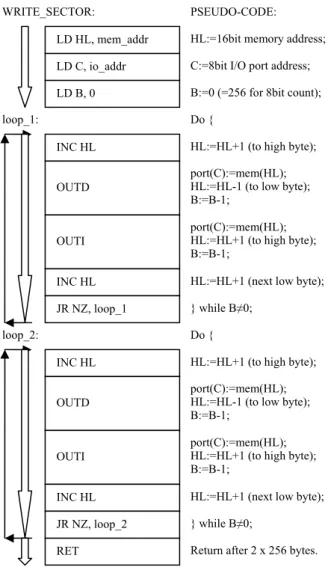
Unfortunately, the same solution cannot be used at writes, due to the reversed order of bytes that this interface requires. The CPU should send first high-then-low byte to the interface, but in memory bytes are always stored in the reversed low-then-high order. A more complex approach is needed, by moving the memory pointer between consecutive writes up to high byte, down to low byte and then up with two positions to the next high byte, and so on…
The next subroutine, also personally designed (Fig. 7), writes an entire sector of 512 bytes to the IDE/ATA device, using the OUTI/OUTD instructions that work in the same way like OTIR/OTDR, but with no automatic repeat [5].
Fig. 7 – Sector writing algorithm.
WRITE_SECTOR: PSEUDO-CODE: loop_1: loop_2: LD B, 0 LD C, io_addr LD HL, mem_addr INC HL OUTD OUTI INC HL JR NZ, loop_1 RET INC HL OUTD OUTI INC HL JR NZ, loop_2
HL:=16bit memory address; C:=8bit I/O port address; B:=0 (=256 for 8bit count);
Return after 2 x 256 bytes. HL:=HL+1 (to high byte); port(C):=mem(HL); HL:=HL-1 (to low byte); B:=B-1;
port(C):=mem(HL); HL:=HL+1 (to high byte); B:=B-1;
HL:=HL+1 (next low byte); } while B≠0;
Do {
HL:=HL+1 (to high byte); port(C):=mem(HL); HL:=HL-1 (to low byte); B:=B-1;
port(C):=mem(HL); HL:=HL+1 (to high byte); B:=B-1;
HL:=HL+1 (next low byte); } while B≠0;
The write speed is still higher than a code without the use of block instructions, and overall performance is maintained, because in most cases the micro-system needs to read the disk.
It should be noted, as it results from the above examples, how powerful such instructions are, when more or complex pseudo-code statements can be programmed by only one instruction in the assembly language. It is obvious that any implementation of this algorithm in high level languages is out of discussion, because it will be compiled into more instructions of the microprocessor, significantly reducing the speed and the efficient use of the interface hardware.
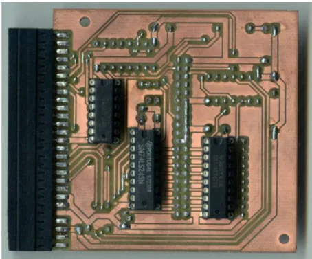
6. A Prototype Implementation
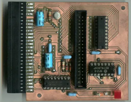
To test this hardware interface, I have designed a detailed schematic with discrete logic integrated circuits, based on the block diagram that was presented above. For this practical schematic, I have designed a layout in “Protel 99SE” and then I have made a printed circuit board by using the “Protomat C60” prototyping machine (Fig. 8). The prototype board was useful also for the design of sector transfer subroutines.
Fig. 8 – Top side of the prototype board.
In the electronic schematic, one inverter circuit, a transistor, some more resistors and a few decoupling capacitors were necessary, for the following
reasons: the LE signal of real latches is active high and must be inverted, the AND gate controlling the /OE signal of the bus buffer was implemented by two diodes and a resistor to minimize package count and a transistor was used for buffering the /RESET signal.
It is well known that one decoupling capacitor is required per each package of integrated circuit. It should be noted also that all the 6 inverters from the corresponding package were useful, 2 for inverting the LE signals, 3 for inverted buffering of the address lines to IDE device, and 1 for delaying the /IOR signal to appear after activation of LE for the read latch. Delaying of the /IOW signal is not required, because it was connected straight to /OE of the write latch.
The layout is quite optimal, because the circuits are placed on both top-and-bottom layers to minimize board surface and routing complexity (Fig. 9).
Fig. 9 – Bottom side of my prototype board.
One interesting solution that I found was to intercalate the pin rows of read and write latches, by placing one on top and the other on bottom. The entire routing process was done manually because this is the only way to design a good printed circuit board (the ground structure should be carefully routed in correspondence with the position of the decoupling capacitors, to minimize noise and parasite coupling by power lines, the tracks must be routed with obtuse corners to eliminate reflections, etc.).
7. Conclusions
The interface described here can be useful for any micro-system with microprocessor or microcontroller that has external bus connections and requires large and fast data storage. With software file system support, the micro-system can access a large amount of data from hard disk drives or CD-ROM drives created by various computer operating systems.
This implementation in hardware is much more efficient and gives about 100 times the speed obtained from software implementation with step-by-step control over the data & address bus and the /RD & /WR strobes by port lines [2]. Use of the already available hardware strobes is the obvious solution and enables the functionality of block transfer instructions that simplify the software and reach the maximum transfer speed obtainable with an 8-bit micro-system.
The interface can be implemented into a programmable device such as the CPLD or FPGA chips to minimize the external logic and the PCB routing requirement.
Received: September 16, 2008 “Gheorghe Asachi” Technical University of Iaşi, Department of Automatic Control and Applied Informatics
e-mail: [email protected]
R E F E R E N C E S
1. Schmidt F . , The SCSI Bus and IDE Interface: Protocols, Applications &
Programming. 2nd Ed., Addison-Wesley, New York, 1999.
2. Stoffregen P. , Using an IDE Hard Drive with a 8051 Board and 82C55 Chip. unpublished, http://www.pjrc.com/tech/8051/ide, 1999.
3. Ball S.R., Embedded Microprocessor Systems: Real World Design. 2nd Ed.,
Butterworth-Heinemann, Woburn, 2000.
4. Mazidi M . A . , Mazidi J . G . ,The 8051 Microcontroller and Embedded Systems. Prentice Hall, New Jersey,2000.
5. Gaonkar R. M., Z-80 Microprocessor: Architecture, Interfacing, Programming, and
Design. 3rd Ed., Prentice Hall, New Jersey,2000
.
6. Mano M.M., Kime C.R., Logic and Computer Design Fundamentals. 3rd Ed., Prentice
Hall, New Jersey,2004.
7. ***AT Attachment Interface. Technical committee for the international committee on
information technology standards (INCITS X3.298-1997), http://www.t13.org, 1997.
8. *** Z84C13/Z84C15 Enhanced Intelligent Peripheral Controller Product
METODĂ DE STOCARE A DATELOR PENTRU SISTEME CU
MICROPROCESOARE SAU MICROCONTROLERE PE 8 BIŢI
(Rezumat)
Se prezintă o metodă de stocare a datelor pentru micro-sistemele bazate pe microprocesoare sau microcontrollere de 8 biţi care au magistralele disponibile extern, prin utilizarea unei interfeţe originale de conectare a hard disk-urilor şi CD-ROM-urilor standard. Din cauză că astfel de dispozitive au magistrala de date cu lăţimea de 16 biţi, o interfaţă specială este necesară pentru a împărţi transferul de date IDE/ATA pe 16 biţi în două tranzacţii consecutive pe magistrala de 8 biţi. Interfaţa poate fi realizată prin soft folosind porturile de intrare/ieşire, dar în acest caz toate comenzile şi semnalele de control al transferului pe magistrală trebuie implementate prin programare, reducând în acest fel rata de transfer a datelor şi mărind complexitatea softului. O interfaţă hard poate beneficia de semnalele deja existente /RD şi /WR pentru controlul transferului care sunt irosite prin abordarea soft şi de instrucţiunile de intrare/ieşire pentru blocuri de date pe care unele microprocesoare le au. Interfaţa propusă este o soluţie de compromis între complexitatea hard şi utilizarea eficientă a instrucţiunilor de intrare/ieşire pe bloc: viteza este maximă la citire şi este puţin mai redusă la scriere, deoarece citirile sunt mai frecvente decât scrierile. Este propusă o schemă bloc, împreună cu o implementare prototip utilizată la testare.