Published By:
Abstract—This paper presents the careful study of sigma-delta analog to digital convertor. The operations, characterizing parameters and totally different structures projected square measure conferred in basic type. the varied techniques and strategies for the design of a CMOS 3rd order Continuous Time (CT) Sigma Delta (SD) Modulator, where in to enhance the gain of the loop filter and to avoid the loading effect of the succeeding stage, facile differential pairs square measure enclosed between the passive RC integrators. then the ADC are optimized victimization Genetic Algorithms so as to realize the nice exchange between RC variations and loop stability.This makes SD-ADC more advantageous compared to conventional converters, that makes possible to use this SD-ADC in bio-medical applications.
Index Terms— Sigma-delta ADC, passive RC integrators, optimization techniques, bio-medical applications, differential pairs.
I. INTRODUCTION
Data conversion is an important element in any electronic system and as all the real time natural signals are analog in nature we need to 1nalog to digital conversion using Sigma Delta ADC is a price effective and high resolution method. The Sigma Delta modulator was initial introduced in around 1962, and it came into usage recently after the evolvement of digital VLSI technology
The main benefits of Sigma Delta ADC are: High reliability
Increased functionality Reduced chip cost
A delta-sigma ADC 1st encodes associate analog signal exploiting high-frequency delta-sigma modulation, and subsequently applied to a digital filter to create a higher-resolution, lower sample-frequency digital output. Primarily owing to its low value potency and reduced circuit complexness, utilization of this method is enhanced in latest electronic systems like DACs, ADCs, frequency synthesizers, switched-mode power supplies and motor controllers. The quantal output of a delta-sigma modulator is sometimes used directly in signal process.
Sigma delta modulators have been briskly scrutinized for low voltage biomedical applications. Many electronicmedical devices are portable in which battery life is limited. Therefore design of sigma delta ADCs with
Revised Version Manuscript Received on July 18, 2019.
B. Hemalatha, Research Scholar,Amity University, India. (email: [email protected])
Dr. Ajay Kumar Dadoria, Asst.Professor, Amity University, India. (email: [email protected])
Dr.Harishankar Srivastava, Assoc.Professor, Anurag Group of Institutions,Hyderabad, Telangana, India. (email: [email protected])
reasonable performance became very popular in medical applications.
The classical access for the implementation of a continuous time (CT) SD Modulator needs a number of amplifiers identical to the order of the loop filter [1]. Any how, for the last few years several design strategies and techniques were advanced using which many SD-ADCs have been designed and implemented with the number of amplifiers less than the order of the loop filter.[2-5] and CT SD-ADC were also designed without a single amplifier [6-8] In [5], a higher order i.e. 5th order CT hybrid active-passive SD modulator is designed, but this implementation could not achieve greater than 10-bit effective resolution. In [3], a 3rd order loop filter using a single amplifier was designed ,it can achieve 11-bit resolution. This design provides a good compromise between area and energy. In [6], a passive CT-SD converter is designed without using amplifiers ,built with only 2 passive integrators and 1-bit comparator. But the dynamic performance using this method, cannot reach more than 8.5 bit effective resolution.
Researchers have designed various configurations of sigma delta ADCs. Conventional SD-ADCs were designed with operational amplifier topology, where the number of amplifiers is equal to the order of loop filter. Later SD-ADCs were designed with the number of amplifiers less than the order of the loop filter,which provided a good compromise between area and energy efficiency. Then after amplifier less SD-ADCs were designed,where in all the amplifiers in the loop filter were removed, to provide high energy efficiency. Conventional SD Modulators are designed with an active integrator circuits are employed in the loop filter. Later these active integrators in the loop filter circuit are replaced by a passive integrator circuits, so as to reduce power dissipation and also it is easy to design due to less stability design concerns. In a passive integrator circuit there is no need to design a high gain amplifier. The difference between the active and passive integrator circuits will be only the DC gain.
Hybrid structure of SD-ADCs were also designed, in which both active and passive integrators are used. Active integrators with amplifiers provide high gain and passive integrators helps in saving the power.
The proposed sigma delta modulator will be designed using passive RC integrators and also differential pairs are inserted between the integrator stages to avoid the loading
Techniques for Sigma Delta ADC Design using
CMOS Technology for CODEC
effect of the succeeding stage and also to provide enhanced gain for the integrator or loop filter. Sigma delta ADC with passive integrator design will increase the energy efficiency and requires low power and low chip area.
II. COMPARISION OF ACTIVE AND PASSIVE SD MODULATORS
[image:2.595.311.552.50.216.2]According to [6] and [9], Hybrid SD modulators have become highly regarded owing to their high energy potency. the main concept of this hybrid structure is to switch the active integrators with the passive integrators within theloop filter of SD ADC. This curtails the power dissipation and it it easy to style as there are less stability problems in passive integrators as a result of it's now not required to design the complex high gain amplifiers.
Fig. 1. RC integrators: (a) Passive and (b) Active.
[image:2.595.54.290.255.333.2]The only difference between the active and passive RC integrators is its DC gain. However, the major drawback of using all passive integrators circuits at very low sampling frequencies, requires higher RC time constant and hence more area. Therefore the proposed CT passive converter is not much suitable for signal bandwidth in 10s or 100s of kHz range. For greater bandwidths around 100s of kHz to MHz, the time constant required may be comparably small. When compared to active integrator circuit, the proposed passive RC integrator at high frequencies requires less area. The signal gain of passive integrator is A times greater than the active integrator and output spectra of both the passive and active integrators will be the same.
Fig. 2. Block Diagram of Single bit SD Modulator
[image:2.595.313.561.256.410.2]A passive circuit enhances the gain of the SD modulator through the comparator, rather than using an amplifier circuit. The advantages of this passive circuit design are it is easy to design, less power dissipation and it operates at lower operating voltages. The disadvantage with this passive circuit is very small input signal (thermal noise) to the comparator shows a serious result on the signal to noise ratio of the SD modulator.
Fig. 3. Loop filter’s output voltages of a 1st order SD Modulator
Fig. 4. Comparator gain versus input signal amplitude
for a 1st order SD Modulator
III. ORDER -2 CT SD MODULATOR WITHOUT AMPLIFIER
So as to enhance the SNDR of SD Modulator it is required to decrease the quantization noise and thermal noise within the signal band. The quantization noise can be shriveled by enhancing the loop gain within the signal band. But this results in either a smaller BW or larger sampling frequency. The ratio of in-band gain and the gain at sampling frequency can be enhanced by increasing the order of the filter with the addition of integrators to the loop. It is necessary to either increase the feedback paths or to feature zeros into the loop filter to form the closed loop system stable.
D out(s)
H1(s) H2(s)
DAC
C
fs
Vin (s)
b
k
[image:2.595.56.289.531.626.2] [image:2.595.322.542.619.708.2]Published By: In a passive SD modulator, the only gain is that obtained at
the comparator i.e, there is no use in adding second feedback path as the gain divides ino two loops and hence no extra reduction in the quantization noise can be achieved. With only one feed back path , we can have a stable closed loop system, by adding a zero to the loop filter, this gives a hgh loop gain which is provided by the comparator.
Fig. 6. Electrical schematic of the 2nd order CT SD Modulator
Cascaded connection of 2 RC circuits can be used to obtain a 2nd order noise shaping. This loop filter has 2 poles that are very close to zero so as enhance the reduction of the quantization noise. A zero must be introduced in the circuit to manage the oscillating performance of the system with two open loop poles that are close together. Zero can be introduced by connecting an extra resistor in series with a capacitor in the second section of RC circuit as shown in fig 9.
Fig. 7. Output spectra of a 2nd order SD Modulator
[image:3.595.312.547.48.275.2]The output spectra of a 2nd order CT SD modulator with an ideal comparator (when the comparator noise is not considered) and the loop filter contrived with a either active or passive approach would be similar.
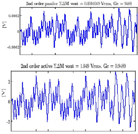
Fig. 8. Loop filter’s output voltages of a 2nd order SD Modulator
Whereas when the noise of the comparator (non-ideal) in a amplifierless modulator is considered its performance is degraded significantly. This is because of high enervation in the loop filter, that converts to a low voltage input to the comparator . Therefore to reduce the comparator noise we can use a pre-amplifier before the comparator.
IV. PROPOSED CT - SD MODULATOR USING PASSIVE RC INTERGRATORS AND INTERSTAGE
LOW GAIN AMPLIFIERS
As discussed earlier, the comparators noise requirements becomes challenging by using passive integrators exclusively to design the loop filter of the modulator, because of the low voltage input to the comparator. In the proposed modulator so as to achieve good effective resolution of 11-bits, a elementary low gain open loop amplifier is inserted amidst each passive RC integrator in a 3rd order modulator.
H1 + H2 + H3
DAC
C2 C3
D out
[image:3.595.59.267.155.316.2]fs Vin
Fig. 9.Block Diagram of the proposed 3rd order 1-bit CT SD Modulator
[image:3.595.54.290.474.660.2]mentioned circuits can be designed for low power dissipation and low power supply voltages. These circuits occupies less silicon area than the high gain and high bandwidth amplifier circuits.
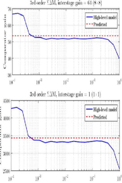
[image:4.595.50.290.183.542.2]The major drawback of his 3rd order modulator is its stability issues and to overcome this and other tradeoffs like non linear behavior of 1-bit quantizer the loop filter will be designed in such a way that optimizes the filter function thereby enhancing the SNDR for a given bandwidth and minimising area.
Fig. 10. Comparator gain vs input signal amplitude of a 3rd order SD Modulator.
The comparator designed fo rthis 3rd order modulator comprises a pre-amplifier, a regenerative latch and a D-flipflop. Pre-amplifier is a simple differential pair with load reisistor, used for reducing the offset voltage and noise of the comparator. Regenerative latch is designed with a pair of PMOS transistor along with a latch which is used to produce the digital output.
1-bit DAC is designed by using a simple CMOS inverters,driving the feedback resistor.
V. PERFORMANCE SUMMARY AND COMPARISION TABLE
VI. CONCLUSION
This paper discussed
About the how the lop gain can be obtained. Only by using a comparator. Here comparator is a 1-bit quantizer.
The limitation of passive only structure is comparator noise and this is because of low input swing at its input.
This issue can be resolved by using a simple differential pair, which acts like a low gain open loop amplifier between each passive RC integrator.
A 3rd order CT SD modulator can be designed that may achieve more than 11-bit effective resolution over a 2 MHz bandwidth.
Genetic algorithm may be used in the proposed modulator to enhance the performance.
Because of the tradeoff among the RC variations and loop stability the modulator is optimized by considering this ill-favoured behaviour, thus circumventing the need for alignment of RC values.
REFERENCES
1. J. M. de la Rosa, “Sigma-delta modulators: Tutorial overview, design guide, and state-of-the-art survey,” IEEE Trans. Circuits Syst. I, Reg. Papers, vol. 58, no. 1, pp. 1–21, Jan. 2011.
2. V. Srinivasan, V. Wang, P. Satarzadeh, B. Haroun, and M. Corsi, “A 20 mW 61 dB SNDR (60 MHz BW) 1b 3rd-order continuous-time delta-sigma modulator clocked at 6 GHz in 45 nm CMOS,” in IEEE Int. Solid-State Circuits Conf. (ISSCC) Dig. Tech. Papers, Feb. 2012, pp. 158–160.
3. S. Zeller, C. Muenker, R. Weigel, and T. Ussmueller, “A 0.039 mm2 inverter-based 1.82 mW 68.6 dB-SNDR 10 MHz-BW CT-ΣO-ADC in 65 nm CMOS using power- and area-efficient design techniques,” IEEEJ. Solid-State Circuits, vol. 49, no. 7, pp. 1548–1560, Jul. 2014. 4. K. Matsukawa et al.,
Published By: single-opamp resonator,” IEEE J. Solid-State Circuits,
vol. 45, no. 4, pp. 697–706, Apr. 2010.
5. T. Song, Z. Cao, and S. Yan, “A 2.7-mW 2-MHz continuous-time OΣ modulator with a hybrid active–passive loop filter,” IEEE J. Solid-State Circuits, vol. 43, no. 2, pp. 330–341, Feb. 2008.
6. J. L. A. de Melo, “A low power 1-MHz continuous-time OΣM using a passive loop filter designed with a genetic algorithm tool,” in Proc. IEEE Int. Symp. Circuits Syst. (ISCAS), May 2013, pp. 586–589.
7. F. Chen and B. Leung, “A 0.25-mW low-pass passive sigma-delta modulator with built-in mixer for a 10-MHz IF input,” IEEE J. Solid- State Circuits, vol. 6, no. 6, pp. 774–782, Jun. 1997.
8. J. L. A. de Melo, F. Querido, N. Paulino, and J. Goes, “A 0.4-V 410-nW opamp-less continuous-time ΔΣ modulator for biomedical applications,” in Proc. IEEE Int. Symp. Circuits Syst. (ISCAS), Jun. 2014, pp. 1340–1343. 9. A. Hussain, S.-W. Sin, C.-H. Chan, S.-P. Ben U, F.
Maloberti, and R. P. Martins, “Active passive ΔΣ modulator for high-resolution and low-power applications,” IEEE Trans. Very Large Scale Integr. (VLSI) Syst., vol. 25, no. 1, pp. 364–374, Jan. 2017. 10. J. L. A. de Melo, J. Goes, and N. Paulino, “A 0.7 V 256
μW ΔΣ modulator with passive RC integrators achieving 76 dB DR in 2 MHz BW,” in Proc. IEEE Int. Symp. VLSI Circuits, Jun. 2015, pp. 290–291.
11. J. L. A. de Melo, B. Nowacki, N. Paulino, and J. Goes, “Design method- ology for sigma-delta modulators based on a genetic algorithm using hybrid cost functions,” in Proc. IEEE Int. Symp. Circuits Syst. (ISCAS), May 2012, pp. 301–304.
12. Joao L.A de Melo, NunoPaulino, Joao Goes, “Continuous time Delta Sigma Modulators based on Passive RC integrators” IEEE Trans. Circuits Syst. I, Reg. Papers, vol. 65, no. 11, Nov. 2018.
13. Susana Patón, Antonio Di Giandomenico, Luis Hernández, Member, IEEE, Andreas Wiesbauer, Member, IEEE, Thomas Pötscher, and Martin Clara “A 70-mW 300-MHz CMOS Continuous-Time ∆∑ADC With 15-MHz Bandwidth and 11 Bits of Resolution,”IEEE J. Solid- State Circuits, vol. 39, no. 7, Jul.2004.
14. Ivan John O’Connell, Member, IEEE, and Colin Lyden, Member, IEEE “A Novel Noise Efficient Feedback DAC Within a Switched Capacitor ∆∑ ADC“, IEEE Trans. Circuits Syst. I, Reg. Papers, vol. 52, no. 1, Jan. 2005. 15. Gil-Cho Ahn, Student Member, IEEE, Dong-Young