International Journal of Innovative Technology and Exploring Engineering (IJITEE) ISSN: 2278-3075, Volume-8, Issue- 9S2, July 2019
Abstract— Compound semiconductor CZTSe is a popular absorber layer for thin film solar cells. Instead of single semiconductor buffer layer, a hybrid buffer layer is used with CZTSe absorber layer. To reduce further usage of toxic materials(CdS) and simultaneously to increase the solar cell efficiency, Ag doped buffer layer was proposed and a numerical studies were performed using SCAPS 1-D simulation programme. Also the thickness and the carrier density of the different layers in the solar cell were optimized to achieve the above goals. After the simulation process, the toxic materials usage was reduced by 62% and the efficiency was increased from 12.24% to 12.69%.
Key words— CZTSe, Ag doping, Buffer layer, SCAPS, Efficiency
1. INTRODUCTION:
The solar photo voltaic energy source is one of the best alternate energy sources at present. The Si-wafer based photo voltaic solar cell is the most popularly used cell but it is not very economic. The thin film solar cell is an economic solution to this problem. Thin film solar cells not only consume less material, its manufacturing process enables large area modules to be made, and does not require high temperature. Thus, the manufacture of thin film solar cells cost much lower than that of Si-wafer based solar cells[1]. The criteria for selecting the solar cell materials are based on availability of process technology, as well as the availability, cost and eco-friendliness of the raw materials. However, thin film solar-cells are less efficient than Si solar cell. In the author’s previous work[2], with CZTSe/CdS/n- ZnO/i-ZnO solar cell, buffer layer thickness was optimized at CdS=65nm, n-ZnO=15nm and an efficiency of 12.24% was obtained using SCAPS simulation program. The goals of this simulation are: i) to increase the efficiency, ii) to reduce the usage of toxic materials, and iii) to reduce overall materials used, using SCAPS simulation program. The following methods have been used to achieve the above objectives, i ) fine tuning the band gap of buffer layer which will in turn improve the carrier generation, ii) fine tuning the thickness of different layers which can improve the carrier generation and reduce recombination, iii) fine tuning the
Revised Manuscript Received on July 18, 2019.
Kajal Mukhopadhyay, Department of Electronics and Communication Engineering, Dayananda Sagar college of Engineering,
Bangalore, Karnataka-560078, India. (E-mail:
P. Fermi Hilbert Inbaraj, Department of Physics, Bharathidasan Institute of Technology (BIT) Campus, Anna University, Tiruchirappalli-620024, India.
J. Joseph Prince, Department of Physics, Bharathidasan Institute of
carrier concentrations to improve carrier generation and reduce recombination.
2. DEVICE MODELLING :
In solar radiation, photons have different energies. Hence solar radiation can be converted more efficiently into electrical energy if different band gap materials are used in solar cell. As the energy of the photon increases, the band gap of the material required to convert it must also increase. Semiconductor with high band gap is placed at the front side as the high energy photons are converted first; consequently, the semiconductor with low band gap is placed at the rear. Based on the above principle, two types of solar cells can be designed : hetero junction and multi-junction. A hetero junction solar cell has been designed in this work. Fig.-1 shows a diagram of the proposed model.
Figure-1: A model of thin film solar cell
i) Window layer:
This layer should be transparent to the incident radiation and conducting enough to collect the charge carrier. i-ZnO has all the required properties for a window layer, including the band gap of 3.3eV [3][12]. Thus, for the window layer, i-ZnO was considered.
ii) Buffer layer:
A solar cell is a p-n junction diode, and the p-type CZTSe is being used as the absorber layer (see 2.(iii)). Thus, an n-type semiconductor layer must be used as the buffer layer. For higher efficiency, the buffer and absorber layers must have their conduction bands aligned[1]. CdS with band gap of 2.4eV was found to be a suitable buffer layer with CZTSe
Efficiency Improvement of CZTSe Solar Cell
with Ag Doped Zno/Cds Buffer Layer, using
Scaps Simulation Programme
USING SCAPS SIMULATION PROGRAMME absorber layer for better band alignment[2]. However, since
CdS is a toxic material, to reduce its usage, some amount of ZnO is added to the buffer layer. This hybrid of ZnO and CdS is used as the buffer layer to improve the overall efficiency. At the front side, closer to the window layer, n-ZnO with band gap of 3.3eV was used and then CdS layer with band gap of 2.4eV was used.
Zinc Oxide is available aplenty in nature and is non-toxic in nature, thus becoming an attractive material for developing the next generation solar cell. It has a stable Wurtzite structure. The following deposition techniques are used to deposit ZnO films: Electrochemical-deposition, CVD (chemical vapour deposition), Radio Frequency magnetron sputtering method, sol-gel, etc[4],[23]. Generally, to adjust the properties of n-ZnO/CdS, doping with noble metals like Ag and Au are used[6]. The ionization energy of Ag is less than Au, hence Ag was used for doping ZnO/CdS[5]. With the increase of Ag concentration in ZnO, the absorption band edges shifted to longer wavelengths which means there is a decrease in the band gap of the ZnO after doping with Ag[4],[5].With the increase in Ag at 10.3wt%, the band gap reduced from 3.28eV to 2.65eV; the band gap decreases with further doping[7]. Minority carrier concentration at equilibrium decreases with increase in doping density. So if we increase the doping density, minority carrier concentration decreases and open circuit voltage increases. At the same time, high doping density increases carrier recombination which reduces Voc. The doping density of the absorber and buffer layers need to be optimized to obtain maximum open circuit voltage.
The optical properties of Ag doped CdS thin film made using the spray pyrolysis process were studied by M. A. Khalid et al., who reported that with the variation of doping concentration range (0-2.5) wt% the energy gap varies from 2.4eV to 2.21eV[8]. Shubham Chandel et al. reported that, the band gap of CdS was reduced from 2.49eV to 2.33eV after Ag doping[10]. Ag acts as an acceptor dopant and reduces the band gap of CdS. Sergio R. Ferra-Gonzalez had studied how the band gap of CdS thin film varies with changing concentration of Ag. CdS was deposited in a chemical bath as thin films and doped with Ag. Here, the band gap variation lay between 2.31 and 2.51eV[11]. In this pioneering work, Ag doped CdS/ZnO hybrid buffer layer was used for fine tuning the band gap.
iii) Absorption layer:
Copper Zinc Tin Selenium (Cu2ZnSnSe) is an ideal material to use as an absorption layer. It has a suitable band gap of 0.95eV, it is an eco-friendly material, and all the constituents of CZTS are available in plenty at a low cost[26]. The manufacturing process is also cost
effective[3]. CZTSe has a high absorption coefficient because electron-hole pair generation is more probable, as the bottom of the conduction band and the top of the valence band match. The carrier mobility and carrier life time is also high for CZTS. Between the kesterite and stannite phases of CZTS, the former phase is more stable. In the CZTS crystal structure there are mainly Zn vacancies and Cu atoms occupy the Zn vacancy sites, thus making it a p-type material. The Cu/Zn ratio can be varied in order to control the conductivity of this layer.
3. SCAPS
One dimensional solar cell can be simulated by Solar cell capacitance simulator (SCAPS). Poisson equations and continuity equations are solved in this simulation programme. The electrical parameters such as: open circuit voltage (Voc), short circuit current (Isc), fill factor (FF), capacitance voltage spectroscopy, quantum efficiency, generation and recombination profiles and carrier current densities are calculated at different temperatures. Other parameters, such as dielectric constant, refractive index, absorption constant, etc., are also used in this simulation process. Parameters of particular interest are the band to band recombination, defects and interface thickness, series and shunt resistance of the cell. A maximum of seven semiconductor layers with front contacts and back contacts can simulated in SCAPS. The specification parameters of the materials associated with each solar cell layer are given as input to the simulation program [13], [14].
4. DEVICE SIMULATIONS
International Journal of Innovative Technology and Exploring Engineering (IJITEE) ISSN: 2278-3075, Volume-8, Issue- 9S2, July 2019
Table-1: Bandgap, layer thickness and carrier density of the solar cell materials
Parameters Unit CZTSe ZnO CdS i-ZnO
1.Band gap eV 0.95 3.3 2.4 3.3
[2][25] 2.Thickness ( uniform layer) nm 2600 Total thickness 80 40
3.Uniform Acceptor/ Donor
density cm
-3
1000E+16 1.00E+17 1.00E+17 5.00E+17 Set-1 1000E+17 1.00E+18 1.00E+18 5.00E+17 Set-2 1000E+17 1.00E+17 1.00E+18 5.00E+17 Set-3
5. RESULTS:
In Fig.2, the ZnO- thickness is on the x-axis (unit: 20nm), CdS- thickness is on the y-axis (unit: 20nm) and solar cell efficiency is on Z-axis (relative to 12%). Five combinations of ZnO/CdS thickness: 80/0, 60/20, 40/40, 20/60 and 0/80, were considered for each set as mentioned in Table-1. The results are shown in red, blue and yellow for sets 1, 2 and 3 respectively, of different carrier densities shown in the Table-1 .
The simulation was done in five steps.
i) Step-1: The simulation results in Fig-2 shows that the set-3 has has higher efficiency for all the thickness combinations of buffer layers.
Fig-2 : Efficiency variations with different buffer layer combinations(with out Ag)
ii) Step-2: The ZnO buffer layer was replaced by Ag doped ZnO. S.M. Hosseini et al. reported that for Zn 1-xAgxO nano crystals with x=0.07, the band gap is reduced from 3.3eV to 3.18eV[5] and the thus band gap of ZnO was considered as 3.18eVfor this simulation. The results are shown in Fig-3. The efficiency of solar cell with Ag doped ZnO is higher when compared to ZnO without Ag, for all the three sets and for all the ZnO/CdS buffer layer thickness combinations. The results also show that the efficiency is higher for set-3 compared to set-1 and set-2. Additionally, the variation in the efficiency of ZnO/CdS
combinations are very less for set-3. The maximum efficiency of 12.63% is obtained for ZnO=60nm and CdS=20nm for set-3 .
Fig-3 : Efficiency variations with different buffer layer combinations(with Ag)
iii) Step-3: The donor and acceptor density values from set-3 were used for this step of simulation, with the buffer layer thickness of ZnO=60nm and CdS=20nm. To observe the changes in efficiency with change in the thickness of the window layer, three values of i-ZnO thickness were used: 20, 30 and 40nm, for which the efficiencies obtained are12.69%, 12.66% and12.63% respectively. The maximum efficiency of 12.69% was obtained for the 20nm window layer and this value was used in the next step.
iv) Step-4:To reduce further material usage, a simulation was performed with ZnO=40nm and the same result was obtained as with ZnO=60nm. Hence the n-ZnO buffer layer thickness of 40nm was used in the next step.
v)Step-5: Ag doped CdS was considered as the buffer layer for simulation, with CdS band gaps of 2.3eV and 2.49eV. The efficiency obtained was 12.69% for buffer layers made of both the Ag-doped and normal CdS. Hence normal CdS was finalized for the buffer layer to avoid unnecessary doping. Table-3 thus compares the parameters used in the initial model and those used in the final model.
Table-3: A comparison between Initial Model and Final Model
Layer Material Parameter Initial Model
(ƞ=12.23%)
Final Model (ƞ=12.69%)
1. i-ZnO Thickness(nm) 40 20
Band gap(eV) 3.3 3.3
USING SCAPS SIMULATION PROGRAMME
2. n-ZnO Thickness(nm) 15 40
Band gap(eV) 3.3 3.18
Carrier density(cm-3) 1000E+17 1000E+17
3. n-CdS Thickness(nm) 65 20
Band gap(eV) 2.4 2.4
Carrier density(cm-3) 1000E+17 1000E+18
4. p- CZTS Thickness(nm) 2600 2600
Band gap(eV) 0.95 0.95
Carrier density(cm-3) 1000E+16 1000E+17
6. ANALYSIS:
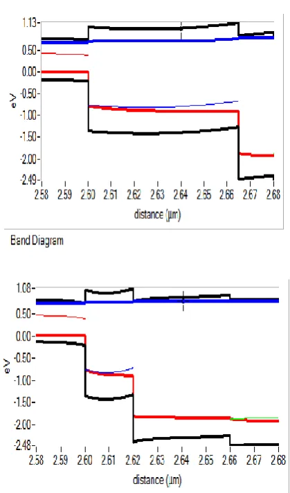
i) Band diagram :
[image:4.595.59.269.354.710.2]Band diagram for the initial model and final model are shown in Fig4a and Fig. 4b respectively. In Fig 4a from, 0 to 2.60μm is CZTS layer and from 2.60μm to 2.665μm is CdS layer. In Fig 4b, from 0 to 2.60μm is CZTS layer and from 2.60μm to 2.62μm is CdS layer. In both graphs, the conduction band offset at CZTSe/CdS junction is 0.3eV, where the maximum band offset requirement for achieving high efficiency is 0.4eV[2][24].
Fig 4a : Band diagram for the initial model Fig4b: Band diagram for the final model Ec and Ev -black
line. EFp -red line, EFn -blue line
ii) Generation/recombination profile:
In Fig 5a, the generation/recombination profile for the initial model and in Fig 5b the generation/recombination profile for final model are shown. The e-h generation (green line) and the net generation of electrons and holes (red line) are higher in the final model compared to the initial model.
Fig5a: Gene./recomb. Profile for the initial model Fig5b: Gene./recomb profile for the final model
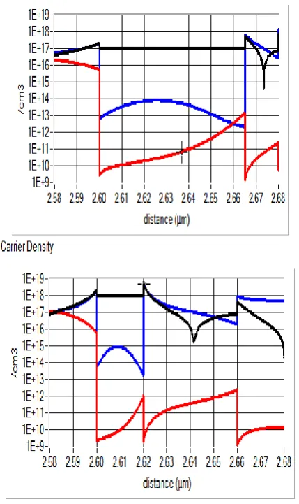
iii) Carrier density:
International Journal of Innovative Technology and Exploring Engineering (IJITEE) ISSN: 2278-3075, Volume-8, Issue- 9S2, July 2019
Fig 6a: Carrier density for the initial model Fig 6b: Carrier density for the final model
7. CONCLUSION:
The simulation was started with the parameters given in the initial model and finished with the parameters given in the final model. By using Ag doped n-ZnO layer, fine tuning the acceptor/donor density and optimizing the buffer layer thickness, three positive improvements were obtained: i) CdS layer thickness was reduced from 65nm to 20nm, a 62% reduction in usage of toxic material , ii) Efficiency increased from 12.24% to 12.69% , iii) Total thickness was reduced by 40nm.
8. REFERENCE:
1. Chetan Sink Solanki, Solar Photovoltaivic- Fundamentals,Technologies and applications, second editions, PHI, ISBN no. 978-81-203-4386-3.
2. Kajal Mukhopadhyay, P. Fermi Hilbert Inbaraj and J. Joseph Prince .Thickness optimization of CdS/ZnO buffer layer in CZTSe thin film solar cells using SCAP simulation program. Material Research and Innovation. http://doi.org/10.1080/14328917.2018.1475907.
3. O. K. Simya et al: “A comparative study on the performance of kesterite based thin film solar cell using Scaps simulation program”: superlattices and microstructures 82(2015) pp248-261.
4. Fenglin Xiang et. al. : “Characterization of Ag doped ZnO thin film synthesized by sol gel method and its using in thin film solar cell”, Optik 124(2013) 4876-4879.
5. Hosseini et.al : “Effect of Ag doping on structural, optical and photo catalytic properties of ZnO nanoparticles”: Cond-mat.mtrl-sci arXIV: 1508.000382V, 2015.
6. M.Karyaoui, A. Mmhamdi, H.Kaouach, A. Labidi, A. Boukhachem, K.Boubaker, M. Amlouk, R. Chtourou., Some physical investigation on silver- doped ZnO sprayed thin films, Material science in semiconductor processing, 30(2015) pp-255-262.
7. Mangesh Lenjwar et.al. : “Enhanced performance of Ag doped ZnO and pure ZnO thin film DSSCs prepared by solgel spin coating” , Inorganic and nonmetal chemistry 2017 vol 47 , no.7, 1090-1096
8. M.A. Khalid and H.A.Jassem, “Electrical and optical properties of polycystalline Ag-doped CdS thin films”, Acta Physica Hungarica, 73(1) pp 29-34,1993
9. H. Katagiri, K.Jimbo, W.S.Maw,K. Oishi, M. Yamazaki, H. Araki,A.Takeuchi, Development of CZTS based thin film solar cell, Thin Solid films, vol 517,issue 7, 2009,pp 2455-2460.
10. Shubam Chandel, Ajan P.R, Annie Joseph V, V P N Nampoori, P Radhakrishnan, “A study of CdS and Ag doped CdS prepared through CBD technique”, International conference on fiber optics and photonics, optical society of India 2012.
11. Sergio R. Ferra-Gonzalez et al, “Optical and structural properties of CdS thin films grown by chemical bath deposition doped with Ag by ion exchange”, Optik 125(2014) 1533-1536.
12. Anant H. Jahagirdar, Ankur A. Kadam and eelkanth G. Dhere.” Role of i-ZnO in optimizing open circuit voltage of CIGS2 and CIGS thin film solar cell”, Proceedings of the Conference Record of the 4th IEEE World Conferenceon Photovoltaic Energy Conversion, 2006, pp.557–559.
13. Marc Burgelman, Koen Decock, Alex Niemegeers, Johan Verschraegen, Stefaan Degrave -SCAPS manual. Version: 17 February 2016
14. M. Burgelman, P. Nollet, S. Degrave, “Modelling polycrystalline semiconductor solar cells”, thin solid film, 361-362(2000) pp. 527-532
15. Abdelbaki Cherouana, Rebiha Labbani: “Study of CZTS and CZTSSe solar cell for buffer layer selection”: Applied Surface Science, 4 May 2017
16. Springer handbook of electronic and photonic materials, ISBN 0387-26059-5.
17. Sudipto Saha et al, “Performance of CZTSSe Solar cell with various Mole fractions of Sullfur for different buffer layers”, 4th ICDRET, Jan-2016.
18. Atul Kumar and Ajay D. Thakur, “Analysis of SnS2 buffer layer and SnS back surface layer based CZTS solar cells using SCAPS”, Research gate publications/283043296, Oct-2015.
19. Darvish Zadesh P, Sohrabpoor H, Gorji NE. Numerical device simulation of carbonnanotube contacted CZTS solar cells. Opt Quant Electron. Oct 2016; 48-480.
20. Sudipto Saha, Ramiraj C.Shahidul Hassan, “ Improvement of the Output Performance of CZTS Thin Film Solar Cell” 2nd International Conference on Electrical, Computer & Telecommunication Engineering (ICECTE),2016,Dec,Rajshai.
USING SCAPS SIMULATION PROGRAMME 22. Abu Shama Mohammad Miraz, Md. Mortuza Faruk and
Muhammad Asad Rahman. “Numerical Analysis of Deep Level Defects in Cu2ZnSnS4 (CZTS) Thin Film Solar Cells “: 2015 3rd International Conference on Green Energy and Technology (ICGET)
23. Y. Sanchez et al. “ Advanced hybrid buffer layers for CZTS solar cells”, Conference paper: 978-1-5090-2724-8/16/ ©2016 IEEE ,pp 1511-1515
24. T. Minemoto et al. “Theoretical analysis of the effect of conduction band offset of window /CIS layer on performance of solar cell using device simulation”, Solar energy materials and solar cells, 67(2001) 83-88.
25. Rafee Mahbub et al, “ Simulation of CZTS thin film solar cell for different buffer layer for high efficiency performance”, SAJET, vol2, no 52(2016), 1-10.
26. Omar A.M. Abdelraouf, Nagesh K Allam: “Nanostructuring for enhanced absorption and carrier collection in CZTS based solar cells: coupled optical and electrical tunneling”: Optical materials 54(2016) pp 84-88. 27. Hong Zhang, Shuying Cheng, Jinling Yu, Haifang Zhou,
![3 [(2 Chloro 1,3 thiazol 5 yl)methyl] 5 methyl 1,3,5 oxadiazinan 4 one](data:image/gif;base64,R0lGODlhAQABAIAAAP///wAAACH5BAEAAAAALAAAAAABAAEAAAICRAEAOw==)