City, University of London Institutional Repository
Citation
:
Constantinou, L., Triantis, I., Bayford, R. & Demosthenous, A. (2014).
High-power CMOS current driver with accurate transconductance for electrical impedance
tomography. IEEE Transactions on Biomedical Circuits and Systems, 8(4), pp. 575-583. doi:
10.1109/TBCAS.2013.2285481
This is the accepted version of the paper.
This version of the publication may differ from the final published
version.
Permanent repository link:
http://openaccess.city.ac.uk/14321/
Link to published version
:
http://dx.doi.org/10.1109/TBCAS.2013.2285481
Copyright and reuse:
City Research Online aims to make research
outputs of City, University of London available to a wider audience.
Copyright and Moral Rights remain with the author(s) and/or copyright
holders. URLs from City Research Online may be freely distributed and
linked to.
City Research Online:
http://openaccess.city.ac.uk/
[email protected]
Abstract—Current drivers are fundamental circuits in
bioimpedance measurements including electrical impedance tomography (EIT). In the case of EIT, the current driver is required to have a large output impedance to guarantee high current accuracy over a wide range of load impedance values. In this paper we present an integrated current driver which meets these requirements and is capable of delivering large sinusoidal currents to the load. The system employs a differential architecture and negative feedback, the latter allowing the output current to be accurately set by the ratio of the input voltage to a resistor value. The circuit was fabricated in a 0.6-μm high-voltage CMOS process technology and its core occupies a silicon area of 0.64mm2. It operates from a ±9V power supply and can deliver output currents up to 5mA pk-pk. The accuracy of the output current is within 0.41% up to 500kHz, reducing to 0.47% at 1MHz for currents up to 5mA pk-pk with a total harmonic distortion of 0.69%. The output impedance is 665kΩ at 100kHz and 372kΩ at 500 kHz.
Index Terms—Accurate transconductance, bioimpedance,
CMOS circuits, current driver, electrical impedance tomography (EIT), high power design.
I. INTRODUCTION
LECTRICAL IMPEDANCE TOMOGRAPHY (EIT) offers particular promise in the assessment of neonatal lung function because it is as a non-invasive imaging method requiring no collaboration from the infant [1]-[4]. Sinusoidal currents are applied to the surface of the body tissue via electrode pairs and the resulting surface potentials are recorded at several locations of the electrode array in order to obtain a set of bioimpedance measurements. Specialized reconstruction algorithms are then employed to produce a
Manuscript received April 8, 2013. This work was supported by the UK Engineering and Physical Sciences Research Council (EPSRC) under grant EP/G061629/1.
L. Constantinou and A. Demosthenous are with the Department of Electronic and Electrical Engineering, University College London (UCL), London, WC1E 7JE, U.K. (email: [email protected]; [email protected]).
I. F. Triantis is with the Department of Electrical and Electronic Engineering, City University, London, EC1V 0HB, U.K. (e-mail: [email protected]).
R. Bayford is with the Department of Health and Social Sciences, Middlesex University, The Burroughs, London, NW4 4BT, U.K. (e-mail: [email protected]).
tomographic image [5]. The high air content of the lung can provide high contrast images as the impedance of the air is much higher than the surrounding tissue. Absolute lung resistivity can be associated with structural characteristics and tissue composition which can be useful in the identification of certain health conditions in neonatal lungs [4].
Current drivers are key devices in EIT systems. For accurate current delivery to the tissue load a current driver should have high output impedance over the total bandwidth of operation. In the case of neonatal lung function monitoring the frequency range is typically 4kHz to 813kHz [4] and an output current accuracy of better than 0.5% is desirable. In practice the impedance of the load (electrode-tissue interface) can vary greatly in magnitude. A study of the electrode-tissue impedance characteristic was presented in [6], in which six different types of Ag/AgCl electrodes were evaluated over the frequency range between 10 Hz and 1 MHz. For frequencies below 1 kHz the electrode-tissue impedance was higher than
10 kΩ and reduced to approximately 1.7kΩ at 10kHz, 800Ω
at 50kHz, 559Ω at 100kHz, and 494Ω at 1MHz. In another
study [7], electrode-tissue impedance characteristics were
reported to be around 220Ω at 100kHz reducing to 120Ω at
1MHz. Exact determination of the load impedance is a
difficult task, thus when dealing with the design of bioimpedance instrumentation a range of load values need be considered.
The majority of current drivers reported in the literature for EIT and bioimpedance applications are based on discrete electronic designs mostly employing the modified Howland topology [8]. A balanced Howland topology uses a pair of opamps and resistive networks in positive and negative feedback paths. The performance of the Howland topology depends on the specification of the opamps used and the degree of matching of the resistors. The design in [9] used resistors of 0.01% tolerance in order to achieve a high output
impedance (1.7MΩ at 50kHz). The Howland topology in
[10] achieved a measured output impedance of about 750kΩ at 10kHz, reducing to 330kΩ at 300kHz, and eventually to
70kΩ at 1MHz. The maximum output current was limited to
1mA pk-pk with an accuracy of about 2% over the total bandwidth. The need for extremely high resistor precision makes the Howland topology unsuitable for integrated circuit design.
High-Power CMOS Current Driver With
Accurate Transconductance for Electrical
Impedance Tomography
Loucas Constantinou, Iasonas F. Triantis,
Member, IEEE
, Richard Bayford,
Member, IEEE
, and
Andreas Demosthenous,
Senior Member, IEEE
measured output impedance of 2.6MΩ at 100kHz reducing to
160kΩ at 500kHz. The current driver in [12] uses an opamp
in inverting configuration with the load present in the negative feedback path. Particular attention was again given to the output impedance characteristic of the circuit and its dependency upon the circuit’s components. It achieved a
measured output impedance of about 350kΩ at 50kHz
reducing to 120kΩ at 1MHz. The EIT system in [13] used a
current conveyor based current driver, with a measured output
impedance of 1.5MΩ at 10 kHz, reducing to 29.7kΩ at
500kHz. A dc suppression feedback loop was utilized to keep
the dc output voltage levels to zero. The instrumentation amplifier (IA) based current driver in [14] used digitally-controlled negative capacitance circuits to regulate the circuit’s output capacitance and resistance and thus trim the overall output impedance at a specific operating frequency. After trimming the measured output impedance was above
64MΩ at 30kHz but temperature variations caused it to drift
to below 25MΩ.
A handful of custom integrated current drivers have been presented [15]-[19]. The design in [15] is a modification of the supply current sensing scheme [11] using bipolar technology. Simulated results indicated that the circuit’s output impedance is 2.5MΩ at 1MHz but no measurements to date have been reported. A current driver in 0.18-µm CMOS technology was described in [16] using four current sources implemented in an H-bridge configuration. The circuit uses common-mode feedback (CMFB) to control the dc voltage levels at the output nodes. It achieved high output impedance in simulation
(10.2MΩ at 1MHz) but no measurements were reported. The
current driver in [17] also uses a standard 0.18-µm CMOS
technology. It was designed to operate at 90kHz and uses two
fully differential amplifiers to generate the input sinusoidal voltage signal, cascaded by a voltage controlled current source implemented by two transistors and a resistor. Its maximum
output current is only 350µA pk-pk with an accuracy of 1% at
90kHz. The integrated current driver presented in [19] is based on an open loop operational transconductance amplifier (OTA) with an active inductive load. It was reported to
achieve an output impedance in excess of 500kΩ at 500kHz
but its maximum output current is limited to 500µA pk-pk.
We are working on the development of a parallel current drive EIT system with “active” electrodes, primarily for neonatal lung function imaging [1], [5]. The encapsulation of the current driver (and impedance measurement circuitry) within the electrode shell removes lead capacitance problems and therefore enables fast, accurate impedance measurements at relatively high frequencies [20], [21]. A wearable active vest which contains a collection of active electrodes is being developed [22]. Our application requires current drivers with accurate transconductance and capable of generating currents up to 5mA pk-pk with good accuracy (<0.5%) over a wide
frequency rage (≤1MHz). Using custom integrated circuit
techniques allows for system miniaturization and potentially better performance than discrete implementations [19]. In [23]
we presented the preliminary design of a high power CMOS current driver employing negative feedback (see Fig. 1). The
negative feedback allows to accurately set the
transconductance of the current driver through the value of the sense resistor Rs, and also regulates the current through the
load thus enhancing the overall output impedance. This paper is an expansion of [23] where we present the complete design and test results of the fabricated current driver chip implemented in a 0.6-µm high-voltage (HV) CMOS process technology. The rest of the paper is organized as follows. Section II outlines the system architecture and circuit operation. Section III describes the circuit design of the system blocks. Section IV examines the frequency response and compensation using a small-signal equivalent model of the designed current driver circuit. Section V presents measured results from the fabricated chip samples. The concluding remarks of Section VI complete the paper.
II. SYSTEM ARCHITECTURE
Figure 1 shows the system block diagram of the current driver topology in which two identical single-ended feedback current drivers operate in balanced mode to minimize common mode voltage errors across the load (Zload). Each current driver
consists of a preamplifier stage (A1, A2) followed by a
transconductance stage (Gm1, Gm2). The current through the
load is sensed via two integrated resistors (Rs1, Rs2) and the
resulting voltage is fed back to the negative input terminal of the preamplifier thus establishing a negative feedback path. Two voltage buffers (B1, B2) present in the feedback loop
measure the voltage across the sense resistor and also isolate the load from the input signal. The output current is generated via a differential input voltage through which both current drivers receive 180º shifted signals (Vin1, Vin2) thus each one is
either sourcing or sinking current relative to the other.
Assuming a resistive load (RL) the low frequency
transconductance of a single current driver is given by
M19 M18
M17 M16
M1 M2
M21 M20 M4 M10
M
3
B
M
3
A
M6
M7 M9
M12
M13 M15
M25 M24
M23 M22
M30A
M27 M26
M29 M28
M30B VSS
Vi2+ Vi2–
Ibias2
Vb4
Vb5 Vb5
Vb4 VDD
VSS
Vo2– Vo2+
VSS Ibias1
Vi1+ Vi1– Vo1+
Vo1–
Vb1 Vb2 Vb3
M12
M14 M11
M13 M3
M1 M4
M2 M7
M5 M8
M6
(a) (b)
VDD
1a 1b
4a
3a
4b 2a 2b
3b
[image:3.612.315.562.53.229.2]Io+ Io–
s m o
L s o
m L
R
AG
r
R
R
r
AG
V
I
G
in
driver (1)
where IL is the load current, A is the voltage gain of the
preamplifier, Gm is small-signal gain of the transconductance
stage, ro is the small-signal output resistance of the
transconductance stage, and Rs is the sense resistor. If
ro>>Rs+RL and AGmRs>>1 then Gdriver≈1/Rs. Hence, if the
above conditions are met, Gdriver can be set according to the
value of the sense resistor and thus be independent of the circuit’s internal parameters. The total transconductance of the topology in Fig. 1 is twice the transconductance of a single current driver. The single current driver’s output resistance is given by
s o m
o
G
r
R
r
R
out
(
1
)
. (2) The use of negative feedback therefore enhances the circuit’s output resistance. The system’s total output resistance is halved as the two current drivers are connected in parallel.III. CIRCUIT DESIGN
A. Preamplifier
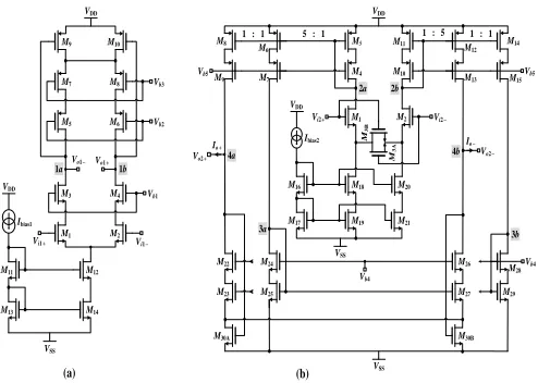
The preamplifier provides an enhancement to Gdriver. Fig.
2(a) shows the schematic diagram of the preamplifier in which a fully differential cascode topology is used. A cascode current mirror formed by transistors M11-M14 provides the
input bias tail current to the input pair differential pair formed by M1 and M2. Transistors M3-M8 provide active loading to the
input differential pair thus enhancing the circuit’s output resistance and differential gain. Bias voltages Vb1-3 are applied
to the cascode pairs to ensure they are operating in the saturation region. All transistors are operating in the saturation region except from M9 and M10 which operate in the triode
region. Their purpose is to provide a CMFB path to stabilize the dc voltage level at the output [24]. Any drifting of the output dc level is compensated by a change in the voltage across these two triode transistors which effectively act as resistors. The value of the resistance is a function of the transistor’s geometry and gate-source voltage. A small change in the output dc voltage level is sensed at the gate of M9 and
M10 whose resistance value changes, thus changing the voltage
drop across them as the quiescent current flowing is constant. This change in the voltage drop across them is in a direction so as to oppose the change in the output dc voltage level. Transistor dimensions were calculated for minimum overdrive voltage consumed by the devices with a quiescent current of
500µA. The preamplifier’s nominal open loop differential
gain and –3dB bandwidth are 816V/V and 2.76MHz,
respectively.
B. Transconductance Stage
Figure 2(b) shows the schematic diagram of the transconductance stage. The architecture is based on a pseudo differential balanced scheme. Transistors M1-M2 biased by
current sources M19 and M21 form the input differential pair
whose linearity characteristic is enhanced by the degeneration pair formed by M3A and M3B. High swing cascode current
mirrors formed by transistors M4-M8, M10-M15 and M22-M29
provide an increased output resistance and a reduced overdrive voltage compared to their regular cascode counterpart. Transistors M30A and M30B operate in the triode region and
stabilize the output dc voltage levels as described in the preamplifier circuit. The current (single-ended) at the output
M19 M18
M17 M16
M1 M2
M21 M20 M5
M4
M11
M10
M3
B
M
3
A
M6
M7 M8
M9
M12
M13
M14
M15
M25 M24
M23 M22
M30A
M27 M26
M29 M28
M30B VDD
VSS
Vi2+ Vi2–
Ibias2
Vb4
Vb5 Vb5
Vb4 VDD
VSS
Vo2– Vo2+
1 : 5
VSS Ibias1
Vi1+ Vi1–
Vo1+
Vo1–
Vb1 Vb2 Vb3
M12
M14 M11
M13
M3
M1
M4
M2
M9 M10
M7
M5
M8
M6
(a) (b)
5 : 1
VDD
VDD
1a 1b
4a
3a
4b
2a 2b
3b
Io+ Io–
1 : 1 1 : 1
[image:4.612.55.560.54.331.2] [image:4.612.92.243.364.403.2]node (Vo2) is the difference between the current supplied by
the PMOS and NMOS current sources. It can be approximated by Io≈BGmi(Vi2+–Vi2–) where B (=5 here) is the current
mirror gain factor between M5 and M6, M8 (or M11 and M12,
M14) as shown in Fig. 2(b), and Gmi is transconductance of the
source degenerated input stage (M1, M2, M3A, M3B). The dc
bias current (Ibias2) is 500µA and the circuit achieves a
maximum output current amplitude of 5mA, thus ensuring the
2.5mA pk-pk required output lies within the circuit’s linear region of operation.
The output voltage compliance of the transconductance circuit in Fig. 2(b) determines the maximum load that the current driver can drive with the maximum output current
amplitude of 2.5mA. However, the allowable injected current
amplitude must comply with international safety standards
[25]. For frequencies less than 1kHz were the load magnitude
is of the order of 10kΩ, the maximum allowable current is
around 100µA, which translates to an output voltage
compliance of about 2V. Current amplitudes of 2.5mA are allowed at frequencies higher than 25kHz where the load
magnitude is reduced to approximately 1kΩ, therefore
requiring an output voltage compliance of 5V. The current driver’s output voltage compliance (Vout) is determined by the
effective compliance of the transconductance stage [Fig. 2(b)]. It is given by
13 12
26 26
30 out DD
SS
V
MV
ovMV
ovMV
V
V
ovMV
ovMV
B
.(3)where VSS and VDD are respectively the positive and negative
supply voltages, VovMi is the overdrive voltage of transistor Mi,
and VM30B is the voltage across M30B.
Transistor dimensions were adjusted in order to maximize output voltage compliance. The output voltage compliance is approximately 15V (some nonlinearities exist near the limits as transistors enter the triode region). This voltage compliance can accommodate a wide range of load impedances, hence making the current driver suitable for a variety of EIT
applications. The transconductance stage was designed for a
nominal gain of 5.6mA/V and a –3dB bandwidth at
approximately 13MHz when the outputs are short-circuited.
C. Voltage Buffer
The purpose of the voltage buffer is to provide a measure of the injected current to the electrode-tissue load by measuring the voltage across the sense resistor (Rs). The measured
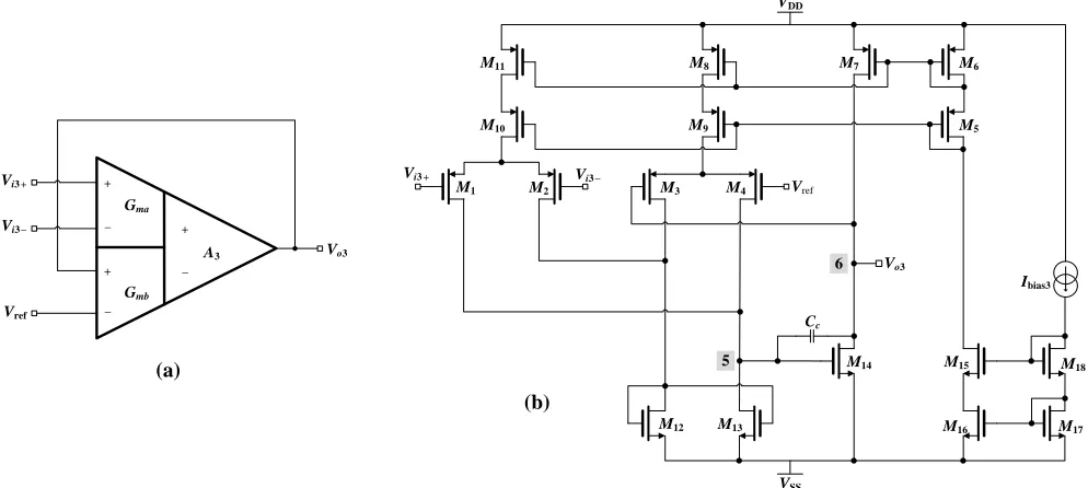
voltage is fed back to the negative input terminal of the preamplifier thus forming a negative feedback loop. As shown in Fig. 1 the voltage buffer is a differential to single ended architecture and the most common topologies are IAs [26], [27]. However, the gain of an IA is typically the ratio of two resistors which have to be tightly matched (for unity gain). To avoid the use of tightly matched resistors the design used a differential difference amplifier (DDA) [28] configured as a differential to single ended unity gain voltage buffer [see Fig.
3(a)]. The DDA features two transconductance elements (Gma,
Gmb) followed by an amplification stage (A3). Input to the
structure is via the input terminals of the top transconductor. The output terminal is fed back to the positive terminal of the bottom transconductor while the negative terminal is held at a constant reference level (Vref) which is set to 0V. The negative
feedback configuration follows the difference between terminals Vin+ and Vin–, which are connected across the sense
resistor terminals as shown in Fig. 1. The schematic diagram of the voltage buffer is shown in Fig. 3(b). Transistors M1-M4
form the two input transconductors biased by current sources
M8 and M11. A second amplification stage is formed by
transistors M7 and M15. NMOS current mirror pair M12 and M13
performs the differential to single ended operation required for the subtraction of the four inputs. The output node is fed back to the gate of transistor M3 for unity gain and a reference
voltage set at 0V is applied to the gate of M4. A 1pF
compensation capacitor (Cc) is added for improved phase
margin.
The voltage buffer’s small signal voltage gain is given by
M1 M2
M10
M11
M9
M8 M7
M3 M4
M6
M5
M14
M13
M12
M15
M16
M18
M17
Ibias3
Vi3+ Vi3–
Vref
Vo3
Cc
VSS
+
_
+
_
+
_
Vo3
Vi3+
Vi3–
Vref
A3
Gma
Gmb
(a)
(b)
5
6
[image:5.612.58.555.55.278.2]14 13 1 7 14 13 13 4 1 14 13 1 ) ( )
( o o o m o o m m m
m m m v g g g g g g g g g g g g A
(4)
where gmi and goi are respectively the small-signal
transconductance and output conductance of transistor Mi. The
circuit achieves a gain of 0.9958V/V at dc and is reduced to
0.9946V/V at 1 MHz.
IV. FREQUENCY COMPENSATION
In order to ensure stability in the negative feedback loop the loop phase response must not exceed the 180º point. The closed-loop transfer function of a negative feedback system is given by f s A s A s T ) ( 1 ) ( ) ( (5)
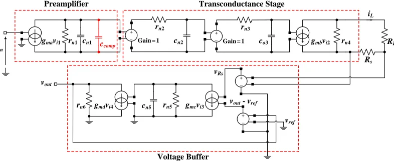
where the term A(s)f is the feedback loop gain. When the phase of the feedback loop becomes –180º at the unity gain frequency of the system, then A(s)f=–1, and the denominator in (5) becomes zero causing the closed loop transfer function to become infinity. Thus, the system becomes unstable and the output oscillates with increasing amplitude. In order to examine the feedback loop response of our system, a simplified small-signal equivalent circuit of a single current driver was constructed and simulated to verify its performance relative to the transistor-level design. The simplified small-signal equivalent circuit is shown in Fig. 4 with the feedback
loop open1. Only capacitances associated with dominant poles
are showed as the rest take place at much higher frequencies and do not affect the frequency performance of the system. In the preamplifier [Fig. 2(a)] the dominant poles occur at nodes 1a and 1b, in the transconductance stage [Fig. 2(b)] at nodes 2a, 2b, 3a and 3b, and in the voltage buffer [Fig. 3(b)] at node 5, the latter forming pole p5. Nodes 1a and 1b carry signals
with the same amplitude but opposite phase. Therefore, nodes 1a and 1b form one single pole p1. The same applies to node
pairs (2a, 2b) and (3a, 3b) in the transconductance stage, forming poles p2 and p3, respectively. In the small-signal
model rni and cni represent the resistance and capacitance of
1 The feedback loop was broken and the negative input of the preamplifier
was set to a dc level that matches the output dc level of the voltage buffer which was almost 0 V.
node ni, respectively. The terms gma and gmb denote the
small-signal transconductance of the preamplifier and the transconductance stage, respectively. The terms gmc and gmd
denote the small-signal transconductance of the voltage buffer’s input stage and output stage, respectively. The values of the small-signal parameters were obtained using the extracted values from the transistor level circuit in Cadence. The resistances RL and Rs were set to 1kΩ and 500Ω,
respectively.
The system’s loop gain transfer function is given by
)
( 5 5 6
3 2 1 6 5 1 n n md mc s n n n md mc mb ma in out r r g g p p p p R r r r g g g g v v
. (6)
The position of the four poles p1, p2, p3, and p5 of the
uncompensated loop gain were evaluated at fp1=916kHz,
fp2=13.26MHz, fp3=205.8MHz, and fp5=13.55MHz, and
the unity gain frequency point at approximately 53MHz. Pole
p3 could be neglected as it takes place at a very high
frequency, yielding a three-pole system. Poles p2 and p5 take
place at really close frequency points. This results in an excess of 180º phase shift as p2 and p5 take place before the unity
gain frequency point thus causing system instability. Placing a
capacitor (ccomp) between the preamplifier and the
transconductance stage provides dominant pole compensation. A 60 pF compensation capacitor created a dominant pole at
approximately 7kHz yielding sufficient phase-margin for
stability in practice.
V. MEASURED RESULTS
The current driver was designed and fabricated in a 0.6-µm CMOS HV process technology [29]. The design and layout were performed with Cadence software. Each of the two on-chip sense resistors were chosen to be 500 Ω, yielding a
nominal Gdriver value of 4 mV/A. The fabricated chip
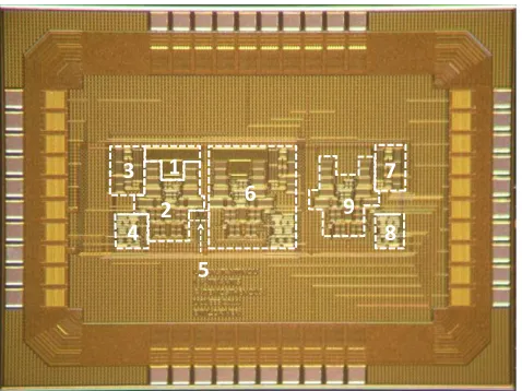
microphotograph is shown in Fig. 5 with the main components numbered. The size of the core area is 0.64mm2.The total chip area including pads and test structures is 6.18mm2. The tests performed aimed to study the circuit’s transconductance (Gdriver) over the required input voltage range as well as the
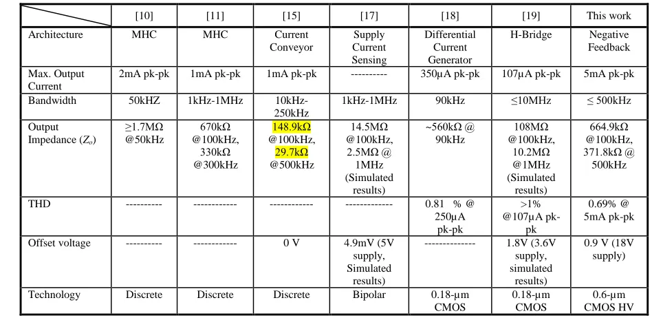
accuracy of the output current over frequency. Other parameters such as output impedance, total harmonic distortion (THD) and input/output phase were evaluated and are reported in Table I. All of the eleven chips operated
_ +
_ +
vin
gmavi1 rn1 cn1 Gain=1 co3 gmbvi2 rn4 RL
Rs vRs
vout- vref gmcvi3
rn5
cn5
gmdvi4
rn6
Preamplifier Transconductance Stage
Voltage Buffer vref iL ccomp vout _ + _ +
Gain=1
rn2
cn2
[image:6.612.112.505.49.210.2]rn3
satisfactorily. The chip was mounted on a purpose-built printed circuit board providing the necessary bias currents as well as input/output signals to the circuit. The circuit was operated from a ±9 V power supply.
The input voltage to the current driver chip was controlled via a TTi TGA12101 signal generator, able to operate up to 40 MHz. Fig. 6 shows the measured transconductance as a function of the input voltage for a frequency of 100 kHz. The signal generator was used to generate input voltage signals of amplitude up to 1 V. An on-board AD8253 IA with variable gain settings from Analog Devices, able to operate up to 10 MHz with unity gain setting, was used to measure the differential voltage developed across the load impedance. The output voltage was monitored using an Agilent Infinii Vision oscilloscope. The transconductance was then evaluated over a load of 1 kΩ//4.3 pF at a frequency of 100 kHz. The maximum input voltage amplitude corresponding to the maximum output current of 2.5 mA is ± 0.625 V. The measured results confirm an average transconductance value of 4.07 mA/V with a standard deviation of 0.012 mA/V and a maximum spread of 1% for all eleven chips, within the
maximum input voltage range. The average value of the transconductance falls within 1.7% of the expected value (4 mA/V) which can be related to a percentage fabrication error in the value of the sense resistor.
Figure 7 shows the measured output current at amplitudes of 0.5 mA, 1 mA and 2.5 mA for the eleven chips over the frequency range of 10 kHz to 5 MHz with a load of 1 kΩ//4.3pF. In the frequency range 10 kHz to 500 kHz the accuracy of the output current is of the order of 0.15% for 0.5 mA, 0.22% for 1 mA and 0.41% for 2.5 mA. Between 10 kHz and 1 MHz the accuracy of the output current is of the order of 0.15% for 0.5 mA, 0.23% for 1 mA and 0.47% for 2.5 mA.
The THD of the current driver was evaluated using an Agilent E4411B spectrum analyzer at 500 kHz. THD results were taken for three different input voltage amplitude levels, corresponding to 0.5 mA, 1 mA and 2.5 mA output current amplitudes, and the power from ten harmonic frequencies was measured each time. The measured THD for 0.5 mA was 0.52%, 0.53% for 1 mA and 0.69% for 2.5 mA. The IA’s THD figure at 500 kHz had a negligible effect on the measurements.
The output impedance performance of the current driver was measured for frequencies between 100 kHz and 1 MHz as
Fig. 5. Chip microphotograph with main circuit blocks numbered. (1) Compensation capacitor, (2) OTA, (3) Preamplifier, (4) Voltage Buffer, (5) Sense resistors, (6) Second current driver, (7) Preamplifier test structure, (8) Voltage buffer test structures, (9) Transconductance stage test structure.
1
2
3
4
5
6
7
8
9
[image:7.612.318.561.55.221.2]Fig. 6. Transconductance of current driver vs. input voltage amplitude at 100 kHz for eleven chips.
[image:7.612.52.291.57.236.2]Fig. 7. Output current amplitude vs. frequency for eleven chips at amplitudes of 0.5 mA, 1 mA and 2.5 mA.
Fig. 8. Current driver output voltage compliance.
Output voltage compliance
[image:7.612.317.562.265.448.2] [image:7.612.46.293.295.460.2]lower frequency measurements were not possible due to equipment limitations. The output impedance was measured by varying the load magnitude between two values of 100 Ω and 5.1 kΩ and recording the change in the measured output voltage with the output current set to 200 µA. The output impedance magnitude was calculated by
) ( ) (
) (
1 1 1 2
2 1 1 2 out
L L
L L
R V R V
R R V V Z
. (7) where V1 and V2 are the two individual voltage readings and
RL1 and RL2 are the two load values.
The associated parasitic capacitance was 4.7 pF, measured with a Wayne Kerr 6500B impedance analyzer, which was incorporated in order to evaluate the magnitude of the load impedance at every frequency point. The measured output impedance was approximately 665 kΩ at 100 kHz reducing to 372 kΩ at 500 kHz and 64 kΩ at 1 MHz. It should be noted, however, that the above method of determination of the output impedance is very sensitive to small variations in the measured signals and hence, the output impedance estimation is listed with a percentage deviation of ±15% at 100 kHz, ±10% at 500 kHz and 2% at 1 MHz.
The input/output phase delay was evaluated at a frequency range between 10 kHz and 1 MHz. Input/output phase delay characteristic of the chip presents an important feature especially for bioimpedance measurements as determination of the load impedance phase is crucial. Hence, in cases were the phase shift caused by the instrumentation is not taken into account it can lead to erroneous load impedance estimations. The input/output phase response was measured to be 0.37º at 10 kHz, 0.7º at 100 kHz, 8º at 500 kHz and 12º at 1 MHz. The phase shift introduced by the IA was also characterized and subtracted from the total recorded value. Figure 8 shows the output voltage compliance of current driver when driving a load of 5.1 kΩ and varying the input voltage amplitude. The allowable voltage compliance was measured to be
approximately 15 V. Table I summarizes the main performance characteristics along with a comparison with previous work. The presented current driver is superior….
VI. CONCLUSION
[image:8.612.63.537.70.301.2]A high power integrated current driver implemented in a 0.6-µm standard HV CMOS technology has been presented. The circuit features a pair of balanced current drivers in a negative feedback configuration for monitoring and regulating the output current. The negative feedback offers the possibility of accurately setting the amplitude of the output current via the input voltage through a constant transconductance feature independent of the circuit’s internal parameters. The constant transconductance feature was tested and verified with a mean value of 4.07 mA/V and a standard deviation of 0.012 mA/V for an input voltage of ±0.625 V which translates to the maximum allowable output current. The maximum spread between eleven chips is 1%. The result confirms not only a constant value within the required input range but also a tight matching between different chips which is a vital requirement when dealing with active electrodes as every electrode will be connected to an individual chip. The current driver can deliver an output current of 5 mA pk-pk with an accuracy of 0.41% in the frequency range between 10 kHz and 500 kHz and a maximum THD of 0.69%. The allowable voltage compliance makes the circuit suitable for driving a wide range of load impedances for high output current applications. The circuit has an output impedance of 372 kΩ at 500 kHz. The fabricated chip occupies a core area of 0.64 mm2. The chip is primarily intended for a parallel current drive EIT system using active electrodes for neonatal lung function monitoring in intensive care units. It is also suitable for other EIT and bioimpedance applications [1] requiring wideband, accurate current drivers.
Table I. Chip Performance Parameters and Comparison With Previous Work.
[10] [11] [15] [17] [18] [19] This work
Architecture MHC MHC Current Conveyor
Supply Current Sensing
Differential Current Generator
H-Bridge Negative Feedback
Max. Output Current
2mA pk-pk 1mA pk-pk 1mA pk-pk --- 350µA pk-pk 107µA pk-pk 5mA pk-pk
Bandwidth 50kHZ 1kHz-1MHz 10kHz-250kHz
1kHz-1MHz 90kHz ≤10MHz ≤ 500kHz
Output Impedance (Zo)
≥1.7MΩ @50kHz
670kΩ @100kHz,
330kΩ @300kHz
148.9kΩ @100kHz,
29.7kΩ @500kHz
14.5MΩ @100kHz,
2.5MΩ @ 1MHz (Simulated
results)
~560kΩ @ 90kHz
108MΩ @100kHz,
10.2MΩ @1MHz (Simulated
results)
664.9kΩ @100kHz, 371.8kΩ @ 500kHz
THD --- --- --- --- 0.81 % @ 250µA
pk-pk
>1% @107µA
pk-pk
0.69% @ 5mA pk-pk
Offset voltage --- --- 0 V 4.9mV (5V supply, Simulated
results)
--- 1.8V (3.6V supply, simulated
results)
0.9 V (18V supply)
Technology Discrete Discrete Discrete Bipolar 0.18-µm CMOS
0.18-µm CMOS
potential clinical applications," Analyst, vol. 137, pp. 4635-4643, 2012. [2] D. Murphy, P.Burton, R.Coombs, L. Tarassenko, and P.Rolfe, "Impedance imaging in the newborn," Clin. Phys. Physiol. Meas., vol. 8, pp. 131-140, 1987.
[3] A. Taktak, A. Spencer, P. Record, R.Gadd, and P. Rolfe, "Feasibility of neonatal lung imaging using electrical Impedance tomography," Early Human Development, vol. 44, pp. 131-138, 1996.
[4] B. H. Brown , R. A. Primhak, R. H. Smallwood, P. Milnes, A. J. Narracott, and M. J. Jackson, "Neonatal lungs: can absolute lung resistivity be determined non-invasively," Med. Biol. Eng. Comput.,
vol. 40, pp. 388-394, 2002.
[5] R. Bayford, P. Kantartzis, A. Tizzard, R. Yerworth, P. Liatsis, and A. Demosthenous, "Development of a neonate lung reconstruction algorithm using a wavelet AMG and estimated boundary form,"
Physiol. Meas., vol. 29, pp. 125-138, 2008.
[6] M. Rahal, J. M. Khor, A. Demosthenous, A. Tizzard, and R. Bayford, "A comparison study of electrodes for neonate electrical impedance tomography," Physiol. Meas., vol. 30, pp. S73-S84, 2009.
[7] J. Rosell, J. Colominas, P.Riu, R. Pallas-Areny, and J. G. Webster, "Skin Impedance From 1Hz to 1MHz," IEEE Trans Biomed Eng., vol. 35, pp. 649-651, 1988.
[8] S. Franco, Design with Operational Amplifiers and Analog Integrated Circuits: McGraw-Hill Higher Education, 2003.
[9] A. S. Tucker, R. M. Fox, and R. J. Sadleir, "Biocompatible, high precision, wideband, improved Howland current source with lead-lag compensation," IEEE Trans. Biomed. Circuits Syst., vol. 7, pp. 63-70, 2013.
[10] A. J. Wilson, P. Milnes, A. R. Waterworth, R. H. Smallwood, and B. H. Brown, "Mk3.5: a modular, multi-frequency successor to the Mk3a EIS/EIT system," Physiol. Meas., vol. 22, pp. 49-54, 2001.
[11] C. W. Denyer, F. J. Lidgey, Q. S. Zhu, and C. N. McLeod, "High output impedance voltage controlled current source for bio-impedance instrumentation," Proc. 15th Annual Int. Conf. IEEE EMBS, San Diego-California, pp. 1026-1027, 1993.
[12] F. Seoane, R. Bragos, and K. Lindecrantz, "Current source for multifrequency broadband electrical bioimpedance spectroscopy systems. A novel approach," Proc. 28th Annual Int. Conf. IEEE EMBS, New York City, pp. 5121-5125, 2006.
[13] O. Casas, J. Rosell, R. Bragos, A. Lozano, and P. J. Riu, "A parallel broadband realt-time system for electrical impedance tomography,"
Physiol. Meas., vol. 17, pp. 1-6, 1996.
[14] R. D. Cook, G. J. Saulnier, D. G. Gisser, J. C. Goble, J. C. Newell, and D. Isaacson, "ACT3: A high-Speed, high-precision electrical impedance tomograph," IEEE Trans. Biomed. Eng., vol. 41, pp. 713-722, 1994.
vol. 26, pp. 21-27, 2005.
[16] J. Frounchi, F. Dehkhoda, and M. H. Zarifi, "A low-distortion wideband integrated current source for tomography applications,"
European Journal of Scientific Research, vol. 27, pp. 56-65, 2009. [17] L. Yan, J. Bae, S. Lee, T. Roh, K. Song, and H. J. Yoo, "A 3.9mW
25-electrode reconfigured sensor for wearable cardiac monitoring system,"
IEEE J. Solid-State Circuits, vol. 46, pp. 353-364, 2011.
[18] P. Bertemes-Filho, V. C. Vincence, M. M. Santos, and I. X. Zanatta, "Low power current sources for bioimpedance measurements: a comparison between Howland and OTA-based CMOS circuits," J. Electr. Bioimp., vol. 3, pp. 66-73, 2012.
[19] H. Hong, M. Rahal, A. Demosthenous, and R. Bayford, “Comparison of a new integrated current source with the modified Howland circuit for EIT applications” Physiol. Meas., vol. 30, pp. 999-1007, 2009. [20] GB1111992.2; A. Tizzard, A. Demosthenous, and R. Bayford. A
Flexible, Wearable Device for the Acquisition of Data for Electrical Impedance Tomography (EIT) of Lung Function. [13.07.2011]. [21] J. H. Li, C. Joppek, and U. Faust, "Fast EIT data acquisition system
with active electrodes and its application to cardiac imaging " Physiol. Meas., vol. 17, pp. 25-32, 1996.
[22] P. O. Gaggero, A. Adler, J. Brunner, and P. Seitz, "Electrical impedance tomography system based on active electrodes," Physiol. Meas., vol. 33, pp. 831-847, 2012.
[23] L. Constantinou, A. Demosthenous, P. Langlois, R. Bayford, and I. Triantis, "An improved CMOS current driver for electrical impedance tomography," Proc. 20th European Conf. Circuit Theory and Design
(ECCTD'11), Linköping, Sweden, pp. 290-293, 2011.
[24] F. Krummenacher and N. Joehl, "A 4-MHz CMOS Continuous-Time Filter with On-Chip Automatic Tunning," IEEE Journal Of Solid-State Circuits, vol. 23, pp. 750-758, 1988.
[25] IEC 60601-1.3ª. Medical Electrical Equipment–Part 1: General Requirements for Basic Safety and Essential Performance, 2005. [26] A. Worapishet, A. Demosthenous, and X. Liu, “A CMOS
instrumentation amplifier with 90-dB CMRR at 2-MHz using capacitive neutralization: analysis, design considerations, and implementation,” IEEE Trans. Circuits Syst. I: Regular Papers, vol. 58, pp. 699-710, 2011.
[27] Y. Zhao, A. Demosthenous and R. Bayford, “A CMOS instrumentation amplifier for wideband spectroscopy systems,” Proc. 2006 IEEE Int. Symp. Circuits Systems (ISCAS’06), Kos Island, Greece, pp. 5079-5082, 2006.
[28] E. Sackinger and W. Guggenbuhl, "A versatile building block: the CMOS differential difference amplifier," Solid-State Circuits, IEEE Journal of, vol. 22, pp. 287-294, 1987.