Abstract: In this article it is presented the impact of the one-port substrate characterization technique on the implementation of a RF power amplifier. We used single port measurements as difference with conventional methods, which use two port measurements. It demonstrates to be a practical way to measure the permittivity and losses of substrates with high accuracy. One of the advantages of the proposed method is its simplicity and the fact that the use of Vector Network Analyzers is not required. This method can be used as a low cost solution for substrate characterization. A 3.5 GHz high power amplifier in LDMOS technology was designed and implemented with this technique validating the method of substrate characterization at this high frequency and at high power levels. Thermal measurements were carried out for the first time in order to demonstrate that the circuit does not exceed the limits for this kind of substrate. From electrical point of view it was demonstrated that the gain variation with respect to the temperature is within the normal limits for LDMOS.
Index Terms: Dielectric constant, microwaves, permittivity, substrate characterization, telecommunications.
I. INTRODUCTION
The starting point for high frequency circuit design is the knowledge of the properties of the substrate to be used for the circuit implementation, basically, relative permittivity: ℰr and loss tangent: tan δ. In the final stage of any substrate manufacturing process, only the average values of those parameters are obtained and represented in datasheets. Those average values can be used with no problems for different applications in the field of electronics and telecommunications. But when the final application of the amplifier requires speed and accuracy, the experimental substrate characterization must be carried on [1]. For instance, the design and implementation of matching networks in RF power amplifiers requires a preliminary substrate characterization instead of using directly the average values from datasheets.
There are different substrate characterization methods. The most of them are based on the measurements of physical properties of the substrate by using AC generators in low frequency conditions. They use equations that relates the capacitance of the dielectric, permittivity and thickness; while others are based on resonant cavities and coaxial lines [1] - [3]. The main issue of those methods is the lack of accuracy in the microwaves frequency range. In fact, with those methods it is not possible to get the loss tangent parameter
Revised Manuscript Received on June 05, 2019
Guillermo Rafael-Valdivia, Ph. D. Universidad Nacional de San Agustin de Arequipa.
with enough accuracy. According to the industrial experience of the author, in amplifier design companies, two-port characterization techniques are mainly used. They are based on the measurements of scattering parameters, specifically the transmission parameter S21. Those techniques consist in the measurement of the attenuation coefficient at specific frequencies. The measured values are compared with the simulated ones. Then the substrate parameters are then optimized in order to fit measurements with simulations. However; that kind of methods requires the use of a Vector Network Analyzer (VNA). But this equipment is not always available due to its high cost. More complex techniques developed in [4] - [5], begin by metalizing the substrate on all sides, forming a resonant cavity; but the use of a VNA is also required. From the electronic commerce point of view, in many scenarios in which acquisition of new substrates requires quality control procedures, the one-port method can be used as an accurate and low cost solution to verify the substrate parameters.
From physical point of view, the permittivity is a way to quantify the polarization effect of a dielectric and consequently it allows to know how much an electric field is affected by a substrate. Loss tangent is a parameter of a dielectric material, or substrate that quantifies the dissipation of electromagnetic energy in that material. The expressions of those two parameters are the following:
(1)
(2)
Where: ℰr represents the permittivity and tan δ represent the loss tangent of a dielectric.
From electrical point of view, the return loss is the relationship between incident power and reflected power. This magnitude can be measured easily using a coupler, a signal generator and a spectrum analyzer. This ratio reveals the discontinuity in a transmission line caused by the nature of the material. Insertion loss is the ratio between the transmitted power and received power by the load and it is expressed in dB. In the next paragraphs of this paper, it is demonstrated that by using single port measurements of the return loss, it is possible to determine the losses and permittivity of the substrate with accuracy in the microwave range. One of the pros of this method is its accuracy and simplicity. In fact, in case of absence of a VNA, this technique represents a low cost solution.
II. METHODOLOGY
Firstly, in order to
Impact of the Substrate Characterization
Process on the Implementation of a 3.5 GHz
Amplifier
measure the return loss of the substrate under study (FR-4) in wideband conditions; and to capture the resonant frequencies, a T-resonator micro-strip circuit has been designed. To perform the design, one of the goals was to present a variable impedance to the input port. The range of variation of the impedance was from 0 to 50 Ω. In order to accomplish the design criteria, the circuit has to take advantage of the periodical variation of the transmission lines impedance with respect to the frequency. The design equations are given in [6]. Taking into account the quarter wavelength transformer’s properties, a 90-degree shunt stub can be connected in parallel with a 50 Ω line, connected to a load, in order to provide an impedance that varies from 0 to 50 Ω, according to the frequency of an applied signal. That shunt stub could be an open or a short circuited stub.
Secondly, as part of the design, a central frequency fc has to be determined in order to characterize the substrate. For doing that it was proposed to design the circuit in order to resonate at the central frequency. However; to get that goal, we would have to use a short circuited shunt stub, and consequently implement metalized holes. With the aim to avoid their parasitic effects [4], it was decided to implement the resonator with an open circuit shunt stub. In this case the resonant frequency is at the second harmonic of the central frequency.
[image:2.595.306.546.187.325.2]Then, taking that into account, the central frequency was selected considering that its second harmonic is within the working range of the spectrum analyzer. For that reason, fc = 0.6 GHz was selected. Fig. 1 shows the schematic of the resonator [7]. Using the proposed circuit, we compared by simulations, the one-port method ( : single port) with a conventional method ( : two ports). Simulations were performed using ADS and Microwave Office in wideband conditions. Fig. 2 shows that for the two port method (conventional), the first minimum is at the central frequency; but for the single port method (proposed), the first minimum is located at the second harmonic [7]. With that simulation it was verified that the cause-effect relationship between ℰr and tan δ, with respect to scattering parameters, is the same for both methods.
Fig. 1. Resonator used for substrate characterization.
Finally, by optimizing ℰr it is possible to shift the S11 resonant frequency (horizontal variation); while by optimizing tan δ it is possible to change the depth of the S11 resonant peak (vertical offset). Consequently, through a smart optimization of ℰr and tan δ it is possible to fit measurements and simulations and consequently it is possible to find the
actual values of permittivity and losses [7]. Fig. 2 also shows that an advantage of the single port method (S11 curve), with respect to the conventional method (S21 curve), is the presence of a maximum value, located at fc. That maximum value can be used as a reference parameter to verify the final values of ℰr and tan δ. In fact, as it is indicated in [8], permittivity and loss tangent are related to the propagation constants. Also, as it is stated in [6], this last value is related with the transmission line impedance and consequently with the return loss of the line.
Fig. 2. Simulated S11 and S21 for the FR-4 substrate [7].
III. RESULTS
[image:2.595.333.524.452.561.2]The circuit shown in Fig. 1 has been implemented in FR-4 substrate. One of the ports of this circuit was connected to a 50 Ω load, having access for measurements only in one port. In order to do the measurements, the measurement bench depicted in Fig. 3 [7] has been implemented.
Fig. 3. Block diagram of the one-port method.
Where: SUT is the substrate to be measured, Pref is the reflected power, Pinc is the incident power, Pmeas is the measured power; and CF represents the coupling factor [7].
Using this single port configuration, return loss values for different frequencies can be measured. The coupler has been characterized in the whole range of frequencies. The return loss and the coupling factor were characterized in the frequencies of interest. An RF signal generator (SMT06), from Rhode, was configured in frequency sweep mode from 0.2GHz to 1.8GHz, which contains the central frequency and its second harmonic defined before. We ensured that those values were covered by the range of operation of the HP8591A Spectrum Analyzer [7]. Using the setup shown in Fig 3, different values of
[image:2.595.56.284.557.679.2]conditions, for the substrate under test. As it is shown in Fig. 4, from measured data, the resonant frequency is located at 1.158GHz. Furthermore; it is important to note that there is a maximum value of power at 0.579GHz. Those two values are evidence of the effects of the substrate. There is also a minimum value of power represented in Fig. 4 at 1.455GHz. This value is caused by the coupler’s cutoff frequency.
Fig. 4. Values of the measured power, using the setup shown in Fig. 3 [7].
Using this setup it is possible to have access to the measured power Pmed. To get the reflected power, the coupling factor has been extracted according to (3):
CF(dB)
-Pmeas(dBm) =
Prefl(dBm) (3)
Where: Pref: Reflected Power of the substrate under test, Pmeas: Power measured by spectrum analyzer, and CF: Coupling Factor.
From those results, the return loss of the substrate under test is calculated according to (4):
Prefl(dBm)
-Pinc(dBm) =
(dB)
RL (4)
Where: RL: Return Loss, Pinc: Incident Power, Prefl: Reflected Power of the substrate under test.
In addition, measurements with the coupler in open circuit conditions were performed for final return loss calculations. For those measured values, the resonant frequency due to the substrate is the same (1.158GHz), as well as the position of the maximum (0.579GHz). Consequently, those values can be compared with simulated results. Taking into account that the dimensions of the line are accurate enough (+/- 2mils), the discrepancies between simulations and measurements can only be attributed to the substrate’s physical parameters, specifically: ℰr and tan δ. [7]
According to our simulations carried out in Microwave Office (AWR), the maximum value of power was at 0.6GHz, while the minimum one was located at 1.2GHz. However; previously, it has been demonstrated that for the proposed setup, the effects of ℰr and tan δ are independent. In other words, ℰr is the only variable that produces a shift in the frequency of resonance, while tan δ determines the magnitude of the reflection coefficient (vertical offset). In Fig. 5, it is
[image:3.595.57.282.147.322.2]shown a comparison between simulated and measured values of return loss for different frequencies, after optimization of ℰr and tan δ. Measurements at the coupler cutoff frequency are not considered.
Fig. 5. Simulations (x) and measurements (o) of return loss for the FR-4 [11].
The parameter ℰr was optimized in simulations by shifting the resonant frequency until it is equal to measured peak value: 1.158GHz. By doing this procedure, the position of the simulated maximum return loss was located at its measured frequency (0.579GHz), confirming the coherence of the method. After optimizing the permittivity, we did a similar procedure with tan δ. The impact of this second optimization were only in the depth of the return loss, with no variations in the position of the resonant frequencies. So, we confirmed that the effects of those two parameters are independent. The very low measured power in the deep zone of the return loss curves; and the resolution of the instrument are the main responsible of the differences between measurements and simulations [7]. After the optimization process, the final results were ℰr = 4.4 and tan δ= 0.02. In [9] the calculated values for permittivity and losses for the FR-4 substrate were: ℰr=4.35 and tan δ= 0.018 respectively. They are similar to the ones shown in [4]. In order to validate our technique from another perspective, by using ADS simulator, we performed simulations of our experiment. The obtained values were similar to the ones obtained by using Microwave Office [7]. We repeated the same characterization technique with the RF35 substrate (0.5mm thickness). As result, we obtained ℰr = 3.5 and tan δ = 0.002. The average values of those parameters, shown in its datasheet [10] were ℰr = 3.5 and tan δ = 0.0018.
IV. POWER AMPLIFIER IMPLEMENTATION AND
DISCUSSIONS
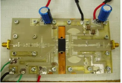
A power amplifier demonstration board was implemented by using the Taconic RF35 characterized previously and the RFIC MRF7IC3825 field effect transistor. In order to design the input and output matching networks, we used wideband topologies implemented with the combination of lumped and distributed components.
methods based only on narrow band topologies with lumped components [7]. The objective of that design is to provide to the transistor the impedances obtained by the source pull and load pull measurements, which were selected to provide the best trade-off between power, linearity and efficiency [11]. For measuring the device and its impedances, micro-strip probes were implemented in the same substrate, RF35, as it is shown in Fig. 6, with SMA connectors.
Fig. 6. Implemented RF probes in RF35 substrate.
[image:4.595.316.541.318.392.2]The matching technique mentioned above let us to use few components because the most of them were printed on the PCB [11]. Consequently, we got to minimize the insertion loss of the matching networks and increase the index of repeatability at the industrial production level. The DC feeders on the drain side were implemented based on the printed butterfly technique which allowed us to have around -30dB isolation from 3.2 until 3.9GHz. As it is depicted in Fig. 7, a symmetric feeder was also implemented in the drain side in order to improve the video bandwidth behavior, reducing intermodulation distortion at a minimum value [11].
Fig. 7. Photo of the implemented power amplifier. The RFIC is a courtesy donation from Freescale.
We polarized the device in order to see properly the P1dB compression point. By doing that, we got a power gain around 22.8dB. Furthermore, the gain flatness was 0.5dB approximately from 3.4 until 3.6GHz. Those results are shown in Table I. In terms of power, we verified that the output power was 29W in P1dB conditions [11]. The total efficiency was approximately 34%. By testing the amplifier in WIMAX conditions, we got nearly 23dB gain.
TABLEI.PERFORMANCEOFTHEAMPLIFIERUNDERP1DBAND WIMAXCONDITIONS
Once a final PCB was implemented with this methodology
[image:4.595.76.273.415.549.2]we proceed to perform a sanity check in order to guarantee the reliability of the final product. For P3dB power sweeps test, the repeatability of RF performance was verified. The ruggedness of the device was also verified through VSWR measurements by using a sliding short. In this last test we have seen oscillations in all the cases. We addressed the problem of oscillations with an RC network for stabilization on drain feeder. As it is indicated in the lower right hand-side in Fig. 7, the stabilization network consists in a 10 Ω resistor in series with a 33 pF capacitor. Repeating the previous test with the stabilization network, we verified once again the good RF performances and ruggedness. To evaluate the ruggedness over temperature, VSWR test was carried out for three different temperatures: 85, 25 and -30°C. No spurious in the frequency domain were observed in those conditions, except at 3.6GHz at Vds=32V; however, those conditions are outside the customer’s specification range as it is shown clearly in Fig. 8. This information is used for stablishing the limits of operation of the transistor in the datasheet.
Fig. 8. Sanity check for different biasing, frequencies and temperatures.
[image:4.595.318.561.473.610.2]Gain was also measured, with respect to temperature, given us a variation of -0.05 dB/°C, which is normal for this kind of devices. Results are shown in Figs. 9 – 10.
[image:4.595.317.547.638.833.2]Fig. 10. Delta Gain Vs. temperature.
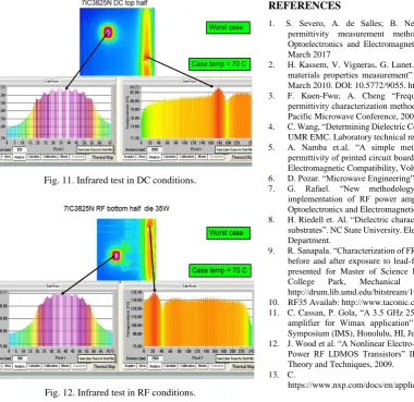
[image:5.595.58.439.364.733.2]In terms of power, the output power variation was -0.89W/°C. This excellent stability performance is due to the thermal tracking technique used in the RFIC [12] - [13]. This technique creates a feedback loop from drain to gate in order to stabilize the bias point with respect to gain variations due to the temperature. This procedure is very well known for BJTs, and it has demonstrated to be also valid for field effect transistors. Furthermore, infrared measurements over the PCB, with the transistor biased without package, showed 87°C for the die and 83°C for the output wires in DC. The transistor was decaped by using a hot plate at around 300°C. In RF conditions at 35W output power (8dB back-off) the wire temperature was around 180°C. Those results are shown in Figs. 12-13. For the infrared test it is possible to conclude that, in DC conditions, the distribution of temperature is nearly constant for the RFIC. For RF conditions, the distribution of temperature is slightly higher in the bottom side. For the output wires, the distribution of temperature in the bottom side is almost 20°C higher than in the top side. Those values correspond to a normal behavior of this technology under infrared test. It is important to mention that there were not reported medium term and long term memory effects in this RF LDMOS high power amplifier.
[image:5.595.211.541.375.814.2]Fig. 11. Infrared test in DC conditions.
Fig. 12. Infrared test in RF conditions.
Other power amplifiers were also implemented by using a similar method [7] but at lower frequencies, however; this is the first time in which thermal measurements were used to
evaluate the performance of a 3.5GHz amplifier implemented by using the one-port substrate characterization technique.
V. CONCLUSION AND FUTURE SCOPE In this paper it is shown the impact of the one-port substrate characterization process on the implementation of a 3.5GHz RF power amplifier. Firstly, it has been demonstrated that the effects of ℰr and tan δ over return loss are independent and allow the direct extraction of the substrates parameters using single port measurements. Secondly, we have shown that comparison with conventional techniques demonstrates the similar effects. Then, we have seen that by measuring the reflection coefficient at only one port at resonant frequencies, the proposed method is accurate and a low cost solution for environments in which VNAs are not available. Several simulators, such as ADS and AWR, were used to validate our method. Finally, a high frequency power amplifier, critically dependent on substrate characterization, was implemented by using the proposed technique. The electrical and thermal performances confirmed the validity of this novel approach. The next step will be the implementation of a Doherty amplifier in the GHz range in which substrate characterization is even more critical due to the use of two transistors in parallel topology.
REFERENCES
1. S. Severo, A. de Salles; B. Nervis, B. Zanini. “Non-resonant permittivity measurement methods”. Journal of Microwaves, Optoelectronics and Electromagnetic Applications, Vol. 16, No. 1, March 2017
2. H. Kassem, V. Vigneras, G. Lunet. “Characterization techniques for materials properties measurement” University of Bordeaux, France. March 2010. DOI: 10.5772/9055. https://www.researchgate.net 3. F. Kuen-Fwu; A. Cheng “Frequency domain propagation and
permittivity characterization method for printed circuit boards”; Asia Pacific Microwave Conference, 2009. APMC 2009.
4. C. Wang, “Determining Dielectric Constant and Loss tangent in FR-4”, UMR EMC. Laboratory technical report: TR00-1-041. March (2000). 5. A. Namba et.al. “A simple method for measuring the relative permittivity of printed circuit board materials” IEEE Transactions on Electromagnetic Compatibility, Volume: 43 Issue:4. Nov 2001. 6. D. Pozar. “Microwave Engineering”. 3rd Ed. John Wiley & Sons. 7. G. Rafael. “New methodology for modeling, design and
implementation of RF power amplifiers” Journal of Microwaves, Optoelectronics and Electromagnetic Applications, Sept 2017 8. H. Riedell et. Al. “Dielectric characterization of printed circuit board
substrates”. NC State University. Electrical and Computer Engineering Department.
9. R. Sanapala. “Characterization of FR-4 printed circuit board laminates before and after exposure to lead-free soldering conditions”. Thesis presented for Master of Science Degree. University of Maryland, College Park, Mechanical Engineering. August, 2008. http://drum.lib.umd.edu/bitstream/1903/8362/1/umi-umd-5671.pdf 10. RF35 Availab: http://www.taconic.co.kr/english/download/RF-35.pdf 11. C. Cassan, P. Gola, “A 3.5 GHz 25 W Silicon LDMOS RFIC power amplifier for Wimax application”. IEEE International Microwave Symposium (IMS), Honolulu, HI, June 3-5, 2007.
12. J. Wood et al. “A Nonlinear Electro-Thermal Scalable Model for High Power RF LDMOS Transistors” IEEE Transactions on Microwave Theory and Techniques, 2009.
13. C. Cassan.
https://www.nxp.com/docs/en/application-note/AN1987.pdf
AUTHORS PROFILE

![Fig. 5. Simulations (x) and measurements (o) of return loss for the FR-4 [11].](https://thumb-us.123doks.com/thumbv2/123dok_us/8199144.260272/3.595.57.282.147.322/fig-simulations-x-measurements-o-return-loss-fr.webp)