A Programmable Time Measurement Architecture for Embedded Memory
Characterization
1Matthew Collins, Bashir M. Al-Hashimi and Neil Ross
School of Electronics and Computer Science, University of Southampton,
Highfield, Southampton SO17 1BJ, UK
Email:
[email protected]
,
[email protected]
,
[email protected]
Abstract
This paper describes a programmable time measurement architecture that facilitates memory characterization. We have created a novel standalone time measurement architecture that can measure rise time, fall time, pulse width and propagation delay time measurements without the need of additional circuitry [1] or circuit duplication [2]. This is achieved by the use of Time-to-Digital Conversion (TDC) based on the dual-slope principle. The key feature of the proposed architecture is programmability through the use of a novel programmable input stage. Furthermore, a current steering Time-to-Voltage Converter (TVC) is used in order to improve the linearity and dynamic range as compared to recent designs. The proposed architecture has been designed using 0.18µm CMOS process and results from simulations using foundry models suggest it is possible to achieve a timing resolution of 103ps. The measurement core size is 110µm x 75µm.
1. Introduction
In modern SoC designs, embedded memory has become an important building block and has a great influence on the area and yield of a System-on-Chip (SoC) device. The ITRS’03 predicts that by the year 2016, ninety five percent of the total area of a SoC device will be occupied by memory [3]. With the continuous speed scaling, increase area and the increase in cost of automatic test equipment (ATE) characterization of embedded memory has become an important issue. Recently, techniques for characterising embedded memories have been proposed [1, 4]. The architectures proposed in [1] and [4] have targeted memory access time measurements and setup and hold times only. This limits the application of such
architectures where more time measurement parameters are needed to be obtained. We present a standalone timing measurement architecture that can be incorporated with embedded memory to obtain most timing measurement parameters without the need of additional circuitry or circuit duplication. Furthermore, linearity is a key issue in time measurement architectures, as it has an impact on resolution and dynamic range. This paper analyzes the performance of current Time-to-Voltage Converters (TVCs) and integrates a current steering Time-to-Voltage Converter (TVC) architecture that has improved linearity and dynamic range as compared to previous designs.
This paper is organised as follows. Section 2 introduces the principles of the proposed time measurement architecture for characterizing embedded memories. The features of the main circuit components are described here. Section 3 presents simulation results of the proposed architecture and finally in section 4 conclusions and future work are given.
2. Proposed Architecture
Various techniques for time measurement have been proposed [2, 5-8]. We have chosen the TDC method because of its simplicity and high resolution capability. Figure 1 depicts the proposed time measurement architecture. The circuit is composed of three parts, a programmable interface block, a time-to-voltage converter and a digital processing block to generate an N-bit digital output code. In order to configure the time measurement circuit, two pins: mode0 and mode1 are programmed. The modes of operation are shown in Table 1.
Table 1. Modes of operation Mode1 Mode0 Measurement
0 0 Rise Time
0 1 Fall Time
1 0 Pulse Width
1 1 Propagation Delay
1This work is supported in part by the EPSRC, U.K., under grant
Figure 1: Proposed timing measurement architecture block diagram
Figure 2: Programmable Interface Block
The programmable interface block (PIB) consists of seven dynamic switches, a rail-to-rail comparator and some control logic. Internal references VrefH, VrefM and VrefL are generated internally via a bandgap reference. As the current design is targeted for a 1.8V 0.18µm process the reference voltages are currently 1.62V, 0.9V and 180mV respectively. In order to facilitate a rise time measurement, switches sw<1> and sw<4>, as shown in Figure 2, are closed in order for the comparator to compare the input rising signal with the applied VrefL. As soon as the output of the comparator goes high, both switches sw<3> and sw<6> turn on and sw<1> and sw<4> turn off. This now allows the comparator to compare the input voltage with VrefH. When the input voltage crosses the VrefH reference voltage, the output of the comparator goes low. The output of the comparator passes through a switch that is opened by the high to low transition of the comparator output to form a single pulse that represents the time duration of the rising edge of the input voltage. This pulse is then converted into a voltage by the use of a Time-to-Voltage Converter (TVC) which is described in section 2.2. Finally, a digital processing block generates an N-bit digital output code. A fall time measurement is achieved in a
similar way but the references VrefH and VrefL are reversed. For pulse width measurements switches sw<0> and sw<4> are used first and then switches sw<3> and sw<5> to compared the Vin1 input with VrefM, and for propagation delay measurements switches sw<0> and sw<4> are used and then sw<2> and sw<5>, so that Vin1 and Vin2 can be compared with VrefM.
2.1 High Speed Comparators
The comparator is a very important part of any time measurement architecture. In order to achieve 10% and 90% rise and fall time measurements a comparator must have a wide input common mode range (CMR) [2]. A schematic of a rail-to-rail clocked comparator is shown in Figure 3 [9]. The transistor sizes are shown in Table 2. The input of the comparator consists of a rail-to-rail input stage that contains two complementary differential pairs in parallel. When one of the common-mode (CM) inputs is close to VDD, differential pair M1 and M2 is active. When the common-mode input is close to VSS, differential pair M3 and M4 is active.
[image:2.612.207.407.212.370.2]by a bias circuit; this is not shown for simplicity. The operation of the comparator is as follows. When Vlatch is low, the comparator is in a reset state and transistors M11 and M12 couple the drains of transistors M9 and M10 to VDD. Transistors M13 and M14 are off and there is no supply current flowing. When Vlatch is high, transistors M11 and M12 are open. The cross
[image:3.612.124.501.164.668.2]coupled regenerative inverters amplify the voltage difference and one of the output nodes is at VDD and the other is at VSS. Figure 4 shows the comparator simulation results. With a CM input voltage of 1.62V, a propagation delay (measured from the 50% of the clock signal to the 50% output low to high transition) of 200ps is achieved with a capacitive loading of 50fF.
[image:3.612.184.463.328.662.2]Figure 3: Rail-to-Rail Comparator
Table 2. Transistor sizes
Device Width (µm) Length (µm) M1 1.2 0.2 M2 1.2 0.2 M3 3.4 0.2 M4 3.4 0.2 M5 1.2 0.4 M6 3.4 0.4 M7 1.2 0.2 M8 1.2 0.2 M9 3.4 0.2 M10 3.4 0.2 M11 3.4 0.2 M12 3.4 0.2
Figure 4: Rail-to-Rail Comparator Simulations
Clock
Input
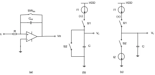
Figure 5: Current TVC implementations for embedded memory characterization
2.2 Time-to-Voltage Conversion
The TVC is based on the dual-slope technique of charging up a capacitor C, in a time interval T1 using a constant current source, Ich, and discharging it at a
slower time interval T2 using another constant current source Idis. This technique is widely used in time
measurement architectures [2, 4, 10]. The timing parameters can be calculated as follows. During the charging phase of the TVC, the voltage at the integration capacitor is given by:
1
T C I V ch
ch = ∗∆
∆ (1)
During the discharge phase the capacitor voltage is given by:
2
T C I Vdis = dis ∗∆
∆ (2)
Where
clk
T Count T = ∗
∆ 2 (3)
Equating ∆Vch = ∆Vdis gives
clk dis
ch Count T
C I T C I
∗ ∗ = ∆
∗ 1 (4)
Therefore
clk ch
dis Count T
I I
T = ∗ ∗
∆ 1 (5)
As can be seen in equation (5), the input measurement,
∆T1, is a function of the ratio of the discharging
current, Idis and the charging current, Ich. Therefore the
accuracy of the currents, Ich and Idis, has little effect on
the accuracy of the measurement and temperature effects can be minimised by current layout techniques of current mirrors. A number of circuits have been proposed to implement the TVC [1, 4, 10]. Figure 5 shows a simplified view of the current implementations. In this section we compare the performance of each circuit and propose an improved
architecture. Configuration 5(a) is based on an integrator, where the capacitor Cint is charged and
discharged by SWdis. Configuration 5(b) and 5(c) are
very similar in that when switch S1 is closed, they both use a constant current source, I1, to charge up the capacitor, C. The resulting voltage ramp is directly proportional to the time and the voltage across the capacitor, Vc, is given by equation (6).
t C I t
Vc()= 1∗ (6)
When switch S2 is closed and switch S1 is opened, the capacitor discharges. The difference is that Figure 5(c) uses a constant current I2 to slowly discharge the capacitor. Each of the configurations in Figure 5 has non-linearities which limit their dynamic range. Configuration 5(a) has non-linearity caused by the settling time of the opamp. Both configurations 5(b) and 5(c) have non-linearity in their voltage transfer curves (VTC) as shown in Figure 6.
Figure 6: VTC of configurations (b) and (c).
This non-linearity arises because when switch, S1, is open, the voltage at node (x) is at VDD, but when S1 closes, this voltage rapidly falls to zero. This requires charge redistribution in the transistors of the current source which leads to a transient current in excess of the steady-state current. In order to avoid this, the current from the current source maybe diverted through a second switch while S1 is open. Figure 7 shows such a circuit. This type of circuit is often used in PLLs [11]
Figure 7: Current Steering Time-to-Voltage Converter (TVC)
Figure 8: Simulations of TVC
but we have used it in our TVC to achieve better linearity and dynamic range. It uses a complementary input to steer the charging current through transistor M3 when M4 is open. Thus holding node (x) stable and preventing the gate of M9 being pulled down due to charge flowing through the gate-drain capacitance. A similar switching scheme is used for the discharging current. Simulations of the current steering TVC and the commonly used configuration 5(b) are shown in Figure 8. As can be seen from the simulations the current steering TVC has better linearity and dynamic range compared to that of configuration 5(b).
3. Simulation Results
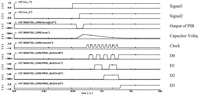
To verify the proposed time measurement architecture, the design was implemented using a 0.18µm CMOS process. The core architecture is 110µm x 75µm. The charging and discharging currents are Ich = 41.3µA and Idis = 8.5µA. Figure 9 shows the simulation results of the proposed architecture. Signal1 and Signal2 have a propagation delay time of 950ps. The capacitor voltage shows good linearity brought about by incorporating the current steering TVC which has improved linearity
and dynamic range compared to previous configurations. The digital output code D0-D3 generated by the digital processing block was 10012 = 910. Using equation (5), the measured value can be calculated.
clk ch
dis Count T
I I
T = ∗ ∗
∆ 1
ps
15 . 926 10
* 500 * 11 3 . 41
5 .
8 ∗ 12 =
= −
This gives a measured value of approximately 927ps. The percentage error can be calculated using the following equation.
% 100 _
_ _
%= − ∗
value actual
value actual value
measured Error
% 42 . 2 % 100 * 950
950 927
= −
=
ps ps ps
This gives an error of 2.42 percent. The main cause of this error is the programmable input block, where a delay is introduced by the propagation delay of the comparator and the input switches. Table 3 shows the results of the different measurements made using this
Configuration 5(b) Current Steering TVC
[image:5.612.207.403.257.405.2]Signal1
Signal2
Output of PIB
Capacitor Voltage
Clock
D0
D1
D2
[image:6.612.174.495.72.228.2]D3
Figure 9: 950ps propagation delay time measurement
Table 3. Results
Measurement Actual [ps] Count Measured [ps] Error [%]
Rise Time 960 9 927 3.44
Fall Time 960 9 927 3.44
Pulse Width 950 9 927 2.42
Propagation Delay 950 9 927 2.42
Propagation Delay 1000 9 927 7.3
Propagation Delay 1300 13 1338 2.92
self contained architecture. The clock frequency of the counter is set to 2 GHz. This gives a measurement timing resolution of 103ps
4. Conclusions and Future Work
In this paper, we have presented a novel standalone programmable time measurement architecture that facilitates memory characterization that is capable of measuring four timing parameters. Simulations using transistor models based on a 0.18µm CMOS process show that measurements are capable with a resolution of 103ps. It has been shown that it is possible to develop an architecture that is small and capable of measuring a number of timing parameters and have better linearity and dynamic range through the careful section of TVC and comparator. Although current compensation techniques show good results our future work will concentrate on the compensation of the measurement error caused by the input stage.
5. References
[1] M.-j. Hsiao,J.-R. Huang,T.-Y. Chang, "A Built-In Parametric Timing Measurement Unit," IEEE Design and Test of Computers, vol. 21, pp. 322-330, 2004.
[2] T. Xia,J.-C. Lo, "On-Chip Short-Time Interval Measurement for High-Speed Signal Timing Characteristics," 12th IEEE Asian Test Symposium (ATS'03), pp. 326-331,2003.
[3] "International Technology Roadmap for Semiconductors," http://public.itrs.net/Files/2003ITRS/Home2003.htm, 2003.
[4] S.-R. Lee,M.-J. Hsiao,T.-Y. Chang, "An Access Timing Measurement Unit of Embedded Memory," 11th IEEE Asian Test Symposium (ATS'02), pp. 104-109,2002.
[5] F. O. Mahony,C. P. Yue,M. A. Horowitz,S. S. Wong, "A 10-GHz global clock distribution using coupled standing wave oscillators," IEEE JSSC, vol. 38, pp. 1813-1820, Nov 2003.
[6] S. Tabatabaei,A. Ivanov, "Embedded timing analysis: A SoC infrastructure," IEEE Design and Test of Computers, vol. 19, no. 3, pp. 22-34, 2002.
[7] P. Chen,S.-I. Liu,J. Wu, "A CMOS Pulse-Shrinking Delay Element for Time Interval Measurement," IEEE Trans. on Circuits and Systems-II: Analog and Digital Signal Processing, vol. 47, No. 9, pp. 954-958, Sept 2000.
[8] C.-S. Hwang,P. Chen,H.-W. Tsao, "A High-Resolution and Fast-Conversion Time-to-Digital Converter," IEEE Inter. Symp. on Circuits and Systems (ISCAS'03), vol. 1, pp. 37 - I-40,2003.
[9] R. J. Baker, CMOS: Circuit Design, Layout, and Simulation, 2nd Edition: Wiley-IEEE Press, 2005.
[10] E. Raisanen-Ruotsalainen,T. Rahkonen,J. Kostamovaara, "Time Interval Measurements using Time-to-Voltage Conversion with Built-In Dual-Slope A/D Conversion," IEEE Inter. Symp. on Circuits and Systems (ISCAS'91), vol. 5, pp. 2573-2576,1991.