University of Southern Queensland
Faculty of Health, Engineering and Sciences
VAR Controller for STATCOM Solar Inverter
A dissertation submitted by Akshay Jaishil Sahay
In fulfillment of the requirements of
Courses ENG4111 and ENG4112 Research Project Towards the degree of
Bachelor of Electrical and Electronics Engineering
Abstract
In the past five years over 1.2 million PV installations were made in Australia which has had a detrimental effect on the overall power quality of the system. Utilities now provide a higher level of system harmonics as well as having to cope with unintentional DC current injection into the grid. At the same time, these PV installations have not helped the utilities at peak periods, or for localized loads such as starting of induction machines. Thus there is clearly a need for a more dynamic inverter system which can help improve system efficiency and maintain power quality standards.
In order to help improve the power quality of the grid, the existing STATCOM inverter would be adapted to monitor grid conditions with a smart energy meter and interfaced to a PLC to either bring voltage within limits or improve power factor to a desired level. The PLC will utilize both power factor information and voltage and current information from the smart energy meter to allocate an active power and a reactive power of either a capacitive or inductive reactive power in order to maintain power factor levels. Weak networks suffer from a range of problems depending on conditions. Typically when they are heavily loaded, they require additional capacitive reactive power to be injected into the grid. On SWER networks, due to the high X on R ratio they also require at peak times the injection of active power. When lightly loaded by comparison, they require the injection of reactive power in order to bring the voltage within limits due to the Ferranti Effect. In order to accommodate all of these functions, the power factor and the voltage conditions from the smart energy meter were read into the PLC where the decision was made as to what level of active, capacitive reactive or inductive reactive power was required to be injected into the grid. A set of SIMULINK models were developed to analyze a range of switching strategies in order to minimize injected harmonics and maximize STATCOM efficiency. The key outcome of this project was that the implementation of a PLC based system which provided active and reactive power support and was able to react to localized load changes rapidly. The broad application of this technology to existing PV systems will ultimately allow in system power quality and efficiency improvements throughout the state.
University of Southern Queensland
Faculty of Health, Engineering and Sciences
ENG4111/ENG4112 Research Project
Limitations of Use
The Council of the University of Southern Queensland, its Faculty of Health, Engineering & Sciences, and the staff of the University of Southern Queensland, do not accept any responsibility for the truth, accuracy or completeness of material contained within or associated with this dissertation.
Persons using all or any part of this material do so at their own risk, and not at the risk of the Council of the University of Southern Queensland, its Faculty of Health, Engineering & Sciences or the staff of the University of Southern Queensland.
Certification of Thesis
I certify that the experimental work, results, analyses, software and conclusions reported in this dissertation are entirely my own efforts, except where otherwise acknowledged. I also certify that the work is original and has not been previously submitted for any other award, except where otherwise acknowledged.
Akshay Jaishil Sahay 0061020131
Signed: _____________________ Dated: _____________________
Acknowledgment
I would like to take this opportunity to express my sincerest and deepest gratitude to the following people, without whom the completion of this research project would not have been possible.
1. My Supervisor, Dr. Leslie Bowtell for all his patience, support and the skillful and tactful guidance during the course of my research project.
2. The University of Southern Queensland Technical staff, in particular Mr. Graham Holmes, Mr. Brett Richards and Mr. Terry Byrne for their help in providing resources.
3. The staff at Futurlec Australia Pty Ltd, in particular their sales manager Alan, for all his help in providing the components and the prototyping of a printed circuit board (PCB) at very affordable prices and in a timely manner.
4. The staff at Bayarea Circuits for printing my PCB boards at student rates with a very fast turnaround time.
5. The staff at BEC Manufacturing Australia for their help with the production of my PCB boards at a very short notice.
6. Mr. Peter Taylor of PT Automations Gold Coast for his guidance and advice with regards to the Energy Meter section of my project.
7. I would also like to acknowledge my family, especially my parents and my sibling, for their continuous emotional, financial support and also for providing the continuous motivation through the course of this research project.
Contents
Abstract ...iii
Certification of Thesis ... v
Acknowledgment ... vi
List of Tables ... x
List of Figures ... xi
List of Symbols ...xiii
List of Acronyms ... xv
Chapter 1: INTRODUCTION ... 1
1.1 Background and Justification ... 1
1.2 Development of the Project Topic ... 3
1.3 Issues with the current design ... 3
1.4 Problem Statement ... 4
1.5 Project Aim ... 4
1.6 Project Objectives ... 4
1.7 Limitations ... 5
1.8 Thesis Overview ... 5
Chapter: 2 LITERATURE REVIEW ... 7
2.1 Overview ... 7
2.2 DC Offset Control ... 7
2.3 Output Current Harmonic Distortion ... 10
2.4 Smart Energy Meter: ... 14
2.5 PCB Design: ... 17
Chapter: 3 METHODOLOGY ... 20
3.1 Overview ... 20
3.2 Theory of the Design Process ... 21
3.2.2 Hypothesis of the Design Problem ... 21
3.2.3 Synthesis of the Design Problem ... 22
3.2.4 Validation of the Design ... 22
3.3 Needs Identification ... 23
3.4 Design Limitations ... 24
3.5 Design Constraints ... 24
3.6 Derivation of Design Criteria ... 25
3.6.1 Improved Data Acquisition ... 25
3.6.2 Power Factor Correction ... 25
3.6.3 Standardized PCB’s housing ... 26
3.6.4 Increased Safety ... 26
3.6.5 Ease and Cost of Manufacture ... 27
3.6.6 Easy to fault find and repair ... 27
3.7 Design Options ... 27
3.8 Ranking of Design Criteria ... 28
3.9 Proposed Method for VAR controller ... 29
3.10 Final Design Specification ... 32
3.11 Implementation ... 35
3.12 Testing Procedures ... 36
Chapter: 4 RESULTS AND DISCUSSION ... 39
4.1 Overview ... 39
4.2 Simulation Discussion ... 39
4.3 PCB Design and Implementation ... 46
4.4 STATCOM Inverter operations ... 50
4.5 VAR Controller ... 56
Chapter: 5 RECOMMENDATION AND FURTHER WORK... 58
Chapter: 6 CONCLUSION ... 59
6.2 VAR Controller ... 59
References ... 61
Appendix A ... 67
Appendix A.1: Overall Schematic of STATCOM Inverter ... 68
Appendix A.2: Bipolar Switching Circuit: ... 70
Appendix A.3: Unipolar Switching Circuit: ... 71
Appendix A.4: Multimodal Switching Circuit: ... 72
Appendix A.5: Mode Change Over Circuit: ... 73
Appendix A.6: Inverting Summer Circuit: ... 74
Appendix A.7: Zero Phase Shift Filter Circuit:... 75
Appendix B ... 76
B.1: Project Proposal: ... 77
B.2: Risk Assessment: ... 78
B.3: Project Timeline: ... 83
B.4: Resource Planning: ... 85
B.4.1: Materials, Equipment and Software: ... 85
Appendix C: ... 87
Appendix C1: Compliance Certificates: ... 88
Appendix C2: Test Certificates: ... 90
List of Tables
Table 3. 1: Design Ranking Table for STATCOM PCB design ... 28
Table 3. 2: Implementation Material Comparison ... 33
Table 3. 3: STATCOM PCB Specifications ... 34
Table B. 1: Risk Assessment Table ... 82
Table B. 2: Semester 1 Timeline ... 83
Table B. 3: Semester 2 Timeline ... 84
List of Figures
Figure 1. 1: Essential Components of a Grid-Connected STATCOM Inverter ... 2
Figure 1. 2: Breadboard version of STATCOM inverter ... 3
Figure 1. 3: Overview of Thesis ... 6
Figure 2. 1: - Physical Details for the UM72 and UM100 PCB Profiles (Source: Steven Engineering (Steven Engineering 2014) ... 18
Figure 2. 2: Actual Pictures of UM72 and UM100 PCB Profiles (Source: Steven Engineering (Steven Engineering 2014)). ... 18
Figure 3. 1: Flowchart of the methodology that was employed ... 23
Figure 3. 2: EDMI Modbus Translator designed by Smart Building Services (source: - Smart Building Services, 2012) ... 30
Figure 3. 3: EDMI Smart Meter connection to PLC ... 30
Figure 3. 4: Screenshot of EDMI Meter login (Courtesy of EDMI Ltd) ... 31
Figure 3. 5: EDMI Smart Energy Meter configuration for RS232 port (courtesy of EDMI PTY Ltd) ... 32
Figure 3. 6: Photo of overall setup ... 37
Figure 4. 1: Bipolar Switching with Ripple Filter Simulink Model ... 40
Figure 4. 2: Simulink model results of the Bipolar switching output ... 41
Figure 4. 3: Unipolar Switching with Ripple Filter Simulink Model ... 42
Figure 4. 4: Simulink Results for the Unipolar Switching Operations ... 43
Figure 4. 5: Multimodal Inverter with Delay Simulink Model ... 44
Figure 4. 6: Multimodal STATCOM Inverter Waveform... 45
Figure 4. 7: PCB 1 DIP Trace Circuit design ... 46
Figure 4. 8: PCB 2 DIP Trace Circuit design ... 47
Figure 4. 9: PCB 3 DIP Trace Circuit design ... 48
Figure 4. 10: Photo of Board one assembled ... 49
Figure 4. 11: Photo of Board two assembled ... 49
Figure 4. 13: Photo of Complete STATCOM inverter (fully assembled) on UM100 PCB
profile ... 50
Figure 4. 14: Block diagram of STATCOM inverter operations (Source: - Bowtell PHD Thesis (Bowtell 2010)) ... 51
Figure 4. 15: Photo with identification of components ... 52
Figure 4. 16: Overall STATCOM inverter setup ... 53
Figure 4. 17: Experimental Bipolar Switching Waveform ... 53
Figure 4. 18: Experimental unipolar switching waveform ... 54
Figure 4. 19: Experimental results for multimodal switching ... 55
Figure 4. 20: Thermal Test Results for the STATCOM inverter ... 56
Figure 4. 21: VAR controller hardware setup ... 57
Figure A. 1: STATCOM Schematic ... 68
Figure A. 2: Bipolar Switching Circuit Schematic ... 70
Figure A. 3: Unipolar Switching Schematic ... 71
Figure A. 4: Multimodal Switching Schematic ... 72
Figure A. 5: Mode Change Over Schematic ... 73
Figure A. 6: Schematic of Inverting Summer Circuit ... 74
Figure A. 7: Zero Phase Shift Filter Schematic ... 75
Figure B. 1: Project Specification ... 77
Figure C. 1: Compliance certificate Board 2 from Bayarea Circuits ... 88
Figure C. 2 Compliance Certificate for Board 3 by Bayarea Circuits ... 89
Figure C. 3: Bare board Test Certificate for Board 1 from Bayarea Circuits ... 90
Figure C. 4: Test Certificates for Bare Board testing of Board 3 from Bayarea Circuits ... 91
Figure C. 5: BEC Manufacturing Agreement page 1 ... 92
List of Symbols
DA- Inverter H-Bridge freewheeling diode DA+ Inverter H-Bridge freewheeling diode DB- Inverter H-Bridge freewheeling diode DB+ Inverter H-Bridge freewheeling diode ic DC offset correction current
icomp component of irefto compensate for switching delay ii inverter output current
io inherent DC offset current of the inverter output ip output current from PV panels
ipr active power component of current reference iqr reactive power component of current reference iref current reference to hysteretic current controller is Mains current
kc DC bus voltage sensor constant
ke proportional gain of analogue PI controller kh Hall effect current sensor constant
km coupling factor of 1:1 inductor pair kp Hall effect current sensor on DC side
kzvz =kd1 or kd2 = constant integration rate of the integral element of the digital DC offset PI controller
TB- Inverter H-Bridge IGBT TB+ Inverter H-Bridge IGBT
Tbi Mixed-mode current controller bipolar operation time tdf switching delay on current fall
tdr switching delay on current rise v Inverter output voltage
v1 output of first stage of dual stage RC DC offset sensor vc PV array bus voltage
vf input voltage across dual stage RC DC offset sensor vi integrator output voltage in analogue PI controller vL AC component of vf
vm digitally filtered PV array bus voltage for MPPT vo output voltage of dual stage RC DC offset sensor vref reference DC bus voltage
vs Mains (grid) supply AC voltage
vz output voltage of digital filter in digital DC offset controller
τd time constant of first order digital filter used in the digital DC offset sensor τf time constant of each nominally identical stage of the dual RC DC offset sensor τi analogue PI controller integration time constant
List of Acronyms
AC Alternating Current
DC Direct Current
EMC Electromagnetic Compatibility FFT Fast Fourier Transform
Hz Hertz
IGBT Insulated Gate Bipolar Transistor MPPT Maximum Power Point Tracking PLC Programmable Logic Controller
PV Photo-Voltaic
PWM Pulse Width Modulation RFI Radio Frequency Interference
RLLC DC offset sensor based on 1:1 coupled inductor SCADA Supervisory control and data acquisition STATCOM Static Synchronous Compensator
THD Total Harmonic Distortion UPS Uninterruptable Power Supply VAR Reactive Power
1
Chapter 1:
INTRODUCTION
1.1
Background and Justification
Due to the continuous increase in demand for electrical energy worldwide and the rapid depletion of fossil fuels, the need for efficient renewable energy sources has become paramount (Suganthi & Samuel 2012). Generation of electrical energy using photovoltaic (PV) and windmill systems in conjunction with static synchronous compensator (STATCOM) inverter is increasing rapidly worldwide. The generation of electricity using photovoltaic (PV) and windmill system in conjunction with static synchronous compensator inverters form Microgrids. It also gives the energy providing utilities the flexibility of sharing the electrical load between various Microgrids to help improve the power quality on the main electrical grid (Fathi & Hassan 2013).
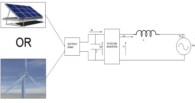
Figure 1.1 shows the most common configurations used with STATCOM inverters. However, the inverters are not limited to this configuration and can either be connected directly to the generation source or through the use of battery banks. A grid connected photovoltaic (PV) system usually has a battery bank connected to the STATCOM inverter. The photovoltaic panels convert the light energy from the sun into direct current (DC) which is stored in the battery banks. A battery bank is used to store the electrical energy for when the PV panels are not generating the energy. Since the electrical grids can only accommodate alternating current (AC), the DC current from the battery banks has to be converted into AC, in order for it to be used to supply to the electrical network. The inverter works as a DC to AC converter where it converts the DC current from the battery banks into an AC current of 50Hz which is then injected into the electrical network.
to a STATCOM inverter which converts the DC back into alternating current of 50Hz and injects it into the electrical network (US Department of Energy 2014).
Figure 1. 1: Essential Components of a Grid-Connected STATCOM Inverter
The optimal quality of alternating current that could be injected into an electrical network would be a purely sinusoidal alternating current. However this is not possible with even the highest quality or the most expensive inverters available on the market due to electronic limitations. Electricity utility companies specify limits on the direct current (DC) of the inverter output and the lower and higher harmonic contents of the inverter. This helps limit the distortion of the alternating current (AC) in the electrical network and also prevents damage to the electrical network devices. Harmonic currents causes electrical network equipment to generate heat and hence minimizes the lifespan of these devices (Wodrich 2007). The lower level harmonics comprises of current frequencies between the standard 50Hz and the 1 KHz frequency range (Wodrich 2007), whereas the higher level harmonics comprise of switching frequencies from inside the inverter. The electromagnetic interference (EMI) caused by the rapid switching inside the inverter also has to be limited due to the effect they have on other electronic devices (Kaur, Kakar & Mandal 2011).
1.2
Development of the Project Topic
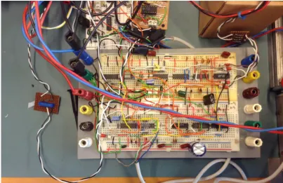
This research and implementation project was made available by Dr. Leslie Bowtell, lecturer for Electrical and Power Engineering at the University of Southern Queensland. Dr. Bowtell had initially started the research and implementation of this project during his PHD course and was able to implement an efficient bread board version of a four quadrant static synchronous compensator (STATCOM) inverter. During his PHD, Dr. Bowtell was constrained by time and was unable to implement a power factor correction unit and was unable to convert the inverter into a printed circuit board (PCB) form. The current bread board version of the STATCOM was lab tested and was found to be working as required, but without any power factor correction. It is because of this, the need for the project arose.
1.3
Issues with the current design
[image:17.595.123.527.486.747.2]The current version of the STATCOM inverter is breadboard based, therefore increasing the susceptibility of the electronic components to noise. There are also some safety concerns, due to exposure of high voltage live wires during the testing of the device. The device also does not have the ability to do power factor correction. Another problem associated with the STATCOM is that the wires used to connect the components to each other can be accidentally pulled out during the testing and probing process.
In order to significantly increase the safety for testing and probing purposes, and to avoid any of the wires connecting the components from being disconnected, it is essential that that the STATCOM inverter be converted into a printed circuit board (PCB). The device has to be redesigned, in order to include a power factor correction module so that the STATCOM inverter can be used to help improve the power quality in the grid.
1.4
Problem Statement
The current STATCOM inverter was tested in the laboratory and was found to be highly efficient with all four quadrants working properly. However, the current design posses’ safety risks due to high voltage wires being exposed. The STATCOM inverter also has capabilities to improve the power quality being provided which is not being utilized. This project will attempt to design a STATCOM inverter which eliminates the safety risks and will help improve the power quality by utilizing the power factor capabilities of the STATCOM inverter.
1.5
Project Aim
The aim of this project is to conduct research and implement a static synchronous compensator (STATCOM) inverter with a VAR controller which will enable power factor correction through the control of the reactive power of the inverter.
1.6 Project Objectives
The specific objectives of this project are:
1. Conduct a literature review in order to study and understand the current static synchronous compensator (STATCOM) inverter and their flaws. Using the literature review redesign a STATCOM inverter with greater efficiency and a VAR controller to improve the power factor using the reactive power of the inverter.
2. Using the information from the literature review design the printed circuit boards (PCB’s) using the UM 72 profile standard and the UM 100 profile standards. 3. Implement the printed circuit boards and do a laboratory setup of the hardware for
4. Interface the static synchronous compensator (STATCOM) inverter with a programmable logic controller (PLC) for control purposes and for power factor correction purposes.
5. Interface an energy meter with the programmable logic controller (PLC) to read the power factor from the main grid and to help in the power factor correction.
1.7
Limitations
This project will mainly focus on the redesign and the implementation of the four quadrant STATCOM inverter and the implementation of the VAR controller to enable power factor correction. In order for the device to be in compliance with the Australian Standards and International Organization Standards further work will need to be done. Once it is compliant with the Australian Standards, the device has some commercial value and would be beneficial in helping improve the power quality in the grids. Some of the work that has to be done for the device to be compliant with the standards include:
Design of a suitable equipment enclosure.
The design of a secure communications protocol
The two things listed above is out of the scope of this project and can form the basis of yet another Thesis for future Research students.
1.8
Thesis Overview
Chapter one of this dissertation introduces the reader to the rationale of the project and outlines the project aims and objectives.
The final results and an in depth discussions of the shortcomings are also provided in this chapter.
[image:20.595.183.473.167.748.2]Finally, chapter 5 gives a list of recommendations keeping in mind the results that were obtained from the testing process and also suggestions for the further development of the technology to make it more efficient and commercially viable.
Chapter: 2
LITERATURE REVIEW
2.1
Overview
This chapter contains a summary of the reviewed literature that was required for the successful implementation of this project. It reviews inverter DC injection control techniques, power quality assurance measures, energy meter interfacing and VAR control systems. The theoretical knowledge from the literature review has been used for the practical implementation of the STATCOM inverter with a VAR controller.
2.2
DC Offset Control
The output current of the inverter which is part of a grid connected PV system will ideally be purely AC. However, in practice this contains small amounts of DC unless certain measures are taken. If excessive DC injection occurs in AC mains, predicaments such as corrosion in underground equipment (Masoud & Ledwich 1999), transformer permeation, transformer magnetizing current distortion (Ahfock & Hewitt 2006) and malfunction of protective equipment (Bradley & Crabtree 2005) occurs. Consequently, guidelines and standards have been set up to govern DC injection (Salas et al. May 2006) (Salas et al. 2008). The AS4777.2 (Austrailian Standards Commission 2005) standard limits DC injection to 5mA or 0.5% of rated output whichever one is greater in Australia.
Sharma (Sharma 2005) have proposed the use of a feedback loop to eradicate the DC offset at the inverter output. The use of a voltage sensor at the inverter output with a differential amplifier and a low pass filter was proposed by Masoud (Masoud & Ledwich 1999) for the eradication of the DC offset. When using this method, any DC which may be detected at the output of the low pass filter is fed back to the controller which in turn operates the inverter in a way that reduces the DC offset. Although experimental results were not reported, a mathematical model was proposed for the control system and it is assumed that the inverter is voltage controlled.
An automatic adjustment scheme to vitiate the effect of the DC offset contributions from the Hall-effect current sensor in series with the DC input was proposed by Armstrong (Armstrong et al. 2006). In this scheme, an algorithm is used to ensure that the current measurement made during the freewheeling process is subtracted from all the measured current values. The major flaw in using Armstrong’s (Armstrong et al. 2006) technique is that it is limited to unipolar switched inverters, since the controls of the unipolar switched inverters enables easy measurement of the freewheeling intervals. Using large electrolytic capacitors in series to block any DC component in the current was proposed by Blewitt (Blewitt et al. 2010). When using this method, an additional fast control loop and a slower capacitor offset voltage control loop is required. Blewitt’s (Blewitt et al. 2010) results indicate that a maximum of 5mA of DC is injected into the grid. The use of a sensor at the output of the inverter to detect DC voltage offset and a DSP to affect control was proposed by Buticchi (Buticchi et al. 2009). The flaws with Buticchi’s (Buticchi et al. 2009) technique was that there were additional losses and hence it did not meet the requirements of the Australian Standards AS4777.2 (Austrailian Standards Commission 2005).
capacitor of the RC branch, allowing it to be fed back into the controller and hence adjusts the inverter current reference so that the DC offset is eliminated. For the method stated by Sharma, no quantitative experimental results were presented but a statement was made that the DC offset controller was found to be operating correctly (Sharma 2005). This method was then later validated by a mathematical model presented by Ahfock and Bowtell with quantitative experimental results (Ahfock & Bowtell 2006). The mathematical model that was presented by Ahfock and Bowtell was experimentally validated with results indicating that the 1:1 transformer is only effective if the primary winding time constant is sufficiently low, meaning that a relatively large core with low winding resistance is required (Ahfock & Bowtell 2006). This also indicates that the DC offset sensor is relatively large and expensive.
For the purpose of this project, a simple two stage RC filter will be used as the DC offset sensor. The DC sensor in this case would be connected across the ripple filter inductor at the output of the inverter bridge as proposed by Bowtell (Bowtell & Ahfock 2010) instead of it being connected across the AC supply terminal as proposed by Masoud (Masoud & Ledwich 1999) and Sharma (Sharma 2005). The advantage of connecting the DC sensor across the inverter bridge as opposed to connecting it across the AC supply terminal is that the offset sensor may sense offset currents which may not be related to the inverter at all and maybe from other sources when it is connected to the AC supply terminal, whereas when it is connected at the inverter bridge, it is only the inverter offset that is being sensed. The design of the DC offset controller that is being investigates the interaction between the DC offset control loop and the other control loops within the system similar to what was proposed by Bowtell (Bowtell & Ahfock 2010).
The three control loops that will be used in this project are:
The Current Control Loop
The DC Bus Voltage Control Loop
The Maximum Power Tracking Loop
control loops in detail. The current loop and the DC bus voltage loop operate independently to each other. The controllers are designed independent to each other so that the voltage controller can provide the reference signal that is required by the current controller. The independent design of the control loops enable the current loop to operate faster than the outer voltage loop which optimizes the performance of the inverter. During the designing of the voltage loop, it will be assumed that the current loop is a pure gain, whereas during the designing of the current loop, it will be assumed that the reference current has no influence on the controlled current in any way. For the purpose of this research project, the voltage control loop and the current control loop will be designed separate to each other as that is the industrial standard.
Another aspect of this project is the maximum power tracker. The maximum power tracker is an extremum seeking loop and hence does not require reference inputs like other loops.
Varjasi (Varjasi, Balogh & Halasz 2006), Gonzalez (Gonzalez et al. 2006) and many other researchers have considered the use of single stage conversion systems. This system will also be used for the purpose of this project. In the single stage conversion system, the voltage reference for the voltage control loop is provided by the maximum power tracker. Once set, the voltage reference is not immediately influenced by the other control loops. During operation, the maximum power tracker sets the reference voltage to a new value and then it waits for the voltage controller to change the DC bus voltage to the new value before it runs again. Hence, the assumption is made that the voltage control loop does not have any influence on the reference voltage.
During the course of this research, it was found that very little work had been published in peer reviewed journals with regards to the controlling of the DC offset current at the output of a grid-connected PV system. It was also found that very little work again was done in relation to the DC offset control loop and its interactions between the other control loops in the system. As part of this project, an independent DC offset control loop will be used under the assumption that the loop does not have any operational effects on the other loops in the system and vice versa.
2.3
Output Current Harmonic Distortion
typically in the 3rd, 5th, or 7th harmonic realms. This causes disturbance to the grid since that most power system devices are designed for 50 Hz. Therefore frequencies in the 150, 350 and 750 range causes significant increases in losses such as eddy current losses in physical hardware. High frequency harmonics such as the ripple frequency causes disturbances in the megahertz region, typically from a few kilohertz to megahertz region which can cause issues with Wi-Fi and other communication systems.
Due to the inverter continuously switching, it may cause the stray capacitances to charge and discharge very quickly. This may cause the frequency spectra of the stray capacitance to operate in the megahertz region and can potentially be a major source of electromagnetic interference (EMI). During the course of this research project, the effects of low frequency harmonics, ripple frequency harmonics and electromagnetic inference will be considered. The inverter which is being designed and implemented as part of this research project has to comply with the AS4777.2 (Austrailian Standards Commission 2005) standards, as this the standard for all the inverters that are being used in Australia. As per the standard (Austrailian Standards Commission 2005), all inverters are only allowed to have a maximum harmonic distortion of less than 5% for harmonics up to the 50th in the injected current for a grid connected PV system. Researchers such as
Kirawanich (Kirawanich & O'Connell 2000), Vasanasong (Vasanasong & Spooner 2000), Calais (Calais et al. 2002) and Spooner (Spooner 2001) have looked into the effects of harmonic injection in AC networks caused by the use of devices such as the inverter. All the measurements that were made by the researchers were based on commercially available grid connected inverters, the results of which indicated that the levels of low frequency harmonics were small. When these low frequency harmonics were compared against the requirements of the Australian Standard AS4777.2 (Austrailian Standards Commission 2005), it was found that the harmonics from those commercial inverters were still significant and were only barely meeting the requirements of the Australian Standard AS4777.2. It is because of these findings, the need for careful inspection of low frequency harmonics in grid connected inverters has arisen, with a common aim of either alleviating low frequency harmonics from the grid or to at least minimize the effects of the low frequency harmonics on the grid.
The research that has been done so far with regards to harmonics has mainly been focused around voltage controlled systems. Some of the possible causes of harmonic distortion in voltage controlled converters that were identified by Olivia (Olivia et al. 2005) are:
Dead-times
Device voltage drops
DC link voltage harmonics
A further explanation was provided by Mohan (Mohan, Undeland & Robbins 2005) on the relationship of dead-times and voltage harmonics. This explanation entails that the use of dead-times causes distortion to superimpose itself onto the voltage signal at the zero crossings. A simple mathematical model was derived by Kotsopoulos (Kotsopoulos, Heskes & Jansen 2002) to quantify the harmonic distortion levels at the zero crossings. Oliveira (Oliveira et al. 2003) suggests a technique that can be used with voltage controlled inverters to minimize the harmonic distortion at the zero crossing due to dead times. For current controlled inverters on the other hand, it was thought if the current reference signal was harmonic free, the current coming out of the inverter would also be free of low frequency harmonics. However, this was not the case, as Bowtell (Bowtell & Ahfock 2007) reported significant amounts of low frequency harmonics at the output of current controlled inverters. During this research, it was found that very vague information had been published in literature with regards to low frequency harmonic distortions in current controlled inverters. The few possible causes of low frequency harmonic distortion in current controlled inverters are identified as:
Distortion in the current reference signal as mentioned by Sakthivel (Sakthivel, Das & Kini 2003)
Distortion in the control signal generated by the voltage control circuit as reported by Sharma (Sharma & Ahfock 1992)
Switching Delays as published by Sharma (Sharma & Ahfock 2004) (Sharma & Ball 2009)
Dead-time as identified by (Olivia et al. 2005)
Quaicoe & Iqbal 2008) and Li (Li & Chung 2008) have suggested the use of a mixed mode inverter. The operation of the mixed mode inverter as proposed by the authors’ states that the unipolar switching should be used for most of the inverter’s cycle so as to reduce the switching loss and to use the bipolar switching near the zero-crossing to minimize the distortion around the zero-crossing area of the inverter.
A very small fraction of this research project will look at the possible causes of low frequency harmonics and zero crossing distortions in current controlled inverters. An investigation of these causes will highlight any short falls that maybe present. Understanding these shortfalls will provide data to further improve the device if needed and this will also reduce the distortion of the AC signal being fed back into the grid. Ripple frequency harmonics can easily be filtered out from the inverter using relatively small and low cost hardware. This however is not possible with regards to low frequency harmonics at the present time. Ripple frequency harmonics can easily be filtered using passive electrical components or a combination of passive components. Some of these passive components and combinations that could be used in filtering the ripple harmonics are:
Inductors (L)
A combination of inductor and capacitor (LC)
A inductor, capacitor, inductor filter (LCL filter)
not give proper consideration with regards to low frequency harmonics and ripple filter transients at the point of transition between unipolar and bipolar operations of the inverter. During the design process, careful consideration has to be given to the layout in order for the design to meet the necessary EMC requirements stated in the Australian Standards AS4777.2 (Austrailian Standards Commission 2005). It is a known fact that different circuit designs and configurations have different levels of EMI emissions. The EMI emission from the design and configurations is due to the stray capacitive currents that results from the very quick switching of the inverter. A brief theoretical explanation is given by Gonzalez (Gonzalez et al. 2006)with regards to charging and the discharging of stray capacitances between the source of the inverter (solar panel) and ground, however no experimental results were provided. A simulation based approach was used by Jiang (Jiang & Brown 2002) to report the EMC of inverters with different configurations. However, the configurations that were taken into account by Jiang are not being used for the purpose of this project. According to Gonzalez (Gonzalez et al. 2006) if the ripple filter was made up of two identical inductors, with one connected to the input of the inverter and the neutral, while the other is connected to the active terminal, the EMC performance of the bipolar operations is greatly improved in comparison to the unipolar operation EMC.
2.4
Smart Energy Meter:
Smart Energy Meters have started to play a very important role in modern energy distribution networks. Since the focus towards the generation and the usage of renewable energy has increased over the recent years, it has become essential for electricity suppliers and distributors to continuously monitor the service quality and often have to report the performance to governing authorities as mentioned by Capua (Capua et al. 2014). In order to acquire various information with regards to the service quality with minimal error, smart energy meters have to be used. Capua (Capua et al. 2014) breaks down the definition of service quality into three parts as defined below:
Reliability of supply
Voltage quality
According to Corbett (Corbett 2013), smart energy meters were designed to increase energy efficiency and to provide data to utility providers in real time. In this research project, data has to be provided in real time for the purpose of power factor correction. However, literature has not been provided for the proposed method of extracting the required information from the smart energy meter. Another major aspect is providing efficient energy using the method that is proposed in this project. According to Capodieci (Capodieci et al. 2011) people who produce and consume energy are called prosumers. Capodieci (Capodieci et al. 2011) also goes further into saying that these prosumers form a small part of the smart grid. A very comprehensive outlook into the design and the functioning of the smart energy meter is provided in Ali’s (Ali, Maroof & Hanif 2010) paper. An outstanding feature of the smart energy meter is that it has three ways of communicating information to remote control or monitor rooms. Two of these can be used simultaneously at any one time. These three ways of communication as highlighted by Ali (Ali, Maroof & Hanif 2010) are:
1. Localized digital display on which real time data is presented
2. Power Line Carrier Communication (PLCC) where the data is transmitted in real time to control/monitor rooms
3. Global System of Mobile (GSM) where the mobile networks are used to transmit the data in real time to control/monitor rooms.
PLCC is deemed as the most preferable medium of transmitting data from the smart energy meter in real time to remote control/monitor rooms. This is due to the fact that PLCC uses the same power transmission cables as its communication channel which in turn makes it immune to the effects of the surrounding environment. As per Ali’s (Ali, Maroof & Hanif 2010) paper, the information signal which is usually several kilo hertz from the smart energy meters is superimposed onto the power line which is usually operating on the 50 – 60 Hz range. This then eliminates the need for a separate channel which in turn eliminates the need for a separate transmission protocol.
not entirely true, due to the fact that there is always a delay associated with the use of text messaging. The data transmission is also subject to the network congestion as at times the messages are delayed by several minutes if the GSM networks are overly congested as explained in Verma’s paper (Verma, Sharma & Mishra 2012).
The use of these smart energy meters provides energy distributors more control over their network and also helps automate the switching process for when new users want to use their services. The smart energy meters contain a high voltage and high current relay inside them which allows the utility operators to switch on or off an energy service remotely. This eliminates the need for physical interaction when new services are to be connected to the network and hence reduces the cost and it also allows the utility operators to be more efficient as the service can be switched on instantly as described by Ali (Ali, Maroof & Hanif 2010).
Another very unique feature of the smart energy meter is its unique Anti-power theft system that it has incorporated in its design. This feature works on the basis that the digital meter inside the smart energy meter continuously monitors the amount of power used by a customer and it also has a feedback monitor which compares the amount of power used previously and the most recent consumption, alerting the utility providers of any discrepancies that is sensed as mentioned by Ali (Ali, Maroof & Hanif 2010). This feature allows the utility providers to investigate the possible theft of energy from their networks which in turn reduces their losses.
The functionality of the smart energy meter in the event of a power failure is also questioned by Ali (Ali, Maroof & Hanif 2010) and has been reported that the smart energy meters have a backup battery system installed in order to deal with a situation as such. Ali (Ali, Maroof & Hanif 2010) also further goes into the details of stating that the smart energy meters contain an EEPROM chip on which processed data is stored in the event of a communication failure between the smart energy meter and the utility control/monitor room. The data is also stored on the EEPROM chip when the smart energy meter is operating in its power failure mode and using its backup battery system to support itself.
proposed plan “the smart house”. Benzi’s paper goes further to say that in the smart house system, the utility providers and other service providers will be able to collect data from the localized computer and this will in turn make the information more readily available to everyone.
However, for the purpose of this project, the zigabee protocol cannot be used as per the discussion with the manufacturer of the particular smart energy meter being used in this project. According to EDMI PTY LTD, the manufacturer of the EDMI MK7C ATLAS smart energy meter that is being used in this research project, information from registers inside the smart energy meter cannot be transmitted using the zigabee protocol due to limitations of the hardware.
The proposed method of extracting the power factor information from the EDMI MK7C ATLAS smart energy meter is using a Modbus translator which is available as an additional component to the smart energy meter by the manufacturer. Using the Modbus translator and the Modbus function on the PLC, the required information is extracted from the smart energy meter for the processing and the comparison that is required. All the risks and flaws as identified by Ali (Ali, Maroof & Hanif 2010), Capodieci (Capodieci et al. 2011) and Capua (Capua et al. 2014) have been mitigated during the implementation using the methods that were proposed by them.
2.5
PCB Design:
1. UM72 Profile sizes:
72mm x 100mm
72mm x 200mm 2. UM100 Profile Sizes:
100mm x 72mm
100mm x 100mm
100mm x 120mm
100mm x 200mm
Figure 2. 1: - Physical Details for the UM72 and UM100 PCB Profiles (Source: Steven Engineering (Steven Engineering 2014)
[image:32.595.125.543.54.429.2]The sample schematic layout for the UM72 and UM100 profiles are shown in the above picture. It is essential that all three PCB boards that are required for the STATCOM inverter to function properly sit in the UM100 profile as it is more flexible with regards to length and because the UM72 profile was not available for use for this project.
Chapter: 3
METHODOLOGY
3.1
Overview
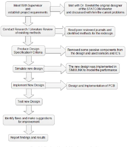
This chapter is based on the methodology that was employed to design, simulate and implement the four quadrant STATCOM inverter with a VAR controller which enabled power factor correction capabilities for in localized use and also when connected with the grid. The design of the PCB for the STATCOM was done using CAD software. The design was also simulated using SIMULINK so that theoretical waveforms were available for the purpose of comparing the actual waveforms from the STATCOM with. The chapter will also further explain the analysis that was used for the establishment of the design criteria, the design constraints that were used and the process used for the implementation of the designs. The first step involved meeting with Dr. Bowtell the original designer of the STATCOM inverter schematics that were modified for this project and discussed with him the original short falls of the first design. This meeting also set the boundaries and gave a clear definition of as to what was expected in this project and also set the limitations for the project. The discussions in this meeting led to the collection of information which were used in the redesign process.
The initial design of the STATCOM inverter that was made by Dr. Bowtell was of a current controlled mixed mode inverter which had both unipolar and bipolar operations, the advantages of which is detailed in Chapter 2 above. The initial design of the STATCOM inverter had various flaws which had to be rectified in order for it to operate more efficiently. During the discussion with Dr. Bowtell, some passive elements of the design were identified which were to be replaced by sensors and other active components. The new design of the STATCOM inverter was to include a VAR controller which would enable power factor correction for a localized household and will also have capabilities of correcting power factor in the power networks if allowed by the network operator. This then became the aim of the design process.
3.2
Theory of the Design Process
The definition of research according to Bock (Bock 2001) is the acquisition of new knowledge and the development of new processes using the acquired knowledge to create new inventions or to optimize current processes for the betterment of people. The development process will be used as part of this research project as the knowledge acquired from the literature reviews will be applied to optimize a current system and will also give rise to a new invention. The four parts of the scientific process as defined by Bock (Bock 2001) are:
Analysis
Hypothesis
Synthesis
Validation
The four parts as stated above will be used as part of this Research project.
3.2.1 Analysis of the Design Process
The analysis of the problem identifies the current flaws in the design and sets the objectives that are to be achieved at the conclusion of the research project. The objectives of this research project was explained in great detail in Chapter 1 so that the readers could understand what was tried to be achieved in this project. However, the objective in a nutshell is to redesign a four quadrant STATCOM inverter to remove some passive components in order to make the inverter more accurate and to implement a VAR controller to help correct the power factor in localized loads and also in the Grid if permitted by legislations and the network operator.
3.2.2 Hypothesis of the Design Problem
The VAR controller is going to be implemented the PLC as a logic algorithm for this project.
3.2.3 Synthesis of the Design Problem
Design problem synthesis includes designing the solution, implementing the solution, conducting experiments on the solutions that were implementing and collating and analyzing the results that were obtained. Since this research project involves a redesign component and also an implementation component, the redesigned STATCOM inverter will first be implemented and tested before the VAR controller is implemented with the device. This will ensure that the device functions the way it should. The redesigned inverter was simulated in SIMULINK before it was actually implemented in hardware. The simulations provided a theoretical comparison for the inverter and it also provided a certainty that when implemented the device is going to behave in a manner similar to what the simulations had shown.
3.2.4 Validation of the Design
Design validation involves computing the performance, drawing conclusions and preparing the required documentation. It also involves soliciting peer review from experts in the field. Once simulated, the STATCOM inverter was implemented onto PCB’s which was then lab tested. Only some of the performance indicators were looked at during the lab testing stage due to others being outside the scope of this research project and also due to time restrictions. Some examples of other performance indicators are:
Electromagnetic Compatibility (EMC) of the design
Electromagnetic Interference (EMI) in the design
Total Harmonic Distortion (THD) between the grid and the inverter
Communication between the inverter and the Grid operator
Figure 3. 1: Flowchart of the methodology that was employed
3.3
Needs Identification
3.4
Design Limitations
The design limitations for this project were identified as:
STATCOM equipment housing design is not part of this project
An existing S7200 version PLC was used for the purpose of bus voltage control
Power quality data i.e. power factor etc. is to be gathered by the EDMI energy meter.
3.5
Design Constraints
The following design constraints were identified for the design of the four quadrant STATCOM inverter and the VAR controller:
The PCB’s should fit a UM100 profile which restricts the size of the PCB’s to: 1. 100mm x 72mm (double layer)
2. 100mm x 72mm (single layer) 3. 100mm x 120mm (double layer)
The PCB’s design should no more than two layers.
The PCB’s design should minimize electromagnetic interference and switching noise, hence the track widths were increased from 0.1mm (standard track size) to 1.1mm which was the physical clearance limitation.
The pads for the components on the PCB’s were also made relatively thick. The pad sizes were increased from 1mm (standard pad diameter) to 1.5mm (This was again the maximum pad diameter before the pins on the IC’s short circuited themselves).
The PCB’s should interconnect between all the boards and other components such as gate drives and PLC relatively easily.
The STATCOM Inverter PCB’s should be insulated to handle 1000V minimum insulation requirements.
3.6
Derivation of Design Criteria
The design criteria were developed in accordance to the project specifications listed and agreed upon at the start of the project. An important aspect in the continued development of the design criteria was the recent technological developments identified in the Literature review.
3.6.1 Improved Data Acquisition
The increased accuracy in the data which is being obtained from the STATCOM inverter is essential for it to function efficiently. The STATCOM inverter relies on the voltage and the current information that it is supposed to obtain from the grid and also from the PV and battery bank side which is computed in the PLC. The VAR controller also needs to obtain accurate data in real time for the purpose of power factor correction. To increase the accuracy of the data being obtained by the PLC of the STATCOM, some passive and active components of the STATCOM inverter were changed from the original design. The new design of the STATCOM inverter included the use of modern hall-effect voltage and current transducers and also the use of a Smart Energy Meter for the purpose of more accurate data which was acquired by the PLC being used.
3.6.2 Power Factor Correction
method can also be used to improve the power factor in the grid but this is subject to legislative review and agreement between the utilities and the consumers.
3.6.3 Standardized PCB’s housing
A very important aspect of this research project was to make the design of the PCB’s as such that it will conform to a standard housing. The choice of housing for this project was chosen to be the UM100 PCB profile. The UM100 PCB profile was chosen as the standard equipment housing for this project because the size of the current controller for the inverter could only be reduced to 100mm x 120mm, which would have only fit the profile that can accommodate a PCB width of 100mm and in this case the UM100 PCB profile was large enough to accommodate it. The other two PCB’s that were part of the inverter were designed to the UM72 PCB profile specification and since their length was 100mm, they easily fit the UM100 PCB profile. Since all three PCB’s were designed as such that they could fit onto the UM100 PCB profile, it was decided that the UM100 PCB profile will be used for the housing since it reduced the need for the use of two different profile sizes and would allow the three PCB’s to be stacked on top of each other if the need arose, therefore standardizing the PCB housing for this project.
3.6.4 Increased Safety
Taking all this into consideration, the new design and implementation is much safer and user friendly then the old one.
3.6.5 Ease and Cost of Manufacture
Since this project has some commercial value in the future, the ease of manufacture and also the cost of manufacture has to be taken into account. Due to this redesign being only a prototype, it is understandable that the cost associated with it will be significantly higher than that when it is being manufactured on a large commercial scale. The components and IC’s that were used for the implementation are relatively cheap and are readily available on the market. Due to the IC’s being readily available, the cost of maintenance in the event that an IC malfunctions is significantly low. Currently the process of manufacture is manual but in commercial production it may be automated therefore removing most of the labor cost associated with it and hence reducing the cost.
3.6.6 Easy to fault find and repair
Fault finding is a very important aspect when trying to repair a circuit. The way a PCB is structured and the number of layers it has on it impedes on the fault finding process. To make the fault finding and repair process easier, all the PCBs had their component footprints and their values printed on the top layer of it. Fault finding and repair was taken into consideration during the designing of the PCB’s and hence all the boards were restricted to a maximum of two layers. With only two layers, it was easy to trace exactly where each of the tracks originated and where they ended.
3.7
Design Options
After looking at the project specification that was agreed upon, and thoroughly reviewing the literature, the following PCB designs were considered:
A = 1 x multilayered PCB housing the complete inverter measuring 72mm x 100mm
B = 1 x double layer PCB housing the complete inverter measuring 100mm x 200mm
C = 2 x double layer PCB board housing the complete inverter
measuring 100mm x 120mm each
power supplies and power tracking circuits measuring 72mm x 100mm and 1 x single layer PCB housing high voltage sensors and transducers. These four designs will be ranked against the design criteria that were derived above.
3.8
Ranking of Design Criteria
The ranking values for the design criteria was determined by the amount of impact each of the design criteria had on each of the design options. For the purpose of this project, a number scoring system was decided. The scoring system will work as follows:
10 points = high impact on design criteria
5 points = medium impact on design criteria
1 point = low impact on design criteria
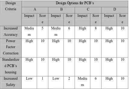
[image:42.595.114.541.482.778.2]Once all the design options are scored according to the design criteria, the scores are tallied and converted into a percentage. The design which has the highest percentage score, is dimmed the best option and is used in the implementation phase. The design options of A to D is carried forward from the previous section.
Table 3. 1: Design Ranking Table for STATCOM PCB design
Design Criteria
Design Options for PCB’s
A B C D
Impact Scor e
Impact Scor e
Impact Scor e
Impact Scor e Increased
Accuracy
Mediu m
5 Mediu
m
6 High 8 High 10
Power Factor Correction
High 10 High 10 High 10 High 10
Standardize d PCB’s
housing
High 10 High 10 High 10 High 10
Increased Safety
Low 1 Low 2 Mediu
m
Ease and Cost of Manufacture
Low 1 Low 1 Mediu
m
6 Mediu
m
6.5
Easy to fault find and
repair
Low 2 Low 2 Mediu
m
7 High 10
Total Score 29/60 31/60 47/60 56.5/60
Percentage Score
48.33% 51.66% 78.33% 94.16%
From the above ranking table, it can be seen that option D which is described as having three different PCB’s for the various parts of the STATCOM inverter has the highest scoring percentage of 94.16%. Since option D satisfies all the design criteria with quite high scores and it has the highest scoring percentage, this will be used for the purpose of this project.
3.9
Proposed Method for VAR controller
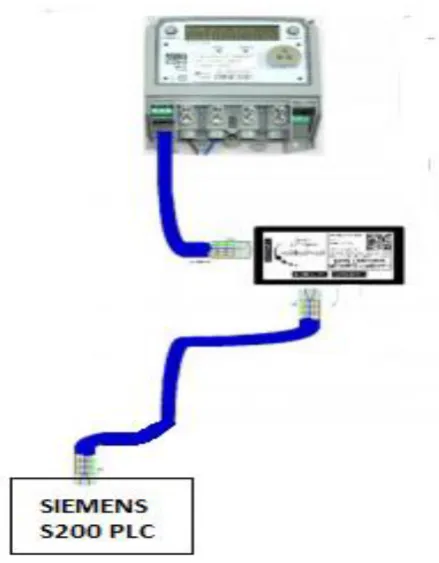
Figure 3. 2: EDMI Modbus Translator designed by Smart Building Services (source: - Smart Building Services, 2012)
Figure 3. 3: EDMI Smart Meter connection to PLC
[image:44.595.218.438.298.580.2]RS232 port has to be enabled for communication on the Smart Energy Meter. This has to be done using the software for the smart energy meter that was provided when the Smart Energy Meters were purchased. The standard means of communication for the Smart Energy Meters are the optical ports on the front of them. This optical port has to be used in order to get inside the meter settings and allow communication via the RS232 port. In order to turn on the RS232 port, it was necessary to log into the smart energy meter. The screenshot of how to logon to smart energy meter by adjusting the security settings is shown below and was provided by EDMI PTY Ltd.
Figure 3. 4: Screenshot of EDMI Meter login (Courtesy of EDMI Ltd)
Figure 3. 5: EDMI Smart Energy Meter configuration for RS232 port (courtesy of EDMI PTY Ltd)
Once all the parameters were setup correctly, and the communication port was enabled, the VAR controller algorithm was implemented. Further details about the VAR controller is discussed in the results section.
3.10 Final Design Specification
Table 3. 2: Implementation Material Comparison
Design Specifications and Physical factors
Old STATCOM Inverter New STATCOM Inverter
Material Type Standard
Breadboard
Vera Board
High Performance FR4 Substrate printed circuit boards
Connector types 2 pin pluggable block socket
3 pin pluggable block socket
2 pin MOLEX connector
3 pin MOLEX connector
4 pin MOLEX connector
10 pin MOLEX connector Potentiometer 25 turn PCB mount
with top adjuster
25 turn PCB mount with side adjuster
25 turn PCB mount with top adjuster
Capacitors Ceramic
Film
Ceramic
Film
Electrolytic
Resistors Film
Ceramic
Film
IC mounting Direct mounting
IC sockets
IC sockets
IC connection type DIP connections (through hole)
DIP connections
Table 3. 3: STATCOM PCB Specifications
Specification Board 1 Board 2 Board 3
Material High Performance FR4 substrate
High Performance FR4 substrate
High Performance FR4 substrate
Size 100mm x 120mm 72mm x 100mm 72mm x 100mm
Number of Layers 2 2 1
Track Width 1.1 mm 1.1 mm 1.1mm
Pad size 1.1mm 1.1 mm 1.1 mm
Minimum track clearance
0.5 mm 0.5 mm 0.5 mm
IC type 14 pin DIP
IC’s
16 pin DIP IC’s
8 pin DIP IC’s
14 pin DIP IC’s
5 pin DIP PCB voltage transducer
9 pin DIP PCB current transducer Connector types 10 pin
MOLEX
4 pin MOLEX
10 pin MOLEX
3 pin MOLEX
2 pin MOLEX
2 pin MOLEX
3 pin MOLEX Component connection type Through hole Through hole Through hole
Profile Standard UM100 UM72
UM100
UM72
UM100
3.11 Implementation
The first step in the implementation included updating the system schematic with the modifications that were made with regards to the removal of the passive components and the implementation of active components in its place. The schematic was drawn using Altium Designer Summer 09 version software and a copy of the schematic can be found in Appendix A.1 at the end of this thesis. Once the schematics were drawn, an initial prototyping on breadboards were done for the summer circuits and tested. This was done to verify that the summer circuit was performing as it was expected to. Once all the new active components that were replacing the passive components were tested on the breadboard and the results verified with the passive components, the schematic was then converted into a PCB design. Since the version of Altium Designer that was available did not contain all the libraries and the purchasing of the libraries would have been too expensive, an alternative PCB design software was used. The PCB design software that was used for this project was the freeware version of DIP Trace. The freeware version of DIP trace had all the necessary library files for the development of the printed circuit board designs for this project. Screenshots of the PCB designs are shown in section 4.3 of this thesis. Once the designs were completed, the PCB design files were converted into Gerber files so that the manufacturers could make the PCB’s. Upon completion of the conversion of the files, quotations were taken from local and international companies for the manufacture of these PCB’s. During the quotation process, it was found that local manufacture would have been too expensive for this project and hence international manufacturers were used. Boards 2 and 3 were manufactured in the United States and cost $30 dollars each to manufacture while Board 1 was manufactured in China for $40. The manufactures also provided a compliance certificate for the bare board testing that they had done. The compliance certificates can be found in Appendix C.
While the PCB’s were being manufactured overseas, the development of the SIMULINK models of the various switching types that are used in this STATCOM inverter were made. A SIMULINK model of the bipolar switching, unipolar switching and the multimodal switching were developed. The SIMULINK models provided a set of Theoretical results for comparison with when the STATCOM inverter was implemented in hardware.
manufactured, the PCB’s were then interfaced to a Siemens S7 – 200 PLC and the testing process was commenced. The testing process is described in detail in the following section. Upon the completion of the testing process and when the results that were obtained were dimmed satisfactory, an EDMI MK7C atlas smart energy meter was obtained and was interfaced to a PLC. Once the Energy Meter was successfully interfaced to the PLC, the power factor register from the smart energy meter was read via the MODBUS command. This power factor was then compared in the PLC. The PLC would have then triggered the Q control loop in order to enable the STATCOM inverter to push current into the grid to correct the power factor. In order to check if the power factor section is working, the STATCOM inverter first has to be commissioned and unfortunately due to time constraints the commissioning of the STATCOM inverter has been pushed onto a later date.
3.12 Testing Procedures
The following test procedures were used to obtain the results that are discussed in the following section of this report:
1. The laboratory power supply was configured to create a positive nine volts and negative nine volts with a floating ground. This was done to ensure that there were no ground loops in the setup and that everything had a single common ground connection.
Figure 3. 6: Photo of overall setup
Once the STATCOM inverter was connected to both the power supply and the PLC, a function generator which was producing a 50Hz sine wave was used as the reference current for the STATCOM inverter and a phase shifted 50Hz sine wave was used to as the input current for the STATCOM inverter. The results obtained are discussed in the following chapter.
3. Once the STATCOM inverter was tested and the results obtained were deemed satisfactory, the STATCOM inverter was interfaced with a SEMI TEACH DEVICE. This contained a heat sink, two large capacitors and isolated gate drives that would be used for the high voltage switching. Due to time constraints and the fact that the STATCOM inverter would have been required to be connected to the grid, this part of the testing was not done. This part of the testing has been left to the commissioning phase, where experienced University of Southern Queensland technicians who specialize in high voltage power would be available in order to supervise the high voltage testing.
the algorithm and getting the PLC to extract the register from the smart energy meter.
5. The first step of the VAR controller implementation involved the configuration of the hardware. The EDMI smart energy meter had to be connected to the SBS MODBUS translator in order to extract the power factor register from it. The MODBUS translator was then connected to a network switch which in turn was connected to a computer and a PLC.
Chapter: 4
RESULTS AND DISCUSSION
4.1
Overview
This chapter looks at the results of research carried out in the project and compares theoretical results from SIMULINK models for various switching topologies, which are unipolar, bipolar and multimodal. It also discusses aspects of the PCB design and delivered product.
4.2
Simulation Discussion
For the purpose of acquiring theoretical results, SIMULINK models were made. The SIMULINK models were made for:
1. Bipolar Switching 2. Unipolar Switching 3. Multimodal Switching
A standard version of MATLAB was used for the creation of this SIMULINK models and therefore all the blocks are just basic mathematical functions. These functions work together simultaneously to produce the waveforms that are expected from the actual STATCOM inverter once it is implemented. These theoretical results form the basis of the resul