Regular Article
Devitri
fi
cation of ultrafast laser plasma produced metastable glass layer
Jayakrishnan Chandrappan
a,⁎
, Vishal Khetan
b, Michael Ward
c, Matthew Murray
a, Gin Jose
a aSchool of chemical and process engineering, University of Leeds, LS2 9JT, UK
b
School of mechanical engineering, University of Leeds, LS2 9JT, UK
cLeeds electron microscopy and spectroscopy centre, University of Leeds, LS2 9JT, UK
a b s t r a c t
a r t i c l e i n f o
Article history:
Received 21 October 2016 Accepted 20 December 2016 Available online xxxx
Erbium-doped tellurite modified silica (EDTS) is a newly formulated silicate glass that has the potential to realize on-chip optical amplifiers. The devitrification process of EDTS layer on host silica glass has been studied in the temperature range 300 °C–1000 °C. In-situ high-temperature X-ray diffraction, selective area electron diffraction and high-resolution transmission electron microscopy revealed the amorphous phase of EDTS as-fabricated up to 600 °C and rapid irreversible crystalline phase developments above 600 °C, contrasting the host silica. Distinct structural evolutions of EDTS with the variation in temperature were observed, including a complete evaporation of TeO2at 800 °C from the matrix.
Crown Copyright © 2017 Published by Elsevier Ltd on behalf of Acta Materialia Inc. This is an open access article under the CC BY-NC-ND license (http://creativecommons.org/licenses/by-nc-nd/4.0/).
Keywords:
Erbium doped silicate Ultrafast laser Optical materials Optical amplifiers
Erbium doped silicates are the sole material platforms for manufacturing erbium-dopedfiber amplifiers (EDFA) that are efficient optical signal boosters used in afiber optic communication systems [1–5]. Generally, the amount of erbium and its homogeneous distribu-tion in silica determine the magnitude of light amplification, known as the optical gain[6,7]. The optical gain is high with higher erbium con-centration in silica. However, due to the chemical compositional limita-tions of silica, even a moderate concentration of erbium (N0.1 at.%) in silica leads to clustering that degrades the signal strength[6,8,9]. There-fore, minimally doped long lengths (N5m) of EDFAs are maintained in current optical communication networks, which cannot be incorporat-ed in the new generation compact integratincorporat-ed circuits that combine both optical and electrical components on a single substrate such as sil-icon photonics[10–15].
To realize compact optical amplifiers, we have developed a prospec-tive material platform - erbium-doped tellurite modified silicate (EDTS) - by overcoming the fundamental limitations of erbium doping in silica utilizing a femtosecond (fs) laser plasma assisted novel process[16–18]. In this process, a tellurite glass target of composition (80-x)TeO2 -10ZnO-10Na2O-xEr2O3 (TZNE) was prepared using standard glass melt-quenching process and then ablated using a fs-laser, inside a vac-uum chamber. The highly energetic fs-laser generated plasma (ions and nano-particulates)[19], in 70 mTorr of oxygen within the vacuum chamber reacts with the host silica glass kept at a temperature of 700 °C and 70 mm above the target glass. These complex interfacial re-actions between the TZNE plasma and the silica substrate cause the gradual dissolution of silica into the tellurite network to form the EDTS[16,18]. Such a homogeneous mixing of immiscible systems
(tellurite and silica) and glass formation cannot be achieved through any existing glass fabrication process. The optically transparent EDTS could contain record high levels of Er3+ions[18]and have potential ap-plications in thefield of optical communications such as on-chip optical amplifiers and loss compensated devices forSi-photonics. However, the microstructural differences of metastable EDTS from the base silica are not completely understood, except its higher material density than sili-ca and the superior spectroscopic characteristics[16]. Therefore, it is es-sential to evaluate the structural characteristics and stability of EDTS at high temperatures, which in turn could validate its compatibility with a standard CMOS manufacturing process for the imminent product developments.
In this study, the high-temperature (300 °C to 1000 °C) investiga-tions were carried out on a representative EDTS sample ×1 of thickness 1μm fabricated on a silica glass (spectrosil 2000) of dimensions 30 mm (L) × 20 mm (W) × 1 mm (T). The sample was prepared by the fs-laser ablation (fs laser energy 50μJ, wavelength 800 nm, estimated laser peak intensity ~ 1013W/cm2, pulse width 100 fs, and pulse repetition rate 1 kHz) of a tellurite glass target of molar composition 79.5TeO2 -10ZnO-10Na2O-0.5Er2O3. The structural characterization was carried out using X-ray diffraction (Philips PANalytical X'pert Diffractometer) and high-resolution transmission electron microscopy (HRTEM) (FEI Tecnai F20 200 kV FEGTEM) techniques. For the in-situ high-tempera-ture XRD, the sample ×1 was diced into smaller dimensions of 15 mm × 15 mm tofit in the XRD stage. The sample holder attached to the hot stage was covered with a platinum foil, prior to placing the sample in, to protect the holder from any damages, in the event of glass melting at high temperatures. The sample was heated in steps from 300 °C to 1000 °C with a step size of 25 °C. At each temperature, the sample was held for 30 min and the XRD measurements were per-formed across the 2θrange 10–80° (scan rate: 0.05°/second). After the ⁎ Corresponding author.
E-mail address:[email protected](J. Chandrappan).
http://dx.doi.org/10.1016/j.scriptamat.2016.12.028
1359-6462/Crown Copyright © 2017 Published by Elsevier Ltd on behalf of Acta Materialia Inc. This is an open access article under the CC BY-NC-ND license (http://creativecommons.org/ licenses/by-nc-nd/4.0/).
Contents lists available atScienceDirect
Scripta Materialia
experiment, the sample was allowed to undergo a natural cooling back to the room temperature. The post-annealing XRD scan was performed to ensure that the phase change produced in the material are perma-nent, even after the cooling. The X'pert High Score Plus software pack-age was used to index the peaks detected in the experimental diffraction patterns. The XRD patterns of a pure silica substrate and the platinum foil were also recorded under the same experimental con-ditions to authenticate the XRD peaks obtained from EDTS. For the in-situ high-temperature TEM imaging and selected area electron diffrac-tion (SAED) analysis, a secdiffrac-tion of the sample ×1 was extracted using the standard FIB TEM sample preparation method[20]and attached to a TEM grid. This grid was subsequently examined by TEM using a Gatan Model 628 single tilt heating holder. TEM brightfield images and SAED data were recorded using a Gatan Orius SC600 CCD camera. The temperature cycle used for this experiment was kept the same as that in the XRD analysis.
Prior to the high-temperature studies, the room temperature (25 °C) XRD, HRTEM images and SAED patterns were also obtained from the sample to identify the basic structure of EDTS as-fabricated. This assort-ed analysis confirmed the amorphous phase of EDTS. Further, the eval-uations were initiated with the in-situ high-temperature XRD experiments and the patterns collected on the set temperatures are
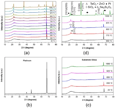
presented inFig. 1a. At room temperature, three peaks corresponding to the 2θangle of 39.68°, 46.12°, and 67.38° were observed. These peaks correspond to platinum (Pt, ICDD reference code: 04-002-0887), which was confirmed by the XRD pattern collected from the plat-inum foil alone, as shown inFig. 1b. The XRD pattern collected from the substrate silica glass is presented inFig. 1c, under the same experimen-tal conditions, which shows a low-intensity band peaked at 25.79° at 1000 °C and a stable peak at 67.38° corresponding to the background platinum foil. This analysis proved the absence of any crystals of detect-able size and the amorphous phase of the base silica up to the maximum temperature employed in this study. Hence, it is asserted that all the peaks (excluding the Pt peaks) appearing in the XRD pattern presented inFig. 1a are those characteristic of EDTS at elevated temperatures.
[image:2.595.93.493.50.424.2]The absence of any significant XRD peak at room temperature vali-dates the amorphous structure of EDTS as fabricated. It is evident from the XRD patterns that the composite material starts to lose its amor-phous nature at temperatures above 600 °C. The diffraction peaks appearing with the increased temperatures from 600 °C onwards indi-cate the progressive crystalline phases in EDTS. However, analysing a mixture of new crystalline phases and a perfect match for all the peaks with the existing ICDD database was not practical. Therefore, the approach here was to identify the known crystal structures and Fig. 1.X-ray diffraction patterns for (a) EDTS as fabricated (25 °C), and in-situ high temperature data between 300 °C and 1000 °C indicating the progressive crystalline phase development of EDTS, (b) platinum foil at room temperature, (c) substrate silica in the temperature range 25 °C to 1000 °C, and (d) selected XRD patterns of EDTS with indexing of the likely peaks corresponding to Na2Si2O5, SiO2, TeO2and ZnO in the temperature range 650 °C to 1000 °C.
compare them to the exact XRD patterns obtained[21].Fig. 1d presents the XRD patterns with indexed peaks corresponding to the possible crystalline structures of Na2Si2O5, SiO2, TeO2and ZnO present in EDTS at high temperatures.
Based on the distinct peaks observed, the XRD patterns could be di-vided into two main regions. Significant crystalline phase developments in the diffraction pattern were observed for 2θangles between 20° and 30° for temperatures above 600 °C, representing the formation and dis-appearance of different crystalline phases, whereas the crystalline phases developed above 600 °C, corresponding to the 2θanglesN30°, show no such remarkable transformations. Notably, both these regions were developed simultaneously after 600 °C as shown inFig. 1a, but the patterns that appeared beyond 2θ= 30° have only steadily growing peaks and no other distinct crystalline phase transformations are de-tected with the temperature rise. In contrast, the patterns observed for 2θangleb30° are not consistent with temperature variations and unveil some interesting crystalline phase formation and disappearance at spe-cific temperature.
The region above 2θ= 30° corresponds to the stable crystalline phases that are formed where the dominant peaks correspond to ZnO and the Pt foil. The peaks at 36.11° and 56.63° match well to that of Zincite (ZnO (101) and (110)), ICDD reference code: 04-008-8199). The intensity of the diffraction peaks increased with temperature, par-ticularly after 800 °C, which could be due to the fact that heat treatment improves the crystal growth of ZnO[22]. The peaks appearing beyond 60° 2θ, except the peak for Pt at 67.38°, were not identified.
The region 2θb30°, random crystalline phase changes are occurring between 600 °C and 900 °C. Two prominent peaks start to appear; at 22.05° and 23.82° that are indexed to Cristobalite (SiO2(101), ICDD ref-erence code: 01-075-0923) and Tellurite (TeO2(111),ICDD reference code: 00-009-0433) respectively at 650 °C. These peaks displayed an in-creasing intensity with temperature indicating the possible increase in
crystallinity in the structure. With the increase in temperature, full-width half maximum (FWHM) of the SiO2peak at 22.05° increased. The appearance of the peak at 23.82° corresponding to TeO2(111) at 650 °C indicates its decomposition from the modified silica network around this temperature. The subsequent vanishing of the TeO223.82° peak at 800 °C was a unique observation that brings in some interesting
findings regarding the crystalline phase dynamics in EDTS. TeO2is vola-tile (heat of vaporization, 52.55 kJ/mol, is the lowest for Te among all other constituents of EDTS) and it was noticed that a considerable amount of tellurium would dissipate during the fabrication process at high temperatures[16,23]. The absence of TeO2peaks at 800 °C shall, therefore, be attributed to a complete evaporation of Te from the EDTS occurring at under hot conditions used in this study. At 850 °C, a new peak at 2θ= 21.09° appeared corresponding to that of sodium silicon oxide (δ-Na2Si2O5(101)/(200)), ICDD reference code:4-009-2739) and remains stable even after cooling the sample. The strongest peak from the reference data for (δ-Na2Si2O5(210)/(111)) (2θ= 22.41°) is weak in the XRD pattern obtained. This could be due to the overlapping by the broader and relatively intense peaks of SiO2. It is interesting to see the formation of Na2Si2O5, which was initiated after the complete release of Te from the EDTS. It might be possible that the absence of Te in the compound facilitated the formation of Na2Si2O5, or it could be purely related to the temperature that supports the growth of Na2Si2O5from the oxides of Na and Si[24]. Remarkably, no peaks corre-sponding to erbium or its associated compound were observed in the analysis. The absence of an erbium compound is likely due to its lower concentrations in EDTS, or possibly, the erbium peaks are enveloped by the presence of other dominant crystalline phases in the EDTS.
The in-situ high-temperature XRDfindings were further validated using the HRTEM and SAED techniques as presented inFig. 2a–h. The HRTEM micrograph inFig. 2a and the clear halo ring pattern in theFig. 2e confirm the absence of any nanocrystallites or other crystalline struc-tures in the EDTS, as fabricated. At 600 °C, the diffracted spots started to appear and it developed with temperature. This is similar to the emer-gence of the 23.82°/22.05° peak observed in the XRD measurements, which was clear at 625 °C. These changes demonstrate the increase in crystallinity of the EDTS with rising temperature. However, not all SAED patterns followed this trend. This could be due to the far smaller volume of the specimen analysed with SAED compared to XRD and thus only collects strong reflections if the crystallites within that small volume exist in the correct orientation with respect to the incoming beam: a fundamental limitation of SAED analysis[21].Fig. 2b, c, d show the micrographs of the sample at high temperatures where the coherently scattering domains are uniformly distributed inside the amorphous matrix indicating the nucleation of nanocrystals. Also, these images clearly show the evolution of crystallites in EDTS with temperature, precisely matching to the XRD observations. The image collected after the cooling of the specimen to room temperature,Fig. 2d and h confirm that the decomposition and the nanocrystallites pro-duced in the EDTS with temperature are irreversible.
All the above results reveal the crystalline phase transitions of a metastable EDTS layer on silica host glass at high temperatures, while a pure silica glass remains in the amorphous phase and does not show these crystalline transformations in the temperature range engaged in this study. Moreover, the study gave a direct observation of the EDTS structural changes from amorphous to crystalline at temperatures above 600 °C. We hypothesize that these crystallisations might be trig-gered by the phase separation of the EDTS and subsequent nucleation of constituents such as ZnO, SiO2, Na2Si2O5and TeO2, which in turn grew subject to the analysis temperature. The distinctive changes in the XRD, SAED pattern, and HRTEM micrographs are a clear validation of nano-crystallite formation in EDTS with increasing temperature.
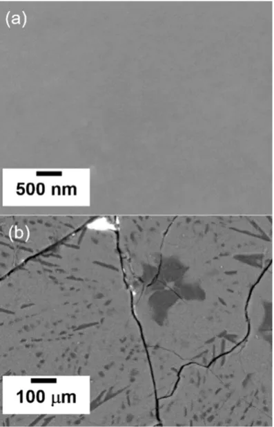
[image:4.595.61.260.53.362.2]The absence of TeO2peaks at 800 °C due to the complete evaporation of Te from the EDTS was later investigated by taking the SEM surface image and SEM-EDX of sample ×1 that underwent the in-situ hot stage XRD. The surface images of the sample before and after the heat Fig. 3.SEM surface image of the sample ×1 (a) as fabricated, (b) after the in-situ hot stage
treatment are displayed inFig. 3a and b respectively, which show that the thermal treatment destroyed the EDTS glassy texture and generated several cracks on the surface. The corresponding SEM-EDX did not show the intensity peaks corresponding to Te in the heat treated sample and confirmed the complete loss of Te from the EDTS at high temperatures. In summary, we have studied the high-temperature effects on the EDTS fabricated by ultrafast laser plasma process and shown that EDTS is thermally stable at temperatures below 600 °C. This leads to the conclusion that EDTS could very well integrate with theSi-photonics manufacturing process, such as a CMOS back-end-of-line process (b500 °C). Additionally, the optical performance of a device fabricated on EDTS will not be affected by the highest rated operating temperature of 85 °C. The dynamics of amorphous to crystalline phase transforma-tion of EDTS with temperature might be more complex than hypothe-sized here. Further studies are proposed to estimate the coordination number of individual ions and morphology of EDTS, which would shed more light on the reaction kinetics associated with the devitrification.
Authors would like to acknowledge the funding from the European Union's Horizon 2020 research and innovation program under the Marie-Skłodowska-Curie grant agreement No 660508. Authors also would like to acknowledge the funding from the Engineering and Physical Sciences Research Council (EPSRC) (EP/M015165/1).
References
[1] W.J. Miniscalco, J. Lightwave Technol. 9 (1991) 234–250.
[2] A. KENYON, Prog. Quantum Electron. 26 (2002) 225–284. [3] G.C. Righini, M. Ferrari, Riv. DEL NUOVO Cim. 28 (2006) 1–53.
[4] M.J.F. Digonnet, Rare Earth Doped Fiber Lasers and Amplifiers, Marcel Dekker, 1993. [5] A. Polman, J. Appl. Phys. 82 (1997) 1.
[6] A. Polman, in: S. Jiang (Ed.), SPIE 3942 2000, pp. 2–13.
[7] S. Serna, W. Zhang, X. Leroux, D. Gao, D. Zhang, L. Vivien, E. Cassan, J. Opt. Soc. Am. B 31 (2014) 2021.
[8] E. Snoeks, P.G. Kik, A. Polman, Opt. Mater. (Amst) 5 (1996) 159–167.
[9] A. Polman, J.S. Custer, P.M. Zagwijn, a.M. Molenbroek, P.F.a. Alkemade, J. Appl. Phys. 81 (1997) 150.
[10] H. Isshiki, F. Jing, T. Sato, T. Nakajima, T. Kimura, Photosynth. Res. 2 (2014) A45. [11] Y. Arakawa, T. Nakamura, Y. Urino, T. Fujita, IEEE Commun. Mag. 51 (2013) 72–77. [12] X. Chen, C. Li, H.K. Tsang, NPG Asia Mater. 3 (2011) 34–40.
[13] M.J.R. Heck, J.F. Bauters, M.L. Davenport, J.K. Doylend, S. Jain, G. Kurczveil, S. Srinivasan, J.E. Bowers, IEEE J. Sel. Top. Quantum Electron. 19 (2013) 6100117. [14] R. Soref, IEEE J. Sel. Top. Quantum Electron. 12 (2006) 1678–1687.
[15] S. Fathpour, Nanophotonics 4 (2015) 143–164.
[16] J. Chandrappan, M. Murray, T. Kakkar, P. Petrik, E. Agocs, Z. Zolnai, D.P. Steenson, A. Jha, G. Jose, Sci. Rep. 5 (2015) 14037.
[17]G. Jose, T.T. Fernandez, D. Steenson, A. Jha, Conf. Lasers Electro-Optics 2012, 2012 (CM3L.6).
[18] J. Chandrappan, M. Murray, P. Petrik, E. Agocs, Z. Zolnai, A. Tempez, S. Legendre, D.P. Steenson, A. Jha, G. Jose, Opt. Mater. Express 5 (2015) 2849.
[19] K.C. Phillips, H.H. Gandhi, E. Mazur, S.K. Sundaram, Adv. Opt. Photon. 7 (2015) 684–712.
[20] L.A. Giannuzzi, F.A. Stevie, Micron 30 (1999) 197–204.
[21] B. Fultz, J. Howe, Transmission Electron Microscopy and Diffractometry of Materials, Springer Berlin Heidelberg, Berlin, Heidelberg, 2013.
[22] K.J. Chen, T.H. Fang, F.Y. Hung, L.W. Ji, S.J. Chang, S.J. Young, Y.J. Hsiao, Appl. Surf. Sci. 254 (2008) 5791–5795.
[23] P. Balling, J. Schou, Rep. Prog. Phys. 76 (2013) 36502.