materials
Article
Thermally Stable Solution Processed Vanadium
Oxide as a Hole Extraction Layer in Organic
Solar Cells
Abdullah Alsulami
1, Jonathan Griffin
1, Rania Alqurashi
1, Hunan Yi
2, Ahmed Iraqi
2,
David Lidzey
1and Alastair Buckley
1,*
1 Department of Physics & Astronomy, University of Sheffield, Hicks Building, Hounsfield Rd., Sheffield,
South Yorkshire S3 7RH, UK; [email protected] (A.A.); [email protected] (J.G.); [email protected] (R.A.); [email protected] (D.L.)
2 Department of Chemistry, University of Sheffield, Sheffield, South Yorkshire S3 7HF, UK;
[email protected] (H.Y.); [email protected] (A.I.)
* Correspondence: [email protected]; Tel.: +44-0114-22-23597
Academic Editor: Lioz Etgar
Received: 16 February 2016; Accepted: 22 March 2016; Published: 25 March 2016
Abstract:
Low-temperature solution-processable vanadium oxide (V
2O
x) thin films have been
employed as hole extraction layers (HELs) in polymer bulk heterojunction solar cells. V
2O
xfilms
were fabricated in air by spin-coating vanadium(V) oxytriisopropoxide (s-V
2O
x) at room temperature
without the need for further thermal annealing. The deposited vanadium(V) oxytriisopropoxide film
undergoes hydrolysis in air, converting to V
2O
xwith optical and electronic properties comparable to
vacuum-deposited V
2O
5. When s-V
2O
xthin films were annealed in air at temperatures of 100
˝C and
200
˝C, OPV devices showed similar results with good thermal stability and better light transparency.
Annealing at 300
˝C and 400
˝C resulted in a power conversion efficiency (PCE) of 5% with a
decrement approximately 15% lower than that of unannealed films; this is due to the relative decrease
in the shunt resistance (R
sh) and an increase in the series resistance (R
s) related to changes in the
oxidation state of vanadium.
Keywords:
organic photovoltaic; vanadium oxide; thermal stability; solution processing;
photoelectron spectroscopy
1. Introduction
Currently, the high cost of commercial inorganic photovoltaics remains an obstacle for the
wide-scale installation in both residential and commercial settings [
1
]. In order to overcome this
high cost, researchers have studied numerous materials as alternatives, with organic polymer
solar cells being a promising candidate [
2
,
3
]. This is due to organic polymers exhibiting several
advantageous properties, such as solution-processability, mechanical-flexibility, and thin device
architectures allowing for light-weight devices [
4
–
6
]. This combination of factors allows organic
solar to scale up manufacture via roll-to-roll- or sheet-to-sheet-based deposition techniques leading
to reduced fabrication costs. Recent advances in polymer synthesis and device processing have
pushed the power conversion efficiency of single junction cells as high as 10.8% [
7
]. These efficiencies
are above the 10% mark often quoted as the point at which polymer photovoltaics will become
commercially viable.
However, currently, the lifetime of devices incorporating the highest
performing materials are below the 10 year mark required; one method to improve the lifetime
of devices is to replace the commonly-used hole extraction interfacial layer (HELs), polyethylene
dioxythiophene:polystyrenesulfonate (PEDOT:PSS) [
8
–
10
]. This is because, despite the positive aspects
of aqueous PEDOT:PSS, the residual moisture and the acidic nature of PEDOT:PSS can cause
degradation of the electrode and organic films and, therefore, reduce the devices operational
lifetime [
11
–
14
]. To overcome some of these issues thin metal oxides such as MoO
3, WO
3, NiO,
and V
2O
5have been used; these materials have been shown to exhibit performances that are similar
to or better than OPVs with an interfacial PEDOT:PSS layer [
15
–
18
]. Not only are these materials of
interest in organic photovoltaics because of their unique electronic properties and chemical stability,
they are also being used in other photovoltaic technologies such as CiGS, and CdTe [
19
–
22
]. However,
like PEDOT:PSS the presence of water can lead to changes at the interface between metal oxides
and organic semiconductors, due to the intercalation of water within metal oxide clusters leading to
changes within the energy level structure [
23
]. This makes the improvement of processing conditions
and reduction in the cost and complexity of depositing these interfacial layers highly desirable.
Solution-processing of the metal oxide interfacial layers has shown significant promise for
reducing the complexity of the deposition of these materials. Previous studies have shown that
vanadium oxide can be deposited from solution at low temperature in air without the need for any high
temperature post-deposition treatments [
24
–
28
]. On the other hand, some optoelectronic devices which
are fabricated at high temperatures require developed metal oxides which must be able to keep their
properties under high temperature fabrication processes. Whilst the optical and chemical properties of
V
2O
xhave previously been investigated after high-temperature annealing [
29
–
31
], its performance
with OPVs has not. Therefore, our motivation for this work is to explore the impact of thermal heating
on V
2O
xthin films as HELs in organic solar cells.
In this paper we incorporated V
2O
xthin films deposited from a vanadium(V) oxytriisopropoxide
precursor into PFDT2BT-8:PC
70BM OPV devices achieving a power conversion efficiency of 6%,
comparable to PEDOT:PSS and vacuum deposited MoO
3. Furthermore, we fabricated some OPV
devices with annealed V
2O
xlayers at high temperatures in air before spin coating the active
layer to study their thermal stability. We demonstrated that OPV devices show PCE
ě
5% with
thermally-annealed V
2O
xat 400
˝C. Absorption spectroscopy, X-ray photoelectron spectroscopy (XPS),
and ultraviolet photoelectron spectroscopy (UPS) are combined to explain the J–V characteristics
of OPVs.
2. Results and Discussion
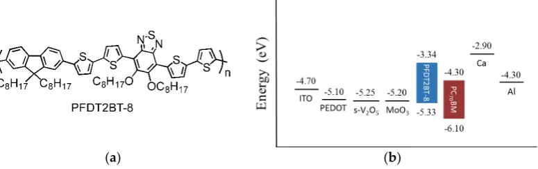
2.1. PFDT2BT-8 Structure
The chemical structure of our donor polymer used in this work is shown in Figure
1
a [
32
].
The highest occupied molecular orbital (HOMO) energy level and lowest unoccupied molecular
orbital (LUMO) of PFDT2BT-8 are
´
5.33 eV and
´
3.34 eV, respectively, as determined from a cyclic
voltammetry. The energy band diagram and work function of the relative materials in our study are
presented in Figure
1
b [
32
,
33
].
Materials 2016, 9, 235 2 of 11
[image:2.595.106.494.591.713.2]degradation
of
the
electrode
and
organic
films
and,
therefore,
reduce
the
devices
operational
lifetime
[11–14].
To
overcome
some
of
these
issues
thin
metal
oxides
such
as
MoO
3,
WO
3,
NiO,
and
V
2O
5have
been
used;
these
materials
have
been
shown
to
exhibit
performances
that
are
similar
to
or
better
than
OPVs
with
an
interfacial
PEDOT:PSS
layer
[15–18].
Not
only
are
these
materials
of
interest
in
organic
photovoltaics
because
of
their
unique
electronic
properties
and
chemical
stability,
they
are
also
being
used
in
other
photovoltaic
technologies
such
as
CiGS,
and
CdTe
[19–22].
However,
like
PEDOT:PSS
the
presence
of
water
can
lead
to
changes
at
the
interface
between
metal
oxides
and
organic
semiconductors,
due
to
the
intercalation
of
water
within
metal
oxide
clusters
leading
to
changes
within
the
energy
level
structure
[23].
This
makes
the
improvement
of
processing
conditions
and
reduction
in
the
cost
and
complexity
of
depositing
these
interfacial
layers
highly
desirable.
Solution
‐
processing
of
the
metal
oxide
interfacial
layers
has
shown
significant
promise
for
reducing
the
complexity
of
the
deposition
of
these
materials.
Previous
studies
have
shown
that
vanadium
oxide
can
be
deposited
from
solution
at
low
temperature
in
air
without
the
need
for
any
high
temperature
post
‐
deposition
treatments
[24–28].
On
the
other
hand,
some
optoelectronic
devices
which
are
fabricated
at
high
temperatures
require
developed
metal
oxides
which
must
be
able
to
keep
their
properties
under
high
temperature
fabrication
processes.
Whilst
the
optical
and
chemical
properties
of
V2O
xhave
previously
been
investigated
after
high
‐
temperature
annealing
[29–31],
its
performance
with
OPVs
has
not.
Therefore,
our
motivation
for
this
work
is
to
explore
the
impact
of
thermal
heating
on
V
2O
xthin
films
as
HELs
in
organic
solar
cells.
In
this
paper
we
incorporated
V
2O
xthin
films
deposited
from
a
vanadium(V)
oxytriisopropoxide
precursor
into
PFDT2BT
‐
8:PC70BM
OPV
devices
achieving
a
power
conversion
efficiency
of
6%,
comparable
to
PEDOT:PSS
and
vacuum
deposited
MoO3.
Furthermore,
we
fabricated
some
OPV
devices
with
annealed
V
2O
xlayers
at
high
temperatures
in
air
before
spin
coating
the
active
layer
to
study
their
thermal
stability.
We
demonstrated
that
OPV
devices
show
PCE
≥
5%
with
thermally
‐
annealed
V2O
xat
400
°C.
Absorption
spectroscopy,
X
‐
ray
photoelectron
spectroscopy
(XPS),
and
ultraviolet
photoelectron
spectroscopy
(UPS)
are
combined
to
explain
the
J–
V
characteristics
of
OPVs.
2.
Results
and
Discussion
2.1.
PFDT2BT
‐
8
Structure
The
chemical
structure
of
our
donor
polymer
used
in
this
work
is
shown
in
Figure
1a
[32].
The
highest
occupied
molecular
orbital
(HOMO)
energy
level
and
lowest
unoccupied
molecular
orbital
(LUMO)
of
PFDT2BT
‐
8
are
−
5.33
eV
and
−
3.34
eV,
respectively,
as
determined
from
a
cyclic
voltammetry.
The
energy
band
diagram
and
work
function
of
the
relative
materials
in
our
study
are
presented
in
Figure
1b
[32,33].
(
a
)
(
b
)
Figure 1. (a) The chemical structure of PFDT2BT‐8; and (b) energy levels of electrodes, HELs, and
active layer materials used in this work.
2.2.
s
‐
V
2O
xas
a
Hole
Extraction
Layer
To
assess
the
performance
of
PFDT2BT
‐
8
polymer
with
the
s
‐
V2O
xinterlayer,
we
fabricated
sets
of
PFDT2BT
‐
8:PC70BM
devices
with
variable
thicknesses
of
s
‐
V2O
x.
The
extracted
data
suggests
an
Materials2016,9, 235 3 of 12
2.2. s-V
2O
xas a Hole Extraction Layer
To assess the performance of PFDT2BT-8 polymer with the s-V
2O
xinterlayer, we fabricated sets
of PFDT2BT-8:PC
70BM devices with variable thicknesses of s-V
2O
x. The extracted data suggests an
optimum s-V
2O
xlayer thickness below 10 nm. Therefore, we selected a layer thickness of 5 nm for all
s-V
2O
xdevices.
Figure
2
shows the J–V characteristics of our OPV devices and those of the most widely used
HELs, PEDOT:PSS and thermally evaporated MoO
3under AM 1.5 G illumination. It can be seen that
using PEDOT:PSS and s-V
2O
xlayers as HEL showed a similar photovoltaic response (PCE = 6.5%)
which is better than devices fabricated with MoO
3interlayer (PCE = 6.3%). These results indicate that
a high performance can be achieved for PFDT2BT-8 devices by using untreated s-V
2O
xfilms which are
in good agreement with the previous studies in literature [
25
,
27
,
34
].
Materials 2016, 9, 235 3 of 11
optimum s‐V2Ox layer thickness below 10 nm. Therefore, we selected a layer thickness of 5 nm for all
s‐V2Ox devices.
Figure 2 shows the J–V characteristics of our OPV devices and those of the most widely used
HELs, PEDOT:PSS and thermally evaporated MoO3 under AM 1.5 G illumination.
It can be seen that
using PEDOT:PSS and s‐V2Ox layers as HEL showed a similar photovoltaic response (PCE = 6.5%)
which is better than devices fabricated with MoO3 interlayer (PCE = 6.3%). These results indicate that
a high performance can be achieved for PFDT2BT‐8 devices by using untreated s‐V2Ox films which
are in good agreement with the previous studies in literature [25,27,34].
Figure 2. The current density‐voltage characteristics of PFDT2BT‐8:PC70BM based solar cell with (□)
PEDOT:PSS, ( ) s‐V2Ox, and ( ) MoO3.
To explore the effect of thermal annealing (≥100 °C) on the photovoltaic response of our devices,
s‐V2Ox films were annealed in air at temperatures of 100, 200, 300, and 400 °C for 30 min before spin
coating the active layer. The corresponding current‐voltage characteristic of OPVs is shown in
Figure 3. The photovoltaic parameters obtained are summarised in Table 1 which represent the
average of at least 12 pixels from 18 pixels defined on three separate substrates. The errors quoted
are defined by the standard deviation about the mean.
Figure 3. The current density‐voltage characteristics of organic solar cell with (□) unannealed s‐V2Ox
interlayer and annealed at ( ) 100 °C, ( ) 200 °C, ( ) 300 °C, and ( ) 400 °C for 30 min.
0.0 0.2 0.4 0.6 0.8 1.0
-10
-8
-6
-4
-2
0
2
C
ur
renst
densi
ty
(m
A/
cm
2)
Voltage (V)
0.0
0.2
0.4
0.6
0.8
1.0
-10
-8
-6
-4
-2
0
2
Current
de
nsi
ty
(mA/c
m
2)
Voltage (V)
Figure 2.The current density-voltage characteristics of PFDT2BT-8:PC70BM based solar cell with (2) PEDOT:PSS, (
Materials 2016, 9, 235 4 of 11
Table 1. Summary of solar cell parameters with s‐V2Ox buffer layer annealed at different temperatures for different periods of time.
Ann. Temp.
Maximum PCE (%)
Average PCE(av) (%)
Voc (V)
Jsc
(mA∙cm−2)
FF (%)
Rs
(Ω∙cm2)
Rsh
(Ω∙cm2)
Non 6.0 5.8 ± 0.14 0.86 10.0 ± 0.22 67.1 ± 1.2 11.6 ± 0.9 1264 ± 91
100 6.0 5.9 ± 0.14 0.86 10.1 ± 0.13 68.3 ± 1.7 10.5 ± 1.0 1282 ± 215
200 6.3 5.9 ± 0.26 0.87 10.2 ± 0.14 67.1 ± 2.6 10.3 ± 0.7 1346 ± 246
300 5.6 5.3 ± 0.28 0.83 9.9 ± 0.41 64.3 ± 2.7 12.6 ± 1.7 1095 ± 238
400 5.2 5.0 ± 0.17 0.83 10.1 ± 0.12 59.6 ± 0.9 17.6 ± 0.4 933 ± 84
It can be seen that the performance of devices annealed at temperatures 100 or 200 °C is quite
similar to those prepared without heat treatment. The slight increase in PCE of devices annealed up
to 200 °C can be ascribed to the relative increase in the shunt resistance Rsh and decrease in the series
resistance Rs. In contrast, as the film annealing temperature is raised to 400 °C, OPV devices show a
PCE of 5% with a decrement approximately 15% lower than that of those with unannealed films. It is
clear from Table 1 that the relatively weak photovoltaic response can be attributed to the decrease in
open‐circuit voltage, due to the change in chemical structure as will be discussed based on the XPS
data later on. Furthermore, the shunt resistance falls considerably on annealing above 300 °C
reaching a minimum Rsh of 933 Ω∙cm2 on annealing at 400 °C due to the recombination process at the
anode interface. This caused a decrease in hole density at the anode interface leading to a decrease in
the internal electric field [35,36].
2.3. Optical Properties
To understand the changes that we observed in the photovoltaic response as a function of the
annealing temperature, we investigated the optical properties of annealed s‐V2Ox films. Figure 4
presents the optical transmittance of the films as a function of the wavelength for the as‐deposited
and annealed films. All s‐V2Ox films show high transmission for wavelengths above 500 nm covering
the majority of the solar spectrum. The transmittance in the visible wavelength range, from 400 to
500 nm, increases slightly by annealing up to 300 °C which is attributed to change of the films
refractive index related to chemical structure changes. On annealing to 400 °C, the film exhibits
absorption peak at 415 nm which could be ascribed to small polaron absorption [37,38]. This effect
results from disordering defects in V2Ox structure leading to transferring charges between
neighbouring sites with a significant spread in energy.
Figure 4. Optical transmission spectra of the s‐V2Ox films with different Annealing temperature; (□) unannealed, ( ) 100 °C, ( ) 200 °C, ( ) 300 °C, and ( ) 400 °C. The insert shows the absorption
coefficient (αhν)2 as a function of the photon energy.
400 500 600 700 800
0.4 0.5 0.6 0.7 0.8 0.9 1.0 Tra nsmittan ce Wavelength (nm)
2.2 2.4 2.6 2.8 3.0 3.2 0.00 0.02 0.04 h
x 10 10 (eV
/cm
)
2
E (eV)
) s-V2Ox, and (
Materials 2016, 9, 235 7 of 11
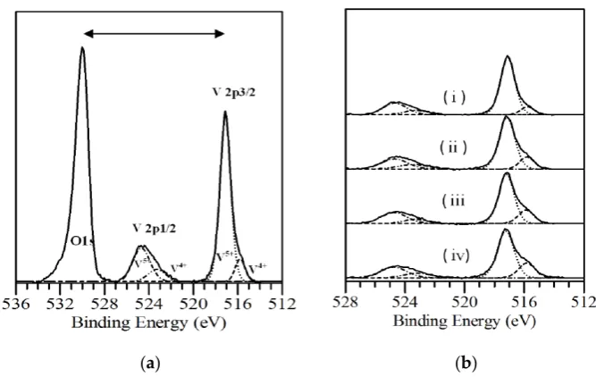
Table 2. Summary of solar cell parameters with s‐V2Ox buffer layer annealed at different temperatures for different periods of time.
Annealing Temperature
V4+ Oxidation State
V5+Oxidation
State
Work Function (eV)
Valence
Band (eV) (eV)
Unannealing 15% 85% 5.26 2.53 2.5
200 °C 22.5% 77.5% 5.22 2.53 3.78
300 °C 27% 73% 5.23 2.50 2.68
400 °C 33% 67% 5.19 2.50 2.42
2.6. Ultraviolet Photoelectron Spectroscopy
Figure 7 plots the UPS spectra of V2Ox films that have been annealed at different temperatures.
The work function and valence band edge determined by the UPS are also summarised in Table 1.
As shown in Figure 7a, the position of the secondary electron cut‐off for unannealed film was
determined to be at the binding energy of 15.94 eV below the Fermi level, corresponding to a work
function of 5.26 eV. Compared to previous studies, the work function of our s‐V2Ox films is similar to
those prepared by different processes [34]. On annealing, the secondary electron cut‐off shows a
slight shift up to 0.07 eV toward the higher binding energy. While we see a 0.07 eV change in the
work function we can’t assign these changes directly to the processing of the s‐V2Ox due to the
possible influence of adsorbates. Figure 7b displays the onset of the s‐V2Ox valence band to be 2.5 eV
below the Fermi level which is identical with all samples.
We did not notice any shift for the valence
band maximum with increase annealing temperature. Careful observation of the valence band
region of films annealed at 300 °C and 400 °C reveals the formation of more gap states at 1 eV below
the Fermi level as shown in the inset of Figure 7b. This suggests that oxygen vacancies shift the
Fermi level up toward the conduction band leaving some occupied states within the band gap.
Therefore, introducing oxygen vacancies can act as n‐type dopants resulting in a decrease in the
work function of vanadium oxide [53]. Consequently, photoelectron spectroscopy analysis confirms
that the high‐temperature annealing of s‐V2Ox film produces a change in the chemical structure of
the vanadium oxide layer and, thus, increases slightly the hole‐electron recombination at the
interface. Nevertheless, our experiments demonstrate that s‐V2Ox film can be used to replace
evaporated metal oxides in optoelectronic devices which are fabricated at high temperatures.
6 5 4 3 2 1 0
Intensity (counts)
Binding energy eV
2.5 2.0 1.5 1.0 0.5 0.0
(a)
(b)
Figure 7. UPS measurements for V2Ox films Span coated on ITO in ambient conditions with no annealing and annealed, (□) unannealed, ( ) 200 °C, ( ) 300 °C, and ( ) 400 °C. (a) shows the
secondary electron cut‐off region; and (b) shows the expanded region near the Fermi level; the insert
shows the density of gap states formed about 1 eV below the Fermi level.
16.2 16.1 16.0 15.9 15.8
In
ten
sity (
co
unts)
Binding Energy eV
) MoO3.
To explore the effect of thermal annealing (
ě
100
˝C) on the photovoltaic response of our devices,
s-V
2O
xfilms were annealed in air at temperatures of 100, 200, 300, and 400
˝C for 30 min before spin
coating the active layer. The corresponding current-voltage characteristic of OPVs is shown in Figure
3
.
The photovoltaic parameters obtained are summarised in Table
1
which represent the average of at
least 12 pixels from 18 pixels defined on three separate substrates. The errors quoted are defined by
the standard deviation about the mean.
Materials 2016, 9, 235 3 of 11
optimum s‐V2Ox layer thickness below 10 nm. Therefore, we selected a layer thickness of 5 nm for all
s‐V2Ox devices.
Figure 2 shows the J–V characteristics of our OPV devices and those of the most widely used
HELs, PEDOT:PSS and thermally evaporated MoO3 under AM 1.5 G illumination.
It can be seen that
using PEDOT:PSS and s‐V2Ox layers as HEL showed a similar photovoltaic response (PCE = 6.5%)
which is better than devices fabricated with MoO3 interlayer (PCE = 6.3%). These results indicate that
a high performance can be achieved for PFDT2BT‐8 devices by using untreated s‐V2Ox films which
are in good agreement with the previous studies in literature [25,27,34].
Figure 2. The current density‐voltage characteristics of PFDT2BT‐8:PC70BM based solar cell with (□)
PEDOT:PSS, ( ) s‐V2Ox, and ( ) MoO3.
To explore the effect of thermal annealing (≥100 °C) on the photovoltaic response of our devices,
s‐V2Ox films were annealed in air at temperatures of 100, 200, 300, and 400 °C for 30 min before spin
coating the active layer. The corresponding current‐voltage characteristic of OPVs is shown in
Figure 3. The photovoltaic parameters obtained are summarised in Table 1 which represent the
average of at least 12 pixels from 18 pixels defined on three separate substrates. The errors quoted
are defined by the standard deviation about the mean.
Figure 3. The current density‐voltage characteristics of organic solar cell with (□) unannealed s‐V2Ox
interlayer and annealed at ( ) 100 °C, ( ) 200 °C, ( ) 300 °C, and ( ) 400 °C for 30 min.
0.0 0.2 0.4 0.6 0.8 1.0
-10
-8
-6
-4
-2
0
2
C
ur
renst
densi
ty
(m
A/
cm
2)
Voltage (V)
0.0
0.2
0.4
0.6
0.8
1.0
-10
-8
-6
-4
-2
0
2
Current
de
nsi
ty
(mA/c
m
2)
Voltage (V)
Figure 3.The current density-voltage characteristics of organic solar cell with (2) unannealed s-V2Ox
interlayer and annealed at (
Materials 2016, 9, 235 4 of 11
Table 1. Summary of solar cell parameters with s‐V2Ox buffer layer annealed at different temperatures for different periods of time.
Ann. Temp.
Maximum PCE (%)
Average PCE(av) (%)
Voc (V)
Jsc
(mA∙cm−2)
FF (%)
Rs
(Ω∙cm2)
Rsh
(Ω∙cm2)
Non 6.0 5.8 ± 0.14 0.86 10.0 ± 0.22 67.1 ± 1.2 11.6 ± 0.9 1264 ± 91
100 6.0 5.9 ± 0.14 0.86 10.1 ± 0.13 68.3 ± 1.7 10.5 ± 1.0 1282 ± 215
200 6.3 5.9 ± 0.26 0.87 10.2 ± 0.14 67.1 ± 2.6 10.3 ± 0.7 1346 ± 246
300 5.6 5.3 ± 0.28 0.83 9.9 ± 0.41 64.3 ± 2.7 12.6 ± 1.7 1095 ± 238
400 5.2 5.0 ± 0.17 0.83 10.1 ± 0.12 59.6 ± 0.9 17.6 ± 0.4 933 ± 84
It can be seen that the performance of devices annealed at temperatures 100 or 200 °C is quite
similar to those prepared without heat treatment. The slight increase in PCE of devices annealed up
to 200 °C can be ascribed to the relative increase in the shunt resistance Rsh and decrease in the series
resistance Rs. In contrast, as the film annealing temperature is raised to 400 °C, OPV devices show a
PCE of 5% with a decrement approximately 15% lower than that of those with unannealed films. It is
clear from Table 1 that the relatively weak photovoltaic response can be attributed to the decrease in
open‐circuit voltage, due to the change in chemical structure as will be discussed based on the XPS
data later on. Furthermore, the shunt resistance falls considerably on annealing above 300 °C
reaching a minimum Rsh of 933 Ω∙cm2 on annealing at 400 °C due to the recombination process at the
anode interface. This caused a decrease in hole density at the anode interface leading to a decrease in
the internal electric field [35,36].
2.3. Optical Properties
To understand the changes that we observed in the photovoltaic response as a function of the
annealing temperature, we investigated the optical properties of annealed s‐V2Ox films. Figure 4
presents the optical transmittance of the films as a function of the wavelength for the as‐deposited
and annealed films. All s‐V2Ox films show high transmission for wavelengths above 500 nm covering
the majority of the solar spectrum. The transmittance in the visible wavelength range, from 400 to
500 nm, increases slightly by annealing up to 300 °C which is attributed to change of the films
refractive index related to chemical structure changes. On annealing to 400 °C, the film exhibits
absorption peak at 415 nm which could be ascribed to small polaron absorption [37,38]. This effect
results from disordering defects in V2Ox structure leading to transferring charges between
neighbouring sites with a significant spread in energy.
Figure 4. Optical transmission spectra of the s‐V2Ox films with different Annealing temperature; (□) unannealed, ( ) 100 °C, ( ) 200 °C, ( ) 300 °C, and ( ) 400 °C. The insert shows the absorption
coefficient (αhν)2 as a function of the photon energy.
400 500 600 700 800
0.4 0.5 0.6 0.7 0.8 0.9 1.0 Tra nsmittan ce Wavelength (nm)
2.2 2.4 2.6 2.8 3.0 3.2 0.00 0.02 0.04 h
x 10 10 (eV
/cm
)
2
E (eV)
) 100˝C, (
Materials 2016, 9, 235 7 of 11
Table 2. Summary of solar cell parameters with s‐V2Ox buffer layer annealed at different temperatures for different periods of time.
Annealing Temperature
V4+ Oxidation State
V5+Oxidation
State
Work Function (eV)
Valence
Band (eV) (eV)
Unannealing 15% 85% 5.26 2.53 2.5
200 °C 22.5% 77.5% 5.22 2.53 3.78
300 °C 27% 73% 5.23 2.50 2.68
400 °C 33% 67% 5.19 2.50 2.42
2.6. Ultraviolet Photoelectron Spectroscopy
Figure 7 plots the UPS spectra of V2Ox films that have been annealed at different temperatures.
The work function and valence band edge determined by the UPS are also summarised in Table 1.
As shown in Figure 7a, the position of the secondary electron cut‐off for unannealed film was
determined to be at the binding energy of 15.94 eV below the Fermi level, corresponding to a work
function of 5.26 eV. Compared to previous studies, the work function of our s‐V2Ox films is similar to
those prepared by different processes [34]. On annealing, the secondary electron cut‐off shows a
slight shift up to 0.07 eV toward the higher binding energy. While we see a 0.07 eV change in the
work function we can’t assign these changes directly to the processing of the s‐V2Ox due to the
possible influence of adsorbates. Figure 7b displays the onset of the s‐V2Ox valence band to be 2.5 eV
below the Fermi level which is identical with all samples.
We did not notice any shift for the valence
band maximum with increase annealing temperature. Careful observation of the valence band
region of films annealed at 300 °C and 400 °C reveals the formation of more gap states at 1 eV below
the Fermi level as shown in the inset of Figure 7b. This suggests that oxygen vacancies shift the
Fermi level up toward the conduction band leaving some occupied states within the band gap.
Therefore, introducing oxygen vacancies can act as n‐type dopants resulting in a decrease in the
work function of vanadium oxide [53]. Consequently, photoelectron spectroscopy analysis confirms
that the high‐temperature annealing of s‐V2Ox film produces a change in the chemical structure of
the vanadium oxide layer and, thus, increases slightly the hole‐electron recombination at the
interface. Nevertheless, our experiments demonstrate that s‐V2Ox film can be used to replace
evaporated metal oxides in optoelectronic devices which are fabricated at high temperatures.
6 5 4 3 2 1 0
Intensity (counts)
Binding energy eV
2.5 2.0 1.5 1.0 0.5 0.0
(a)
(b)
Figure 7. UPS measurements for V2Ox films Span coated on ITO in ambient conditions with no annealing and annealed, (□) unannealed, ( ) 200 °C, ( ) 300 °C, and ( ) 400 °C. (a) shows the
secondary electron cut‐off region; and (b) shows the expanded region near the Fermi level; the insert
shows the density of gap states formed about 1 eV below the Fermi level.
16.2 16.1 16.0 15.9 15.8
In
ten
sity (
co
unts)
Binding Energy eV
) 200˝C, (
Materials 2016, 9, 235 7 of 11
Table 2. Summary of solar cell parameters with s‐V2Ox buffer layer annealed at different temperatures for different periods of time.
Annealing Temperature
V4+ Oxidation State
V5+Oxidation
State
Work Function (eV)
Valence
Band (eV) (eV)
Unannealing 15% 85% 5.26 2.53 2.5
200 °C 22.5% 77.5% 5.22 2.53 3.78
300 °C 27% 73% 5.23 2.50 2.68
400 °C 33% 67% 5.19 2.50 2.42
2.6. Ultraviolet Photoelectron Spectroscopy
Figure 7 plots the UPS spectra of V2Ox films that have been annealed at different temperatures.
The work function and valence band edge determined by the UPS are also summarised in Table 1.
As shown in Figure 7a, the position of the secondary electron cut‐off for unannealed film was
determined to be at the binding energy of 15.94 eV below the Fermi level, corresponding to a work
function of 5.26 eV. Compared to previous studies, the work function of our s‐V2Ox films is similar to
those prepared by different processes [34]. On annealing, the secondary electron cut‐off shows a
slight shift up to 0.07 eV toward the higher binding energy. While we see a 0.07 eV change in the
work function we can’t assign these changes directly to the processing of the s‐V2Ox due to the
possible influence of adsorbates. Figure 7b displays the onset of the s‐V2Ox valence band to be 2.5 eV
below the Fermi level which is identical with all samples.
We did not notice any shift for the valence
band maximum with increase annealing temperature. Careful observation of the valence band
region of films annealed at 300 °C and 400 °C reveals the formation of more gap states at 1 eV below
the Fermi level as shown in the inset of Figure 7b. This suggests that oxygen vacancies shift the
Fermi level up toward the conduction band leaving some occupied states within the band gap.
Therefore, introducing oxygen vacancies can act as n‐type dopants resulting in a decrease in the
work function of vanadium oxide [53]. Consequently, photoelectron spectroscopy analysis confirms
that the high‐temperature annealing of s‐V2Ox film produces a change in the chemical structure of
the vanadium oxide layer and, thus, increases slightly the hole‐electron recombination at the
interface. Nevertheless, our experiments demonstrate that s‐V2Ox film can be used to replace
evaporated metal oxides in optoelectronic devices which are fabricated at high temperatures.
6 5 4 3 2 1 0
Intensity (counts)
Binding energy eV
2.5 2.0 1.5 1.0 0.5 0.0
(a)
(b)
Figure 7. UPS measurements for V2Ox films Span coated on ITO in ambient conditions with no annealing and annealed, (□) unannealed, ( ) 200 °C, ( ) 300 °C, and ( ) 400 °C. (a) shows the
secondary electron cut‐off region; and (b) shows the expanded region near the Fermi level; the insert
shows the density of gap states formed about 1 eV below the Fermi level.
16.2 16.1 16.0 15.9 15.8
In
ten
sity (
co
unts)
Binding Energy eV
) 300˝C, and (
Materials 2016, 9, 235 4 of 11
Table 1. Summary of solar cell parameters with s‐V2Ox buffer layer annealed at different temperatures for different periods of time.
Ann. Temp.
Maximum PCE (%)
Average PCE(av) (%)
Voc (V)
Jsc
(mA∙cm−2)
FF (%)
Rs
(Ω∙cm2)
Rsh
(Ω∙cm2)
Non 6.0 5.8 ± 0.14 0.86 10.0 ± 0.22 67.1 ± 1.2 11.6 ± 0.9 1264 ± 91
100 6.0 5.9 ± 0.14 0.86 10.1 ± 0.13 68.3 ± 1.7 10.5 ± 1.0 1282 ± 215
200 6.3 5.9 ± 0.26 0.87 10.2 ± 0.14 67.1 ± 2.6 10.3 ± 0.7 1346 ± 246
300 5.6 5.3 ± 0.28 0.83 9.9 ± 0.41 64.3 ± 2.7 12.6 ± 1.7 1095 ± 238
400 5.2 5.0 ± 0.17 0.83 10.1 ± 0.12 59.6 ± 0.9 17.6 ± 0.4 933 ± 84
It can be seen that the performance of devices annealed at temperatures 100 or 200 °C is quite
similar to those prepared without heat treatment. The slight increase in PCE of devices annealed up
to 200 °C can be ascribed to the relative increase in the shunt resistance Rsh and decrease in the series
resistance Rs. In contrast, as the film annealing temperature is raised to 400 °C, OPV devices show a
PCE of 5% with a decrement approximately 15% lower than that of those with unannealed films. It is
clear from Table 1 that the relatively weak photovoltaic response can be attributed to the decrease in
open‐circuit voltage, due to the change in chemical structure as will be discussed based on the XPS
data later on. Furthermore, the shunt resistance falls considerably on annealing above 300 °C
reaching a minimum Rsh of 933 Ω∙cm2 on annealing at 400 °C due to the recombination process at the
anode interface. This caused a decrease in hole density at the anode interface leading to a decrease in
the internal electric field [35,36].
2.3. Optical Properties
To understand the changes that we observed in the photovoltaic response as a function of the
annealing temperature, we investigated the optical properties of annealed s‐V2Ox films. Figure 4
presents the optical transmittance of the films as a function of the wavelength for the as‐deposited
and annealed films. All s‐V2Ox films show high transmission for wavelengths above 500 nm covering
the majority of the solar spectrum. The transmittance in the visible wavelength range, from 400 to
500 nm, increases slightly by annealing up to 300 °C which is attributed to change of the films
refractive index related to chemical structure changes. On annealing to 400 °C, the film exhibits
absorption peak at 415 nm which could be ascribed to small polaron absorption [37,38]. This effect
results from disordering defects in V2Ox structure leading to transferring charges between
neighbouring sites with a significant spread in energy.
Figure 4. Optical transmission spectra of the s‐V2Ox films with different Annealing temperature; (□) unannealed, ( ) 100 °C, ( ) 200 °C, ( ) 300 °C, and ( ) 400 °C. The insert shows the absorption
coefficient (αhν)2 as a function of the photon energy.
400 500 600 700 800
0.4 0.5 0.6 0.7 0.8 0.9 1.0 Tra nsmittan ce Wavelength (nm)
2.2 2.4 2.6 2.8 3.0 3.2 0.00 0.02 0.04 h
x 10 10 (eV
/cm
)
2
E (eV)
[image:3.595.188.406.254.417.2]